 | –≠–ª–µ–∫—Ç—Ä–æ–Ω–Ω—ã–π –∫–æ–º–ø–æ–Ω–µ–Ω—Ç: HA12231 | –°–∫–∞—á–∞—Ç—å:  PDF PDF  ZIP ZIP |

HA12231FP
Audio Signal Processor for Car Deck (PB 1 Chip)
ADE-207-327A (Z)
2nd Edition
Jan. 2001
Description
HA12231FP is silicon monolithic bipolar IC providing PB equalizer system and music sensor system in
one chip.
Functions
∑
PB equalizer
◊
2 channel
∑
Music sensor
◊
1 channel
∑
Line amp.
◊
2 channel
∑
Line mute
◊
2 channel
Features
∑
No use external parts for PB equalizer. (Fixed characteristics built-in)
∑
Available to change music sensing level by external resistor.
∑
Available to change frequency response of music sensor by external capacitor.
∑
Different type of PB equalizer characteristics selection (120
µ
s/70
µ
s) is available.
∑
Line mute ON/OFF is avalable.
∑
This IC is strong for a cellular phone noise.
Ordering Information
Functions
Product
Package
PBOUT-Level
PB-EQ
Music Sensor
Mute
HA12231FP
FP-20DA
450 mVrms
r
r
r

HA12231FP
2
Pin Description, Equivalent Circuit (V
CC
= 9 V, A system of single supply voltage,
Ta = 25
∞
C, No Signal, The value in the table shows typical value.)
Pin No.
Pin Name
Note
Equivalent Circuit
Description
16
TAI(L)
V = V
CC
/2
V
CC
/2
V
100 k
Tape input
5
TAI(R)
14
RIP
V = V
CC
/2
GND
V
CC
V
Ripple filter
13
MS DET
V = V
CC
GND
Time constant pin for rectifier
15
PBOUT(L)
V = V
CC
/2
V
CC
GND
V
PB output
6
PBOUT(R)
1
VREF
V = V
CC
/2
V
CC
GND
V
Reference output
17
EQOUT(L)
V = V
CC
/2
Equalizer output (120
µ
)
4
EQOUT(R)
Note:
MS: Music Sensor

HA12231FP
3
Pin Description, Equivalent Circuit (V
CC
= 9 V, A system of single supply voltage,
Ta = 25
∞
C, No Signal, The value in the table shows typical value.) (cont.)
Pin No.
Pin Name
Note
Equivalent Circuit
Description
11
V
CC
Power supply
19
FIN(L)
V
Equalizer input
18
RIN(L)
3
RIN(R)
2
FIN(R)
9
Mute
22 k
GND
100 k
Mode control input
10
FOR
/REV
8
120
/70
12
MS
I
100 k
200
MS V
CC
D GND
MS output (to MPU) *
7
MS G
V
V = V
CC
/2
V
90 k
MS gain pin *
20
GND
GND pin
Note:
MS: Music Sensor
HA12231FP
4
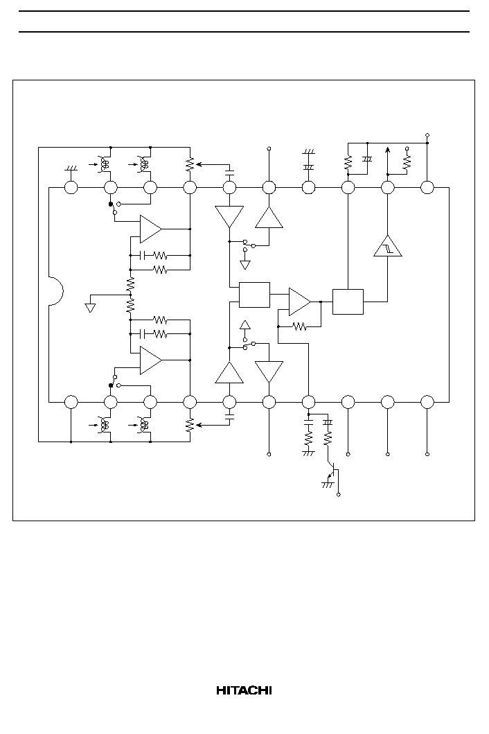
Block Diagram
+
-
+
20
19
18
17
16
15
14
MS
13
12
11
1
PBOUT(R)
V
CC
DV
CC
MS
MS DET
RIP
PBOUT(L)
TAI(L)
EQOUT(L)
RIN(L)
FIN(L)
GND
VREF
2
3
4
5
FIN(R)
RIN(R)
EQOUT(R)
TAI(R)
MS G
V
6
7
8
9
120
/70
Mute
FOR
/REV
10
-
+
LPF
RECT
I.A.
MA
S/R
+
+
I.A.
-
+

HA12231FP
5
Absolute Maximum Ratings (Ta = 25
∞
C)
Item
Symbol
Rating
Unit
Note
Supply voltage
V
CC
Max
15
V
Power dissipation
Pd
400
mW
Ta
85
∞
C
Operating temperature
Topr
-
40 to +85
∞
C
Storage temperature
Tstg
-
55 to +125
∞
C

HA12231FP
6
Electrical Characteristics
Item
Symbol
Test Condition
Application Terminal
IC Condition
Input
Specification
Output
Quiescent current
Input AMP. gain
Channel separation
PB-EQ gain
I
Q
Signal handling
G
V
IA
Vomax
T.H.D.
THD
G
V
EQ 1k
G
V
EQ 10k(1)
G
V
EQ 10k(2)
PB-EQ maximum output
V
OM
(Ta = 25
∞
C, V
CC
= 9 V, PBOUT Level = 450 mVrms (= 0 dB))
V
IH
PB-EQ THD
Noise voltage level converted
in input
THD-EQ
VN
MS sensing level
MS output leak current
MUTE attenuation
Control voltage
V
ON
MS output low level
V
OL
CT RL
I
OH
Mute
V
IL
Note:
1. V
CC
= 7.2 V
Min
22.5
12.0
50.0
37.0
33.0
29.0
300
3.5
-
18.0
70.0
-
0.2
Typ
23.5
13.0
0.05
60.0
40.0
36.0
32.0
600
6.0
0.1
1.2
-
14.0
1.0
0.0
80.0
R
5
2
2/3
2
2
2/3
2/3
2/3
5
5
5
L
16
19
19/18
19
19
19/18
19/18
16
16
16
R
6
6
15
4
4
4
19/18
41
7
4
4
6
6
12
6
L
15
51
6
6
1
5
51
6
6
1
5
15
6
17
17
17
17
17
15
15
12
15
11
12
12
8, 9,
10
Max
24.5
0.3
43.0
39.0
35.0
9
V
CC
0.5
2.0
-
10.0
1.5
2.0
1.0
Unit
Re-
mark
1
1
mA
dB
µ
A
dB
V
%
mVrms
dB
dB
dB
dB
%
dB
dB
V
µ
Vrms
fin(Hz)
Other
No signal
THD = 1%
Rg = 680
, Din-Audio Filter
TAI
TAI
TAI
FIN
FIN/RIN
FIN
FIN
FIN/RIN
0
0
12
0
0
0
120
µ
s
120
µ
s
70
µ
s
THD = 1%
No signal
FIN/RIN
FIN/RIN
0
(0)
TAI
TAI
TAI
0
12
INPUT
PBOUT
PBOUT
PBOUT
PBOUT
EQOUT
EQOUT
EQOUT
EQOUT
EQOUT
EQOUT
PBOUT
MSOUT
PBOUT
MSOUT
MSOUT
PBOUT
OUTPUT
1k
1k
1k
1k
1k
10k
10k
1k
1k
(1k)
5k
5k
1k
PBOUT
level(dB)
HA12231FP
7
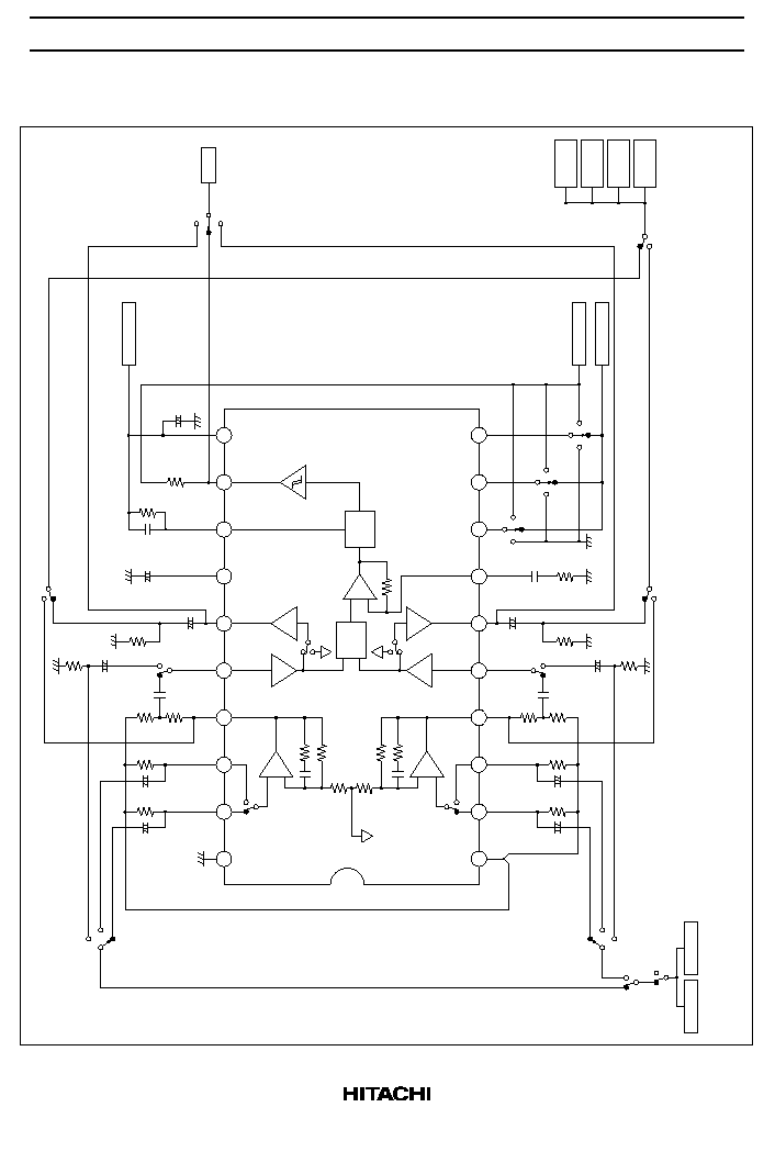
Test Circuit
+
-
+
20
19
18
17
16
15
14
MS
13
12
11
1
PBOUT(R)
V
CC
MS
MS DET
RIP
PBOUT(L)
TAI(L)
EQOUT(L)
RIN(L)
FIN(L)
GND
VREF
2
3
4
5
FIN(R)
RIN(R)
EQOUT(R)
TAI(R)
MS G
V
6
7
8
9
120
/70
Mute
FOR
/REV
10
-
+
LPF
R4
5.1k
R6
10k
R5
10k
PB
EQ
C2
22
µ
C3
0.1
µ
C12
0.1
µ
R2
680
SW5
FIN
SW9
SW7
Lch
Rch
SW12
R3
5.1k
R12
5.1k
R13
5.1k
R10
10k
SW6
SW8
PB
EQ
RECT
I.A.
R7
24k
MA
+
I.A.
-
+
+
C1
22
µ
R1
680
R15
680
R14
680
R9
330k
R8
3.9k
R11
10k
+
C4
0.47
µ
+
C5
2.2
µ
C10
2.2
µ
+
C6
0.01
µ
RIN
Rch
SW4
Lch
TAI
FIN
RIN
SW3
TAI
120
70
EXT
PBL
MS
PBR
SW13
SW10
OFF
ON
EXT
SW2
OFF
ON
SW1
SW11
FOR
REV
EXT
Notes:
1. Resistor tolerance
±
1%
2. Capacitor tolerance
±
1%
3. Unit R:
, C: F
AUDIO SG
DC SOURCE1
DC SOURCE2
DC SOURCE3
DC VM
AC VM1
+
+
+
C9
1
µ
C7
100
µ
C8
0.33
µ
C11
0.47
µ
+
C13
22
µ
C14
22
µ
Distortion
analyzer
Oscillo
scope
Noise
meter
NOISE METER
WITH CCIR/ARM FILTER
AND DIN/AUDIO FILTER
AC VM2

HA12231FP
8
Functional Description
Power Supply Range
HA12231FP is designed to operate on single supply only.
Table 1
Supply Voltage Range
Product
Single Supply
HA12231FP
7.2 V to 12.0 V
Reference Voltage
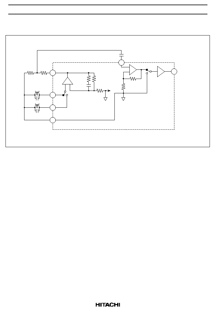
HA12231FP provides the reference voltage of half the supply voltage that is the signal grounds. As the
peculiarity of this device, the capacitor for the ripple filter is very small about 1/100 compared with their
usual value. The block diagram is shown as figure 1.
-
+
-
+
1
11 V
CC
RIP
C1
1
µ
14
+
20
to Line Amp.
VREF
MS block
: Internal reference voltage
Figure 1 The Block Diagram of Reference Supply Voltage

HA12231FP
9
Operating Mode Control
HA12231FP provides fully electronic switching circuits. And each operating mode control are controlled
by parallel data (DC voltage).
When a power supply of this IC is cut off, for a voltage, in addition to a mode control terminal even though
as do not destruct it, in series for resistance.
Table 2
Threshold Voltage (V
TH
)
Pin No.
Lo
Hi
Unit
Test Condition
8, 9, 10
-
0.2 to 1.0
3.5 to V
CC
V
Input Pin
Measure
V
Table 3
Switching Truth Table
Pin No.
Pin Name
Low
High
8
120
/70
120
µ
(Normal)
70
µ
(Metal or Chrome)
9
Mute
Mute OFF
Mute ON
10
FOR
/REV
Forward
Reverse
Notes: 1. Each pins are on pulled down with 100 k
internal resistor.
Therefore, it will be low-level when each pins are open.
2. Over shoot level and under shoot level of input signal must be the standardized.
(High: V
CC
, Low:
-
0.2 V)
3. Reducing pop noise is so much better for 10 k
to 22 k
resisitor and 1
µ
F to 22
µ
F capacitor
shown figure 2.
Input Pin
1 to 22
µ
F
MPU
10 to 22 k
+
Figure 2 Interface for Reduction of Pop Noise
HA12231FP
10
Input Block Diagram and Level Diagram
The each level shown above is typical value
when offering PBOUT level to PBOUT pin.
(EQ Amp. Gv = 40 dB, f = 1 kHz)
-
+
EQ Amp.
the other
channel
C1
0.1
µ
F
Input Amp.
60mVrms
(
-
22.2dBs)
EQOUT
TAI
30mVrms
(
-
28.2dBs)
FIN
PBIN
0.6mVrms
(-
62.2dBs)
RIN
VREF
PBOUT Level
HA12231FP: 450 mVrms (
-
4.7 dBs)
0dB
PBOUT
MUTE
-
+
R2
5.1k
23.5dB
R1
5.1k
Figure 3 Input Block Diagram
Adjustment of Playback Reference Operate Level
After replace R1 and R2 with a half-fix volume of 10 k
, adjust playback reference operate level.

HA12231FP
11
The Sensitivity Adjustment of Music Sensor
Adjusting MS Amp. gain by external resistor, the sensitivity of music sensor can set up. The music sensor
block diagram is shown in figure 4, and frequency response is shown in figure 5.
-
+
TAI(L)
TAI(R)
C1
0.33
µ
F
R1
330k
MS
MS Amp.
23.5dB
CEX2
REX2
REX1
MS DET
MS Gv
66.7k
90k
CEX1
+
LPF
RECT
V
CC
S/R
DV
CC
25kHz
-
6dB
23.5dB
+
GND
R
L
Micro
computer
16
7
13
12
20
5
33.3k
-
3.5dB
Figure 4 Music Sensor Block Diagram
G
V2
G
V1
10
100k
25k
10k
1k
f
3
f
4
f
2
f
1
f (Hz)
G
V
(dB)
100
Repeat mode (REP)
Search mode (SER)
Figure 5 Frequency Response

HA12231FP
12
1. Search mode
G
V1
= (23.5dB
-
3.5dB) + 20log 1 +
[dB]
90k
REX2
f
1
=
[Hz], f
2
= 25k [Hz]
1
2
CEX2
REX2
2. Repeat mode
G
V2
= (23.5dB
-
3.5dB) + 20log 1 +
[dB]
90k
REX1
f
3
=
[Hz], f
4
= 25k [Hz]
1
2
CEX1
REX1
The sensitivity of music sensor (S) is computed by the formula mentioned below.
S = 12.7
-
G
V
[dB]
S is 6 dB down in case of one-side channel.
Notes: 1. Search mode: G
V1
, Repeat mode: G
V2
2. Standard level of TAI pin (Dolby level correspondence) = 30 mVrms
3. Standard sensing level of music sensor = 130 mVrms
Item
REX1, 2
CEX1, 2
G
V1, 2
f
1, 3
f
2, 4
S
(one side
channel)
S
(both
channel)
Search mode
24 k
0.01
µ
F
33.5 dB
663 Hz
25 kHz
-
14.8 dB
-
20.8 dB
Repeat mode
2.4 k
1
µ
F
51.7 dB
66.3 Hz
25 kHz
-
33.0 dB
-
39.0 dB
Note:
This MS presented hysteresis lest MS(OUT) terminal should turn over again High level or Low level,
in case of thresh S level constantly.
Music Sensor Time Constant
1. Sensing no signal to signal (Attack) is determined by C1, 0.01
µ
F to 1
µ
F capacitor C1 can be
applicable.
2. Sensing signal to no signal (Recovery) is determined by C1 and R1, however preceding (1), 100 k
to 1
M
can be applicable.
Music Sensor Output (MS(OUT))
As for the internal circuit of music sensor block, music sensor output pin is connected to the collector of
NPN type directly, therefore, output level will be "high" when sensing no signal. And output level will be
"low" when sensing signal.
I
L
=
* MS(OUT)
LO
: Sensing signal (about 1V)
DV
CC
-
MS(OUT)
LO
*
R
L
Note:
Supply voltage of MS(OUT) pin must be less than V
CC
voltage.
HA12231FP
13
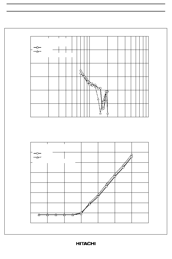
Characteristic Curves
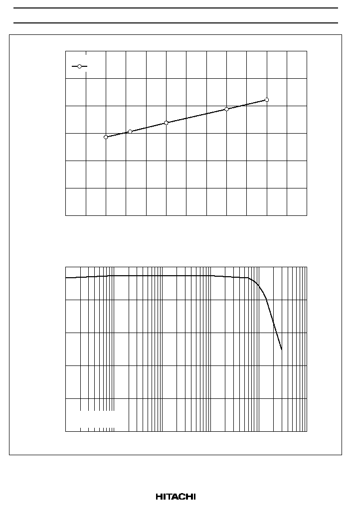
Transmission Frequency (MHz)
EQOUT Noise Output vs. Transmission Frequency
EQOUT Noise Output (dBs)
0
-
20
-
10
-
30
-
40
-
50
-
60
100
10000
1000
EQOUT(L), V
CC
= 9 V,
Vin = 0 dBm, 120
µ
s
toward Cellular phone noise
FIN(L)
RIN(L)
High Frequency Input Vin (dBm)
EQOUT Noise Output vs. Transmission Signal Input Level
EQOUT Noise Output (dBs)
0
-
20
-
10
-
30
-
40
-
60
-
80
-
70
-
50
-
50
-
40
-
30
-
10
0
10
20
-
20
EQOUT(L), V
CC
= 9 V,
120
µ
s, f = 900 MHz
toward Cellular phone noise
FIN(L)
RIN(L)
HA12231FP
14
Frequency (Hz)
Input Amp. Gain vs. Frequency
Gain (dB)
25
15
20
10
5
0
10
100
1k
100k
1M
10k
Supply Voltage (V)
Quiescent Current vs. Supply Voltage
Quiescent Current (mA)
7.0
6.0
6.5
5.5
5.0
4.0
4.5
4
6
10
12
14
16
8
No signal
70
µ
V
CC
= 9 V,
TAI
PBOUT

HA12231FP
15
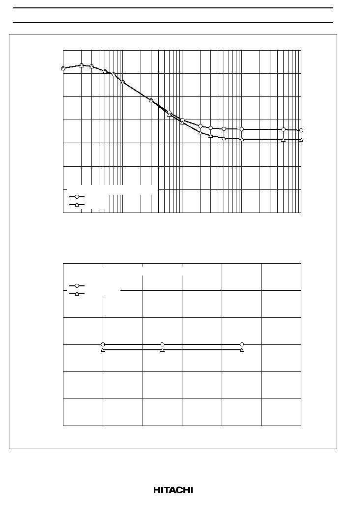
Output Level Vout (dB)
Total Harmonic Distortion vs. Output Level
T.H.D. (%)
10
1
0.01
0.1
-
15
-
10
-
5
5
10
15
20
0
Frequency (Hz)
Total Harmonic Distortion vs. Frequency
T.H.D. (%)
1
0.1
0.01
0.001
10
100
1k
100k
10k
TAI
PBOUT, 0 dB = 450 mVrms,
V
CC
= 9 V, Mute off
-
10 dB
0 dB
10 dB
TAI
PBOUT, 0 dB = 450 mVrms,
V
CC
= 9 V, Mute off
100 Hz
1 kHz
10 kHz
(30 kHz LPF)
(400 Hz HPF + 30 kHz LPF)
(400 Hz HPF + 80 kHz LPF)
30 kHz LPF
400 Hz HPF
+
30 kHz LPF
400 Hz HPF
+
80 kHz LPF

HA12231FP
16
Supply Voltage (V)
1
0.1
0.01
0.001
4
6
8
10
12
16
14
Supply Voltage (V)
Signal Handling
Vomax (dB)
30
25
20
10
0
5
15
4
6
10
12
14
16
8
TAI
PBOUT, 0 dB = 450 mVrms,
Mute off, f = 1 kHz, T.H.D. = 1%
PBOUT(L)
PBOUT(R)
TAI
PBOUT = 450 mVrms,
Mute off
100 Hz
1 kHz
10 kHz
(30 kHz LPF)
(400 Hz HPF + 30 kHz LPF)
(400 Hz HPF + 80 kHz LPF)
Total Harmonic Distortion vs. Supply Voltage
T.H.D. (%)
HA12231FP
17
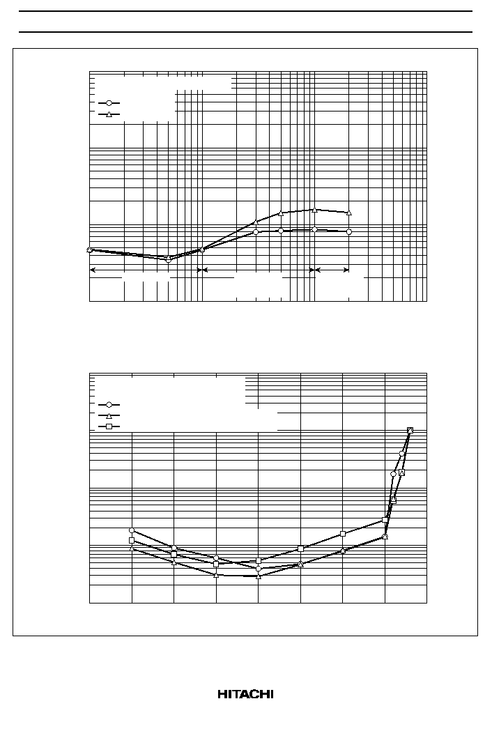
70
50
60
40
20
0
10
30
FIN
EQOUT, V
CC
= 9 V
120
µ
70
µ
Equalizer Amp. Gain vs. Frequency
EQ Gain (dB)
Frequency (Hz)
10
100
1k
100k
10k
Supply Voltage (V)
Signal to Noise Ratio vs. Supply Voltage
Signal to Noise Ratio (dB)
70
65
60
50
40
45
55
4
6
10
12
14
16
8
FIN
EQOUT, Vout = 0 dB = 60 mVrms,
DIN-AUDIO filter
120
µ
s
70
µ
s
HA12231FP
18
10
1
0.1
0.01
FIN
EQOUT, Vout = +20 dB,
0 dB = 60 mVrms
120
µ
s
70
µ
s
Total Harmonic Distortion vs. Frequency
T.H.D. (%)
Frequency (Hz)
100
1k
100k
10k
30 kHz LPF
400 Hz HPF
+
30 kHz LPF
400 Hz HPF
+
80 kHz LPF
100
1
10
0.1
0.01
FIN
EQOUT, 0 dB = 60 mVrms,
V
CC
= 9 V
Total Harmonic Distortion vs. Output Level (120
µ
s)
T.H.D. (%)
Output Level Vout (dB)
-
5
10
35
30
25
15
5
0
20
100 Hz
1 kHz
10 kHz
(30 kHz LPF)
(400 Hz HPF + 30 kHz LPF)
(400 Hz HPF + 80 kHz LPF)

HA12231FP
19
100
1
10
0.1
0.01
FIN
EQOUT, 0 dB = 60 mVrms,
V
CC
= 9 V
Total Harmonic Distortion vs. Output Level (70
µ
s)
T.H.D. (%)
Output Level Vout (dB)
-
5
10
35
30
25
15
5
0
20
100 Hz
1 kHz
10 kHz
(30 kHz LPF)
(400 Hz HPF + 30 kHz LPF)
(400 Hz HPF + 80 kHz LPF)
Supply Voltage (V)
10
1
0.1
0.01
4
6
8
10
12
16
14
FIN
EQOUT, Vout = 60 mVrms,
V
CC
= 9 V
100 Hz
1 kHz
10 kHz
(30 kHz LPF)
(400 Hz HPF + 30 kHz LPF)
(400 Hz HPF + 80 kHz LPF)
Total Harmonic Distortion vs. Supply Voltage (120
µ
s)
T.H.D. (%)
HA12231FP
20
Supply Voltage (V)
10
1
0.1
0.01
4
6
8
10
12
16
14
FIN
EQOUT, Vout = 60 mVrms,
V
CC
= 9 V
100 Hz
1 kHz
10 kHz
(30 kHz LPF)
(400 Hz HPF + 30 kHz LPF)
(400 Hz HPF + 80 kHz LPF)
Total Harmonic Distortion vs. Supply Voltage (70
µ
s)
T.H.D. (%)
Supply Voltage (V)
Signal Handling
Vomax (dB)
45
40
35
25
15
20
30
4
6
10
12
14
16
8
FIN, RIN
EQOUT, 120
µ
s, 0 dB = 60 mVrms,
f = 1 kHz, T.H.D. = 1%
FIN
RIN

HA12231FP
21
FIN
PBOUT, Vout = 12 dB (0 dB = 450 mVrms),
80 kHz LPF
L
R
R
L
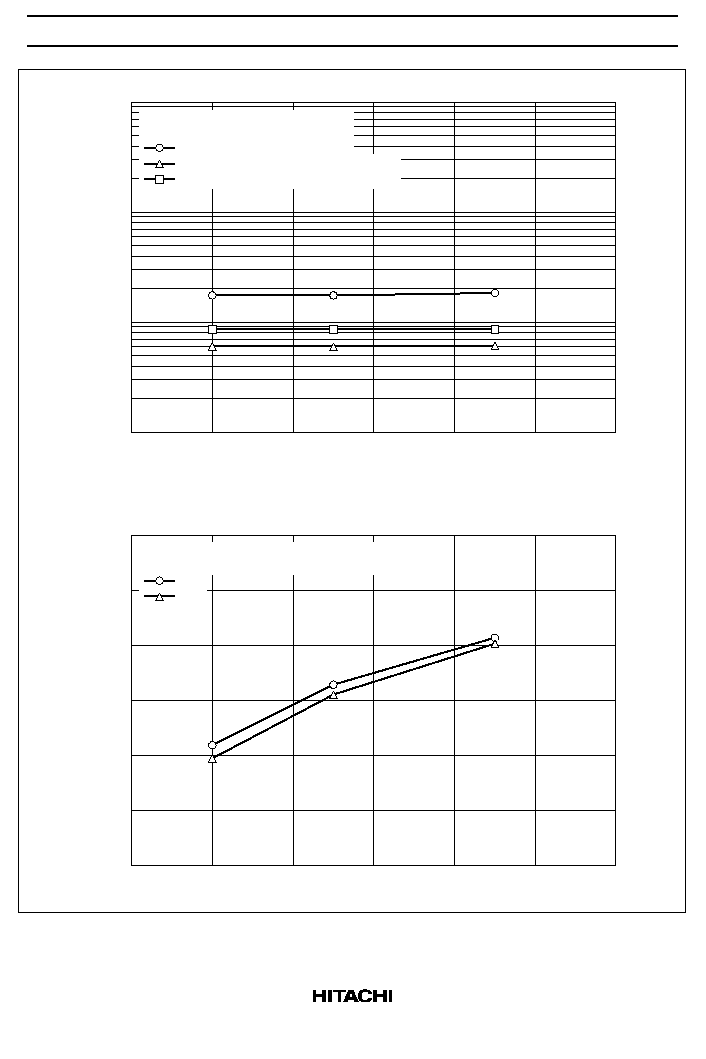
Crosstalk vs. Frequency (CTRL)
Supply Voltage (V)
Signal Handling
Vomax (dB)
45
40
35
25
15
20
30
4
6
10
12
14
16
8
FIN, RIN
EQOUT, 70
µ
s, 0 dB = 60 mVrms,
f = 1 kHz, T.H.D. = 1%
FIN
RIN
Frequency (Hz)
10
100
1k
100k
10k
0
-
20
-
30
-
10
-
40
-
60
-
80
-
70
-
50
Crosstalk (dB)

HA12231FP
22
MS Amp. Sensitivity vs. Frequency
Frequency (Hz)
10
100
1k
100k
10k
10
0
-
20
-
30
-
10
-
40
MS Sensing Level (dB)
RIN
PBOUT, Vout = 12 dB (0 dB = 450 mVrms),
80 kHz LPF
L
R
R
L
Crosstalk vs. Frequency (CTRL)
Frequency (Hz)
10
100
1k
100k
10k
0
-
20
-
30
-
10
-
40
-
60
-
80
-
70
-
50
Crosstalk (dB)
TAI
PBOUT, V
CC
= 9 V,
0 dB = 450 mVrms
SER L
H
SER H
L
REP L
H
REP H
L

HA12231FP
23
Resistance R10 (
)
No-Signal Sensing Time vs. Resistance
No-Signal Sensing Time (ms)
1000
10
100
1
10M
100k
1M
10k
PBOUT
MSOUT
1000
10
100
0.1
1
Capacitance C8 (
µ
F)
Signal Sensing Time vs. Capacitance
Signal Sensing Time (ms)
0.001
0.01
10
1
0.1
PBOUT
MSOUT
TAI
PBOUT, V
CC
= 9 V,
f = 5 kHz, MSOUT L
H
SER 0 dB
TAI
PBOUT, V
CC
= 9 V,
f = 5 kHz, MSOUT H
L
SER 0 dB

HA12231FP
24
Package Dimensions
Hitachi Code
JEDEC
EIAJ
Mass (reference value)
FP-20DA
--
Conforms
0.31 g
Unit: mm
*Dimension including the plating thickness
Base material dimension
*0.42
±
0.08
0.12
0.15
M
20
10
1
*0.22
±
0.05
0.80 Max
11
12.6
5.5
2.20 Max
13 Max
0
∞
≠ 8
∞
0.70
±
0.20
+ 0.20
≠ 0.30
7.80
1.27
0.10
±
0.10
1.15
0.40
±
0.06
0.20
±
0.04

HA12231FP
25
Cautions
1. Hitachi neither warrants nor grants licenses of any rights of Hitachi's or any third party's patent,
copyright, trademark, or other intellectual property rights for information contained in this document.
Hitachi bears no responsibility for problems that may arise with third party's rights, including
intellectual property rights, in connection with use of the information contained in this document.
2. Products and product specifications may be subject to change without notice. Confirm that you have
received the latest product standards or specifications before final design, purchase or use.
3. Hitachi makes every attempt to ensure that its products are of high quality and reliability. However,
contact Hitachi's sales office before using the product in an application that demands especially high
quality and reliability or where its failure or malfunction may directly threaten human life or cause risk
of bodily injury, such as aerospace, aeronautics, nuclear power, combustion control, transportation,
traffic, safety equipment or medical equipment for life support.
4. Design your application so that the product is used within the ranges guaranteed by Hitachi particularly
for maximum rating, operating supply voltage range, heat radiation characteristics, installation
conditions and other characteristics. Hitachi bears no responsibility for failure or damage when used
beyond the guaranteed ranges. Even within the guaranteed ranges, consider normally foreseeable
failure rates or failure modes in semiconductor devices and employ systemic measures such as fail-
safes, so that the equipment incorporating Hitachi product does not cause bodily injury, fire or other
consequential damage due to operation of the Hitachi product.
5. This product is not designed to be radiation resistant.
6. No one is permitted to reproduce or duplicate, in any form, the whole or part of this document without
written approval from Hitachi.
7. Contact Hitachi's sales office for any questions regarding this document or Hitachi semiconductor
products.
Hitachi, Ltd.
Semiconductor & Integrated Circuits.
Nippon Bldg., 2-6-2, Ohte-machi, Chiyoda-ku, Tokyo 100-0004, Japan
Tel: Tokyo (03) 3270-2111 Fax: (03) 3270-5109
Copyright
©
Hitachi, Ltd., 2001. All rights reserved. Printed in Japan.
Hitachi Asia Ltd.
Hitachi Tower
16 Collyer Quay #20-00,
Singapore 049318
Tel : <65>-538-6533/538-8577
Fax : <65>-538-6933/538-3877
URL : http://www.hitachi.com.sg
URL
NorthAmerica
: http://semiconductor.hitachi.com/
Europe
: http://www.hitachi-eu.com/hel/ecg
Asia
: http://sicapac.hitachi-asia.com
Japan
: http://www.hitachi.co.jp/Sicd/indx.htm
Hitachi Asia Ltd.
(Taipei Branch Office)
4/F, No. 167, Tun Hwa North Road,
Hung-Kuo Building,
Taipei (105), Taiwan
Tel : <886>-(2)-2718-3666
Fax : <886>-(2)-2718-8180
Telex : 23222 HAS-TP
URL : http://www.hitachi.com.tw
Hitachi Asia (Hong Kong) Ltd.
Group III (Electronic Components)
7/F., North Tower,
World Finance Centre,
Harbour City, Canton Road
Tsim Sha Tsui, Kowloon,
Hong Kong
Tel : <852>-(2)-735-9218
Fax : <852>-(2)-730-0281
URL : http://www.hitachi.com.hk
Hitachi Europe Ltd.
Electronic Components Group.
Whitebrook Park
Lower Cookham Road
Maidenhead
Berkshire SL6 8YA, United Kingdom
Tel: <44> (1628) 585000
Fax: <44> (1628) 585160
Hitachi Europe GmbH
Electronic Components Group
Dornacher Straße 3
D-85622 Feldkirchen, Munich
Germany
Tel: <49> (89) 9 9180-0
Fax: <49> (89) 9 29 30 00
Hitachi Semiconductor
(America) Inc.
179 East Tasman Drive,
San Jose,CA 95134
Tel: <1> (408) 433-1990
Fax: <1>(408) 433-0223
For further information write to:
Colophon 2.0