 | –≠–ª–µ–∫—Ç—Ä–æ–Ω–Ω—ã–π –∫–æ–º–ø–æ–Ω–µ–Ω—Ç: HA13118 | –°–∫–∞—á–∞—Ç—å:  PDF PDF  ZIP ZIP |
HA13118
18 W BTL Audio Power Amplifier
ADE-207-329 (Z)
1st Edition
Dec. 2000
Description
The HA13118 is power IC designed for component car stereo amplifiers. At 13.2 V to 4
load, this power
IC provides an output power of 18W with 10% distortion.
It is easy to design as this IC employs internal each protection circuit and the new small package.
Features
∑
Small outline package, easy to mount
∑
Internal each protection circuits
Surge protection circuit
Thermal shut-down circuit
Ground fault protection circuit
Power supply fault protection circuit
Absolute Maximum Ratings (Ta = 25∞C)
Item
Symbol
Rating
Unit
Note
Operating supply voltage
V
CC
18
V
DC supply voltage
V
CC
(DC)
26
V
1
Peak supply voltage
V
CC
(peak)
50
V
2
Output current
Io (peak)
4
A
Power dissipation
P
T
15
W
Thermal resistance
j ≠ c
3.5
∞C/W
Junction temperature
Tj
150
∞C
Operating temperature
Topr
≠30 to +80
∞C
Storage temperature
Tstg
≠55 to +125
∞C
Notes: 1. Value at t = 30 sec.
2. Value at width tw = 200 ms and rise time tr = 1 ms.
HA13118
Rev.1, Dec. 2000, page 2 of 8
Electrical Characteristics (V
CC
= 13.2 V, f = 1 kHz, R
L
= 4
, Ta = 25 ∞C)
Item
Symbol
Min
Typ
Max
Unit
Test Conditions
Quiescent current
I
Q
40
80
160
mA
Vin = 0
Input bias voltage
V
B
--
20
40
mV
Vin = 0
Output offset voltage
V
Q
--
--
+330
mV
Vin = 0
Voltage gain
G
V
53
55
57
dB
Vin = ≠55 dBm
Output power
Pout
15
18
--
W
THD = 10 %
R
L
= 4
--
11
--
R
L
= 8
Total harmonic distortion
THD
--
0.2
1.0
%
Pout = 1.5 W
Output noise voltage
WBN
--
1.0
2.0
mV
Rg = 10 k
, BW = 20 Hz
20 kHz
Supply voltage rejection
ratio
SVR
33
44
--
dB
f = 500 Hz
Input resistance
Rin
20
30
40
k
Rolloff frequency
f
L
--
20
--
Hz
Gv = ≠3 dB
Low
f
H
10
20
40
kHz
from f = 1 kHz Ref. High
HA13118
Rev.1, Dec. 2000, page 3 of 8
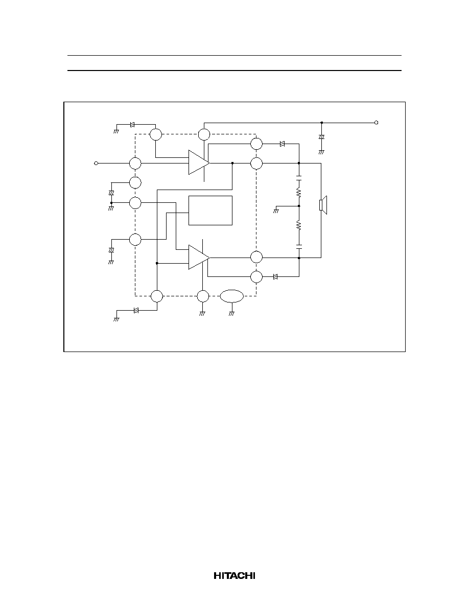
Block Diagram
ASO Protect
Surge Protect
TSD
Amp1
Amp2
5
TAB
12
6
10
8
15
14
13
1
3
2
4
+
+
+
C
2,200
(16 V)
107
µ
+
C
100 (10 V)
108
µ
≠
+
C
100 (6.3 V)
101
µ
+
C
100 F
(6.3 V)
103
µ
+
C
10
(6.3 V)
104
µ
+
C
100 (6.3V)
102
µ
+
C
100
(10 V)
109
µ
C
0.1
106
µ
R
2.2
102
R
2.2
101
C
0.1
105
µ
R
4 - 8
L
V
CC
Input
≠
≠
≠
≠
≠
≠
≠
≠
Note:
C
105
, C
106
must be non secondary resonance type (non inductive) polyester film capacitor for keeping
stability.
Figure 1 Typical Application Circuit
HA13118
Rev.1, Dec. 2000, page 4 of 8
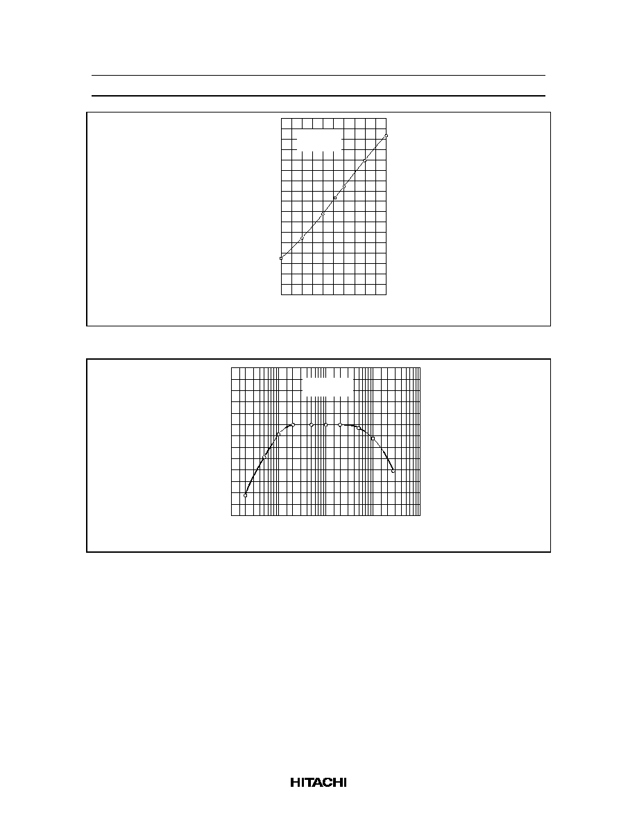
8
10
12
14
16
18
0
10
20
30
Supply voltage V (V)
CC
Output power P (W)
out
R = 4
f = 1 kHz
L
Figure 2 Output Power vs. Supply Voltage
50
55
60
50
20
100 200 500 1 k 2 k
5 k 10 k 20 k 50 k 100 k
V = 13.2 V
R = 4
CC
L
Frequency f (Hz)
Gv (dB)
10
Figure 3 Voltage Gain vs. Frequency
HA13118
Rev.1, Dec. 2000, page 5 of 8
P = 8 W
out
P = 15 W
out
20
50 100 200 500 1 k 2 k
5 k 10 k 20 k 50 k
0.02
0.05
0.1
0.2
0.5
1.0
2
5
10
Frequency f (Hz)
Total Harmonic Distortion THD (%)
V = 13.2 V
R = 4
CC
L
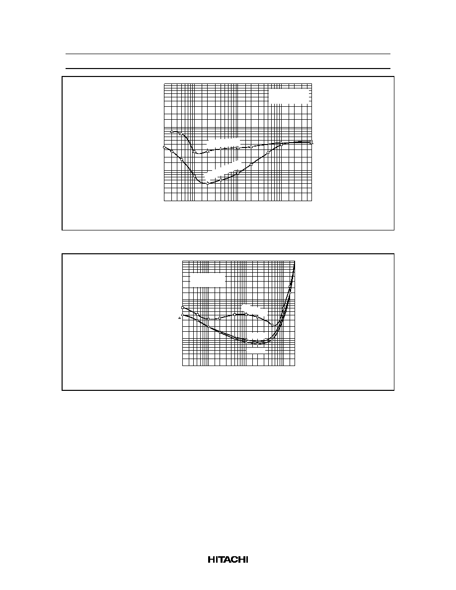
Figure 4 Total Harmonic Distortion vs. Frequency
0.02
Total Harmonic Distortion THD (%)
0.02
V = 13.2 V
R = 4
L
CC
0.05 0.1 0.2
0.5 1.0
2
5
10
20
0.05
0.1
0.2
0.5
1.0
2
5
10
f = 10 kHz
100 Hz
Output Power P (W)
out
1 kHz
Figure 5 Total Harmonic Distortion vs. Output Power