 | –≠–ª–µ–∫—Ç—Ä–æ–Ω–Ω—ã–π –∫–æ–º–ø–æ–Ω–µ–Ω—Ç: HA13153A | –°–∫–∞—á–∞—Ç—å:  PDF PDF  ZIP ZIP |

HA13153A, HA13154A
15 W
◊
4-Channel BTL Power IC
ADE-207-181B (Z)
3rd Edition
Jul. 1999
Description
The HA13153A/HA13154A is high output and low distortion 4 ch BTL power IC designed for digital car
audio.
At 13.2 V to 4
load, this power IC provides output power 15 W with 10% distortion.
Function
∑
4 ch BTL power amplifiers
∑
Built-in standby circuit
∑
Built-in muting circuit
∑
Built-in protection circuit (surge, T.S.D, and ASO)
Features
∑
Few external parts lead to compact set-area possibility than HA13150A/HA13151/HA13152 (C: 3, R:
1)
∑
Popping noise minimized
∑
Low output noise
∑
Built-in high reliability protection circuit
∑
Pin to pin with HA13150A/HA13151/HA13152/HA13155
HA13153A, HA13154A
2
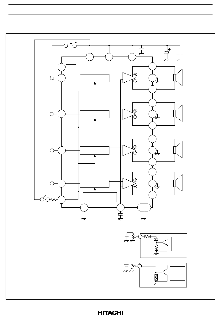
Block Diagram
STBY
2
IN-1
1
11
IN-2
IN-3
13
23
IN-4
MUTE
10
R1
7.5 k
12
22
TAB
C3
10
µ
/10 V
14
18
6
IN V
CC
PV
CC
1
Buffer & Mute-1
Buffer & Mute-2
Buffer & Mute-3
Buffer & Mute-4
Protector
(ASO, Surge, TSD)
Amp-1
Amp-2
Amp-3
Amp-4
V
CC
13.2 V
C1
4400
µ
/16 V
3
4
5
7
8
9
15
16
17
19
20
21
Unit
R:
C: F
2
5 V
5 V
37.5 k
23.5 k
25 k
Q1 ON
BIAS ON
Q2 ON
MUTE ON
10
C2 should be polyester film capacitors with no secondary resonance (non-inductive),
to assure stable operation.
Notes:
Standby
Power is turned on when a signal of
3.5 V or 0.05 mA is impressed at pin 2.
When pin 2 is open or connected to
GND, standby is turned on (output off).
1.
2.
3.
C2
0.1
µ
/16 V
PV
CC
2
Muting
Muting is turned off (output on) when
a signal of 3.5 V or 0.2 mA is impressed
at pin 10.
When pin 10 is open or connected to
GND, muting is turned on (output off).
TAB (header of IC) connected to GND.

HA13153A, HA13154A
3
Absolute Maximum Ratings
Item
Symbol
Rating
Unit
Operating supply voltage
V
CC
18
V
Supply voltage when no signal*
1
V
CC
(DC)
26
V
Peak supply voltage*
2
V
CC
(PEAK)
50
V
Output current*
3
I
O
(PEAK)
3
A
Power dissipation*
4
P
T
83
W
Junction temperature
Tj
150
∞
C
Operating temperature
Topr
≠30 to +85
∞
C
Storage temperature
Tstg
≠55 to +125
∞
C
Notes: 1. Tolerance within 30 seconds.
2. Tolerance in surge pulse waveform.
3. Value per 1 channel.
4. Value when attached on the infinite heat sink plate at Ta = 25
∞
C.
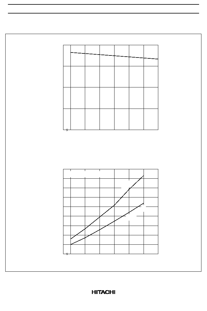
The derating carve is as shown in the graph below.
100
50
0
25
50
85
100
150
Ambient temperature Ta (
∞
C)
Power dissipation P
T
(W)
A: When heat sink is infinite (
j-a = 1.5
∞
C/W)
B: When
f (thermal resistance of heat sink) = 3
∞
C/W
(
j-a = 4.5
∞
C/W)
B
83 W
28 W
A

HA13153A, HA13154A
4
Electrical Characteristics (V
CC
= 13.2 V, f = 1 kHz, R
L
= 4
, Rg = 600
, Ta = 25
∞
C)
HA13153A
Item
Symbol
Min
Typ
Max
Unit
Test Conditions
Quiescent current
I
Q
1
--
350
--
mA
Vin = 0
Output offset voltage
V
Q
≠300
0
+300
mV
Gain
G
V
30.5
32
33.5
dB
Gain difference between
channels
G
V
≠1.0
0
+1.0
dB
Rated output power
Po
--
15
--
W
V
CC
= 13.2 V
THD = 10%, R
L
= 4
Max output power
Pomax
--
25
--
W
V
CC
= 13.7 V, R
L
= 4
Total harmonic distortion
T.H.D.
--
0.02
--
%
Po = 3 W
Output noise voltage
WBN
--
0.15
--
mVrms
Rg = 0
BW = 20 to 20 kHz
Ripple rejection
SVR
--
55
--
dB
Rg = 600
, f = 120 Hz
Channel cross talk
C.T.
--
70
--
dB
Rg = 600
Vout = 0 dBm
Input impedance
Rin
--
25
--
k
Standby current
I
Q
2
--
--
10
µ
A
Standby control voltage
(high)
V
STH
3.5
--
V
CC
V
Standby control voltage
(low)
V
STL
0
--
1.5
V
Muting control voltage
(high)
V
MH
3.5
--
V
CC
V
Muting control voltage
(low)
V
ML
0
--
1.5
V
Muting attenuation
ATTM
--
70
--
dB
Vout = 0 dBm

HA13153A, HA13154A
5
HA13154A
Item
Symbol
Min
Typ
Max
Unit
Test Conditions
Quiescent current
I
Q
1
--
350
--
mA
Vin = 0
Output offset voltage
V
Q
≠300
0
+300
mV
Gain
G
V
38.5
40
41.5
dB
Gain difference between
channels
G
V
≠1.0
0
+1.0
dB
Rated output power
Po
--
15
--
W
V
CC
= 13.2 V
THD = 10%, R
L
= 4
Max output power
Pomax
--
25
--
W
V
CC
= 13.7 V, R
L
= 4
Total harmonic distortion
T.H.D.
--
0.02
--
%
Po = 3 W
Output noise voltage
WBN
--
0.25
--
mVrms
Rg = 0
BW = 20 to 20 kHz
Ripple rejection
SVR
--
45
--
dB
Rg = 600
, f = 120 Hz
Channel cross talk
C.T.
--
60
--
dB
Rg = 600
Vout = 0 dBm
Input impedance
Rin
--
25
--
kW
Standby current
I
Q
2
--
--
10
µ
A
Standby control voltage
(high)
V
STH
3.5
--
V
CC
V
Standby control voltage
(low)
V
STL
0
--
1.5
V
Muting control voltage
(high)
V
MH
3.5
--
V
CC
V
Muting control voltage
(low)
V
ML
0
--
1.5
V
Muting attenuation
ATTM
--
60
--
dB
Vout = 0 dBm
HA13153A, HA13154A
6
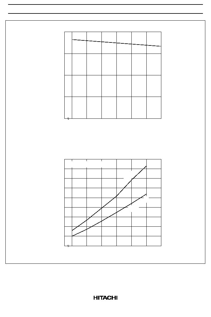
Characteristics Curve
8
10
12
14
16
18
20
400
300
200
100
Supply Voltage V
CC
(V)
Quiescent current I
Q
(mA)
0
0
Quiescent current vs. Supply Voltage (HA13153A)
8
10
12
14
16
18
20
45
35
20
15
Supply Voltage V
CC
(V)
Output Power Po, Pomax (W)
0
0
Output Power vs. Supply Voltage (HA13153A)
40
30
25
10
5
Po(THD = 10 %)
Pomax
R
L
= 4
, f = 1 kHz

HA13153A, HA13154A
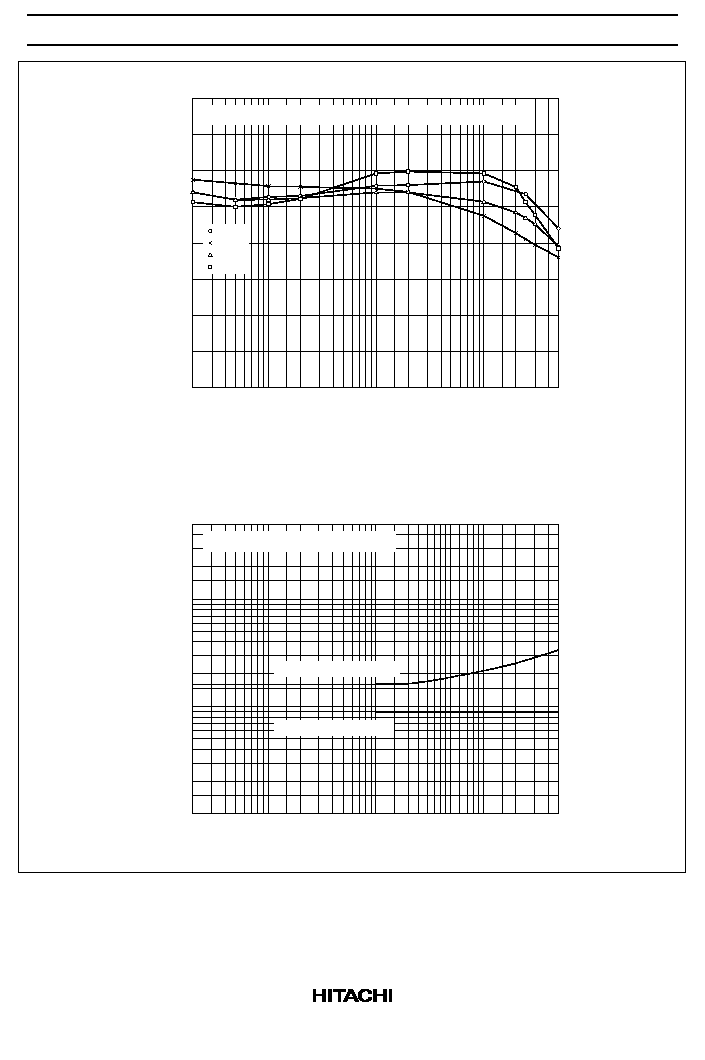
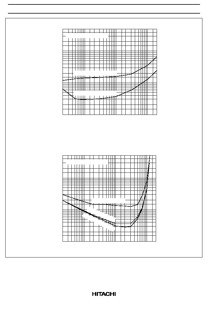
7
20
50
100 200
500
1k
2k
5k
5
Frequency f (Hz)
Total Harmonic Distortion THD (%)
10k 20k
2
0.5
1
0.2
0.1
0.01
0.02
0.05
V
CC
= 13.2 V, R
L
= 4
Total Harmonic Distortion vs. Frequency (HA13153A)
Po = 3.0 W (Ch1≠Ch4)
Po = 8.0 W (Ch1≠Ch4)
0.02
0.05 0.1
0.2
0.5
1
2
5
5
Output Power Po (W)
Total Harmonic Distortion THD (%)
10
20
2
0.5
1
0.2
0.1
0.01
0.02
0.05
V
CC
= 13.2 V, R
L
= 4
, f = 1 kHz
Total Harmonic Distortion vs. Output Power (HA13153A)
10 kHz (Ch1≠Ch4)
1 kHz (Ch1≠Ch4)
100 Hz (Ch1≠Ch4)

HA13153A, HA13154A
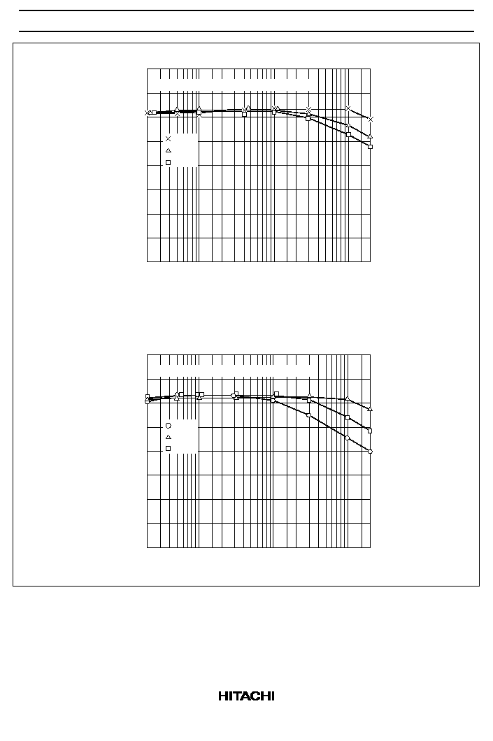
8
20
50
100 200
500
1k
2k
5k
80
Frequency f (Hz)
Crosstalk C
T
(dB)
10k 20k
70
50
60
40
30
0
10
20
Input Ch1, V
CC
= 13.2 V, Vout = 0 dBm
Crosstalk vs. Frequency (HA13153A) (1)
Ch2
Ch3
Ch4
20
50
100 200
500
1k
2k
5k
80
Frequency f (Hz)
Crosstalk C
T
(dB)
10k 20k
70
50
60
40
30
0
10
20
Input Ch2, V
CC
= 13.2 V, Vout = 0 dBm
Crosstalk vs. Frequency (HA13153A) (2)
Ch1
Ch3
Ch4

HA13153A, HA13154A
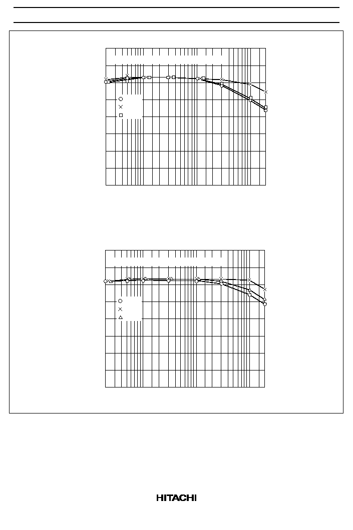
9
20
50
100 200
500
1k
2k
5k
80
Frequency f (Hz)
Crosstalk C
T
(dB)
10k 20k
70
50
60
40
30
0
10
20
Input Ch3, V
CC
= 13.2 V, Vout = 0 dBm
Crosstalk vs. Frequency (HA13153A) (3)
Ch1
Ch2
Ch4
20
50
100 200
500
1k
2k
5k
80
Frequency f (Hz)
Crosstalk C
T
(dB)
10k 20k
70
50
60
40
30
0
10
20
Input Ch4, V
CC
= 13.2 V, Vout = 0 dBm
Crosstalk vs. Frequency (HA13153A) (4)
Ch1
Ch2
Ch3
HA13153A, HA13154A
10
20
50
100 200
500
1k
2k
5k
80
Supply Voltage Rejection Ratio SVR (dB)
10k 20k
70
50
60
40
30
0
10
20
V
CC
= 13.2 V, RL = 4
, Vripple = 0 dBm, Rg = 620
Ch1
Ch2
Ch3
Ch4
50k
Supply Voltage Rejection Ratio vs. Frequency (HA13153A)
Frequency f (Hz)
Mute OFF Ch1≠Ch4
Mute ON Ch1≠Ch4
20
50
100 200
500
1k
2k
5k
5
Wide Band Noise WBN (mV)
10k 20k
2
0.5
1
0.2
0.1
0.01
0.02
0.05
50k
Wide Band Noise vs. Signal Source Resistance (HA13153A)
Signal Source Resistance Rg (
)
V
CC
= 13.2 V, R
L
= 4
, Vin = 0

HA13153A, HA13154A
11
0.02
0.05 0.1
0.2
0.5
1
2
5
500
Power Dissipation P
T
(W)
10
20
200
50
100
20
10
1
2
5
Power Dissipation vs. Output Power (HA13153A)
Output Power Po (W)
R
L
= 4
, f = 1 kHz, 1ch operation
V
CC
= 16 V (Ch1≠Ch4)
V
CC
= 13.2 V (Ch1≠Ch4)
20
50
100 200
500
1k
2k
5k
15
Frequency f (Hz)
Power Dissipation P
T
(W)
10k 20k
10
5
0
Power Dissipation vs. Frequency (HA13153A)
V
CC
= 13.2 V, R
L
= 4
, Po = 10 W, 1ch operation
Ch1≠Ch4
HA13153A, HA13154A
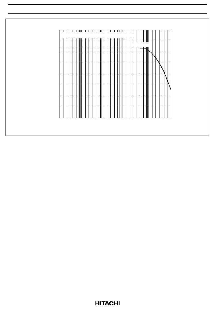
12
40
35
30
25
20
15
10
5
0
Ch1≠Ch4
10
Gain G
V
(dB)
Gain vs. Frequency (HA13153A)
Frequency f (Hz)
V
CC
= 13.2 V, R
L
= 4
, V
OUT
= 0 dBm
20
50 100 200 500 1k 2k
5k 10k 20k 50k 100k200k 500k 1M
HA13153A, HA13154A
13
8
10
12
14
16
18
20
400
300
200
100
0
0
8
10
12
14
16
18
20
45
35
20
15
0
0
40
30
25
10
5
Po(THD = 10 %)
Pomax
R
L
= 4
, f = 1 kHz
Supply Voltage V
CC
(V)
Quiescent current I
Q
(mA)
Quiescent current vs. Supply Voltage (HA13154A)
Supply Voltage V
CC
(V)
Output Power Po, Pomax (W)
Output Power vs. Supply Voltage (HA13154A)
HA13153A, HA13154A
14
5
2
1
0.2
0.1
0.05
0.02
0.01
20
50
100 200
500 1 k
2 k
20 k
10 k
5 k
0.5
P
O
= 3.0 W (Ch1≠Ch4)
P
O
= 8.0 W (Ch1≠Ch4)
V
CC
= 13.2 V, R
L
= 4
5
2
1
0.2
0.1
0.05
0.02
0.01
0.02
0.05 0.1
0.2
0.5
1
2
20
10
5
0.5
1 kHz (Ch1≠Ch4)
100 kHz (Ch1-Ch4)
10 kHz (Ch1≠Ch4)
V
CC
= 13.2 V, R
L
= 4
Frequency f (Hz)
Total Harmonic Distortion THD (%)
Total Harmonic Distortion vs. Frequency (HA13154A)
Output Power Po (W)
Total Harmonic Distortion THD (%)
Total Harmonic Distortion vs. Output Power (HA13154A)
HA13153A, HA13154A
15
80
70
60
40
30
20
10
0
20
50
100 200
500
1 k
2 k
20 k
10 k
5 k
50
Input Ch1, V
CC
= 13.2 V, Vout = 0 dB
Ch2
Ch3
Ch4
80
70
60
40
30
20
10
0
20
50
100 200
500 1 k
2 k
20 k
10 k
5 k
50
Input Ch2, V
CC
= 13.2 V, Vout = 0 dB
Ch1
Ch3
Ch4
Frequency f (Hz)
Crosstalk C
T
(dB)
Crosstalk vs. Frequency (HA13154A) (1)
Frequency f (Hz)
Crosstalk C
T
(dB)
Crosstalk vs. Frequency (HA13154A) (2)
HA13153A, HA13154A
16
80
70
60
40
30
20
10
0
20
50
100 200
500 1 k
2 k
20 k
10 k
5 k
50
Input Ch3, V
CC
= 13.2 V, Vout = 0 dB
Ch1
Ch2
Ch4
80
70
60
40
30
20
10
0
20
50
100 200
500 1 k
2 k
20 k
10 k
5 k
50
Input Ch4, V
CC
= 13.2 V, Vout = 0 dB
Ch1
Ch2
Ch3
Frequency f (Hz)
Crosstalk C
T
(dB)
Crosstalk vs. Frequency (HA13154A) (3)
Frequency f (Hz)
Crosstalk C
T
(dB)
Crosstalk vs. Frequency (HA13154A) (4)

HA13153A, HA13154A
17
80
70
60
40
30
20
10
0
20
50
100 200
500 1 k
2 k
20 k 50 k
10 k
5 k
50
V
CC
= 13.2 V, R
L
= 4
, Vripple = 0 dB
Ch1
Ch2
Ch3
Ch4
5
2
1
0.5
0.2
0.1
0.05
0.02
0.01
20
50 100 200
500 1 k
2 k
20 k
50 k
10 k
5 k
Mute OFF Ch1≠Ch4
Mute ON Ch1≠Ch4
V
CC
= 13.2 V, R
L
= 4
, Vin = 0
Supply Voltage Rejection Ratio SVR (dB)
Supply Voltage Rejection Ratio vs. Frequency (HA13154A)
Frequency f (Hz)
Wide Band Noise WBN (mV)
Wide Band Noise vs. Signal Source Resistance (HA13154A)
Signal Source Resistance Rg (
)

HA13153A, HA13154A
18
0.02
0.05 0.1
0.2
0.5
1
2
5
500
10
20
200
50
100
20
10
1
2
5
R
L
= 4
, f = 1 kHz, 1ch operation
V
CC
= 16 V (Ch1≠Ch4)
V
CC
= 13.2 V (Ch1≠Ch4)
20
50
100 200
500
1k
2k
5k
15
10k 20k
10
5
0
V
CC
= 13.2 V, R
L
= 4
, Po = 10 W, 1ch operation
Ch1≠Ch4
Power Dissipation P
T
(W)
Power Dissipation vs. Output Power (HA13154A)
Output Power Po (W)
Frequency f (Hz)
Power Dissipation P
T
(W)
Power Dissipation vs. Frequency (HA13154A)

HA13153A, HA13154A
19
40
35
30
25
20
15
10
Ch1≠Ch4
10
V
CC
= 13.2 V, R
L
= 4
, V
OUT
= 0 dBm
20
50 100 200 500 1k 2k
5k 10k 20k 50k 100k200k 500k 1M
45
50
Gain G
V
(dB)
Gain vs. Frequency (HA13154A)
Frequency f (Hz)
HA13153A, HA13154A
20
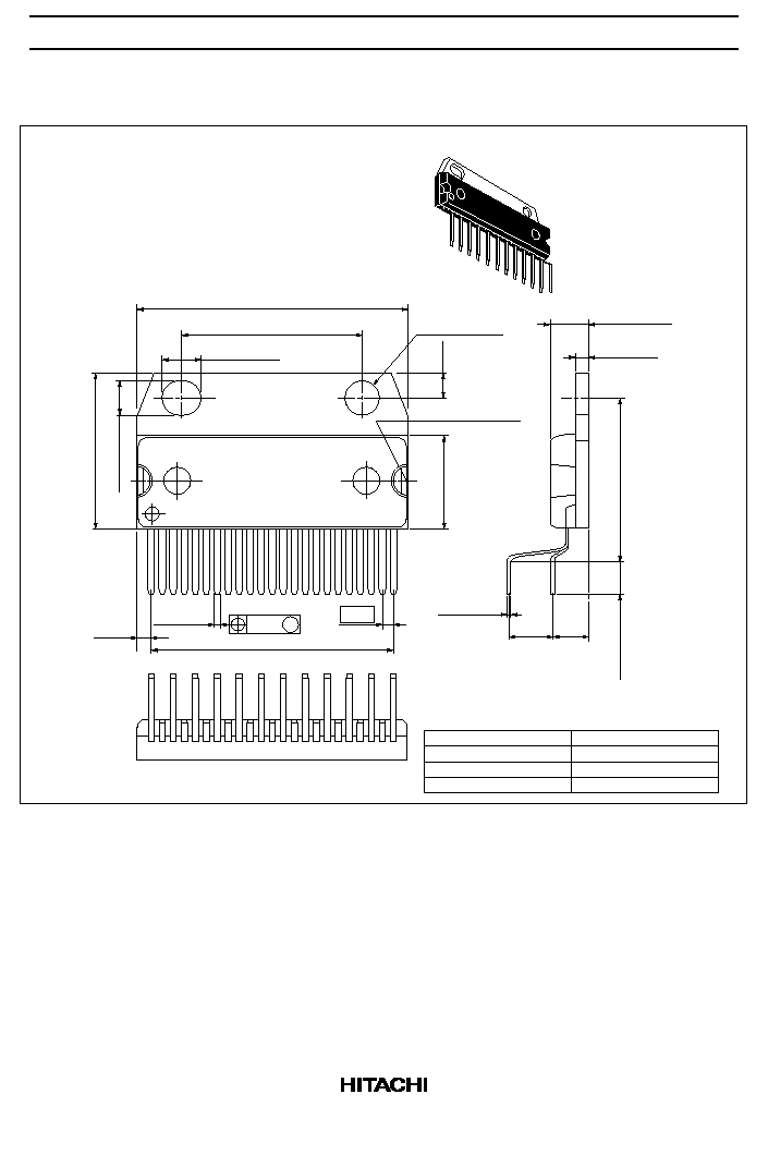
Package Dimensions
Hitachi Code
JEDEC
EIAJ
Weight (reference value)
SP-23TE
Conforms
--
8.5 g
Unit: mm
2 ≠ R1.84
±
0.19
4.32
±
0.05
19.81
30.18
±
0.25
2.79
10.70
±
0.12
3.80
±
0.05
+ 0.05
≠ 0.1
1.55
4.50
±
0.12
17.78
±
0.25
4.14
±
0.33
23
1
4.29
5.08
+ 0.06
≠ 0.04
0.40
3.80
±
0.05
17.50
±
0.13
0.70
+0.09
≠0.1
1.27
27.94
0.25 M
1.12

HA13153A, HA13154A
21
Cautions
1. Hitachi neither warrants nor grants licenses of any rights of Hitachi's or any third party's patent,
copyright, trademark, or other intellectual property rights for information contained in this document.
Hitachi bears no responsibility for problems that may arise with third party's rights, including
intellectual property rights, in connection with use of the information contained in this document.
2. Products and product specifications may be subject to change without notice. Confirm that you have
received the latest product standards or specifications before final design, purchase or use.
3. Hitachi makes every attempt to ensure that its products are of high quality and reliability. However,
contact Hitachi's sales office before using the product in an application that demands especially high
quality and reliability or where its failure or malfunction may directly threaten human life or cause risk
of bodily injury, such as aerospace, aeronautics, nuclear power, combustion control, transportation,
traffic, safety equipment or medical equipment for life support.
4. Design your application so that the product is used within the ranges guaranteed by Hitachi particularly
for maximum rating, operating supply voltage range, heat radiation characteristics, installation
conditions and other characteristics. Hitachi bears no responsibility for failure or damage when used
beyond the guaranteed ranges. Even within the guaranteed ranges, consider normally foreseeable
failure rates or failure modes in semiconductor devices and employ systemic measures such as fail-
safes, so that the equipment incorporating Hitachi product does not cause bodily injury, fire or other
consequential damage due to operation of the Hitachi product.
5. This product is not designed to be radiation resistant.
6. No one is permitted to reproduce or duplicate, in any form, the whole or part of this document without
written approval from Hitachi.
7. Contact Hitachi's sales office for any questions regarding this document or Hitachi semiconductor
products.
Hitachi, Ltd.
Semiconductor & Integrated Circuits.
Nippon Bldg., 2-6-2, Ohte-machi, Chiyoda-ku, Tokyo 100-0004, Japan
Tel: Tokyo (03) 3270-2111 Fax: (03) 3270-5109
Copyright ' Hitachi, Ltd., 1998. All rights reserved. Printed in Japan.
Hitachi Asia Pte. Ltd.
16 Collyer Quay #20-00
Hitachi Tower
Singapore 049318
Tel: 535-2100
Fax: 535-1533
URL
NorthAmerica
: http:semiconductor.hitachi.com/
Europe
: http://www.hitachi-eu.com/hel/ecg
Asia (Singapore)
: http://www.has.hitachi.com.sg/grp3/sicd/index.htm
Asia (Taiwan)
: http://www.hitachi.com.tw/E/Product/SICD_Frame.htm
Asia (HongKong)
: http://www.hitachi.com.hk/eng/bo/grp3/index.htm
Japan
: http://www.hitachi.co.jp/Sicd/indx.htm
Hitachi Asia Ltd.
Taipei Branch Office
3F, Hung Kuo Building. No.167,
Tun-Hwa North Road, Taipei (105)
Tel: <886> (2) 2718-3666
Fax: <886> (2) 2718-8180
Hitachi Asia (Hong Kong) Ltd.
Group III (Electronic Components)
7/F., North Tower, World Finance Centre,
Harbour City, Canton Road, Tsim Sha Tsui,
Kowloon, Hong Kong
Tel: <852> (2) 735 9218
Fax: <852> (2) 730 0281
Telex: 40815 HITEC HX
Hitachi Europe Ltd.
Electronic Components Group.
Whitebrook Park
Lower Cookham Road
Maidenhead
Berkshire SL6 8YA, United Kingdom
Tel: <44> (1628) 585000
Fax: <44> (1628) 778322
Hitachi Europe GmbH
Electronic components Group
Dornacher Stra
e 3
D-85622 Feldkirchen, Munich
Germany
Tel: <49> (89) 9 9180-0
Fax: <49> (89) 9 29 30 00
Hitachi Semiconductor
(America) Inc.
179 East Tasman Drive,
San Jose,CA 95134
Tel: <1> (408) 433-1990
Fax: <1>(408) 433-0223
For further information write to: