 | –≠–ª–µ–∫—Ç—Ä–æ–Ω–Ω—ã–π –∫–æ–º–ø–æ–Ω–µ–Ω—Ç: HA13164 | –°–∫–∞—á–∞—Ç—å:  PDF PDF  ZIP ZIP |

HA13164A
Multiple Voltage Regulator
ADE-207-342 (Z)
Rev.0
Jun. 2001
General Description
The HA13164A is a compact multiple voltage regulator for car audio system. The outputs of this IC output
consist of regulated 5.7 V output for a microcontroller, regulated 8 V output for CD driver, regulated 9.0 V
output for audio control, regulated 10 V output for illuminations and regulated 5 V output, VCC-dependent
output for external output and VCC-dependent output for remort-ANT.
Functions
General
∑
ACC power monitor circuit is built-in as to detect low voltage.
∑
Low saturation output (PNP output) used for audio output.
∑
Adjustable voltage for illumination output by changing an external resister.
Protections
∑
Output current limit circuit to avoid device destruction caused by shorted output, etc.
∑
High surge input protector against VCC and ACC.
∑
Built in a thermal shutdown circuit to prevent against the thermal destruction.
HA13164A
Rev.0, Jun. 2001, page 2 of 18
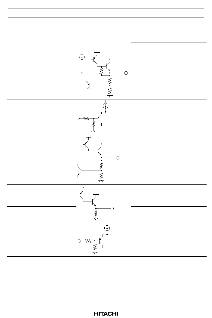
Pin Description and Equivalent Circuit
Function
Pin
No.
Pin Name
Specification
Equivalent Circuit
Normal Operation TSD
Surge Input
1
EXT OUT
VCC-1V/300mA min
Output voltage is
VCC-1 V when M
or H level applied to
CTRL pin.
0V
0V
2
ANT OUT
VCC-1V/300mA min
Vcc
90k
Vcc
10k
Output voltage is
VCC-1 V when M
or H level to CTRL
pin and H level to
ANT-CTRL.
0V
0V
3
ACCIN
--
15k
45k
Connected to ACC. --
--
4
VDD OUT
5.7V/100mA min
Vcc
175k
Vcc
50k
Regular 5.7V.
5.7V
0V
5
SW5VOUT
5.0V/100mA min
Output voltage is
5V when M or H
level applied to
CTRL pin.
0V
0V
6
COMPOUT
5.0V/100mA min
Vcc
50k
VDD
Output for ACC
detector
0V
0V
7
ANT CTRL
--
49k
51k
L: ANT output OFF
H: ANT output ON
--
--
HA13164A
Rev.0, Jun. 2001, page 3 of 18
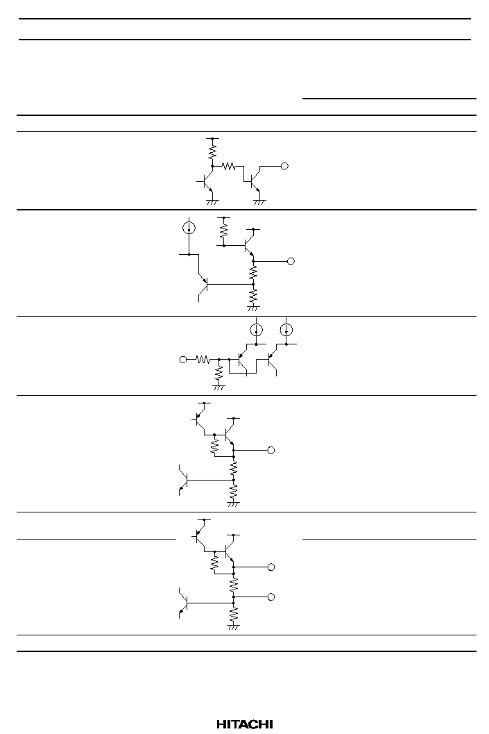
Pin Description and Equivalent Circuit (cont)
Function
Pin
No.
Pin Name
Specification
Equivalent Circuit
Normal Operation TSD
Surge Input
8
VCC
--
Connected to VCC
--
--
9
BATT DET
--
VDD
250k
10k
Low battery detect. Detect
Not detect
10
AUDIOOUT 9.0V/500mA min
Vcc
77.3k
Vcc
12.3k
Output voltage is
9V when M or H
level applied to
CTRL pin.
0V
0V
11
CTRL
--
35k
65k
L: BIAS OFF
M: BIAS ON
H: CD ON
--
--
12
CD OUT
8.0V/1.3A min
Vcc
64.7k
Vcc
12.4k
Output voltage is
8V when H level
applied to CTRL
pin.
0V
0V
13
ILM AJ
--
Adjustment pin for
ILM output voltage.
--
--
14
ILM OUT
9.85V/500mA min
Vcc
33.4k
Vcc
5k
Output voltage is
10V when M or H
level applied to
CTRL pin
0V
0V
15
GND
--
Connected to GND --
--
HA13164A
Rev.0, Jun. 2001, page 4 of 18
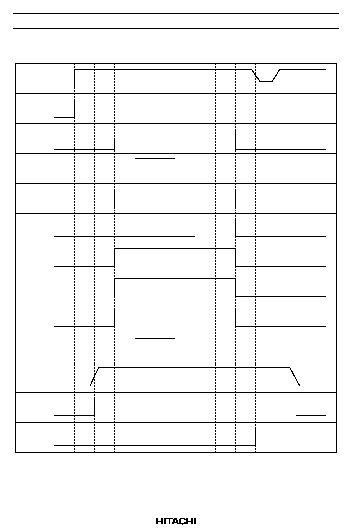
Timing Chart
VCC
VDD
CTRL
ANTCTRL
AUDIO
CD
ILM
EXT
SW5V
ANT
ACC
2.8V
2.5V
COMP
B.DET current
9.25V
8.5V
HA13164A
Rev.0, Jun. 2001, page 5 of 18
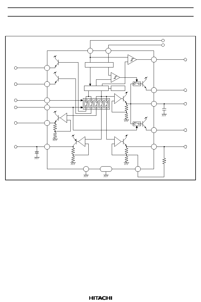
Block Diagram
-
+
-
+
-
+
2
ANT OUT
1
EXT OUT
ANT CTRL
7
11
CTRL
12
CC OUT
GND
ILM OUT
BIAS
TSD
-
+
10
14
AUDIO OUT
SW5V
5
VDD OUT
4
COMP OUT
6
BATT.DET
ACC
ACC
+B
9
8
VCC
3
+
TAB
GND
15
13
-
+
Surge protector
ILM AJ
-
+
HA13164A
Rev.0, Jun. 2001, page 6 of 18
Absolute Maximum Ratings
(Ta = 25
∞C)
Item
Symbol
Value
Unit
Note
Operating power supply voltage
Vcc
18
V
DC supply voltage
Vcc(DC)
26
V
1
Peak voltage
Vcc(PEAK)
50
V
2
Power dissipation
Pd
36
W
3
Junction temperature
Tj
150
∞C
Operating temperature
Topr
≠40 to +85
∞C
Storage temperature
Tstg
≠55 to +125
∞C
Notes: Recommended power supply voltage range 10V to 16V.
1. Applied time is less than 30 sec.
2. Surge pulse as input.
3. Ta=25∞C. :Permissible power dissipation when using a heat sink of infinite area. Refer to the
derating curves below.
Ambient temperature Ta (
∞
C)
0
50
100
75
25
1.8W
20
15
10
5
0
150
125
175
Power dissipation Pd (W)
8.7W
11.0W
w/o heat sink
thin = 1.6mm, 50cm
2
Aluminum heat sink
thin = 1.6mm, 100cm
2
Aluminum heat sink
HA13164A
Rev.0, Jun. 2001, page 7 of 18
Electrical Characteristics
(unless otherwise noted, Vcc = 13.2 V, Ta = 25∞C)
Item
Symbol Min
Typ
Max
Unit Test Condition
Standby current
IST
--
460
700
µ
A
ACC = 0V, CTRL = 0V
CTRL L level (STBY mode)
VCL
0
--
1.0
V
CTRL M level (CD OFF mode)
VCM
2.0
--
3.0
V
CTRL H level (CD ON mode)
VCH
4.0
--
--
V
ANT CTRL L level (ANTOFF mode)
VACL
0
--
2.0
V
ANT CTRL H level (ANT ON mode)
VACH
3.0
--
--
V
Output voltage
Vo1
5.4
5.7
6.0
V
Io1 = 80mA
Voltage regulation
Vo11
--
10
50
mV
Vcc = 10 to 16V, Io1 = 80mA
Load regulation
Vo12
--
50
100
mV
Io1 = 0 to 80mA
Minimum I/O voltage differential
Vo13
--
1.0
1.5
V
Io1 = 80mA
Output current capacity
Io1
100
250
--
mA
Vo1
5.4V
VDD
OUT
Ripple rejection ratio
SVR1
50
60
--
dB
f = 100Hz, Io1 = 80mA
Output voltage 2
Vo2
7.6
8.0
8.4
V
Io2 = 1.0A
Voltage regulation
Vo21
--
40
100
mV
Vcc = 10 to 16V, Io2 = 1.0A
Load regulation
Vo22
--
70
150
mV
Io2 = 10m to 1.0A
Minimum I/O voltage differential
Vo23
--
1.0
1.5
V
Io2 = 1.0A
Output current capacity
Io2
1.3
2.0
--
A
Vo2
7.6V
CD
OUT
Ripple rejection ratio
SVR2
40
45
--
dB
f = 100Hz, Io2 = 1.0A
Output voltage 3
Vo3
8.5
9.0
9.5
V
Io3 = 400mA
Voltage regulation
Vo31
--
30
90
mV
Vcc = 10 to 16V, Io3 = 400mA
Load regulation
Vo32
--
100
200
mV
Io3 = 10 to 400mA
Minimum I/O voltage differential
Vo33
--
0.4
0.9
V
Io3 = 400mA
Output current capacity
Io3
500
850
--
mA
Vo3
8.5V
AUDIO
OUT
Ripple rejection ratio
SVR3
45
50
--
dB
f = 100Hz, Io3 = 400mA
Output voltage 4
Vo4
9.35
9.85
10.35
V
Io4 = 400mA
Voltage regulation
Vo41
--
40
100
mV
Vcc = 12.5 to 16V, Io4 = 400mA
Load regulation
Vo42
--
50
100
mV
Io4 = 10 to 400mA
Minimum I/O voltage differential
Vo43
--
1.0
1.5
V
Io4 = 400mA
Output current capacity
Io4
500
900
--
mA
Vo4
9.35V
ILM
OUT
Ripple rejection ratio
SVR4
35
40
--
dB
f = 100Hz, Io4 = 400mA
Differential I/O voltage
Vo51
--
1.0
1.5
V
Io5 = 300mA
Load regulation
Vo52
--
350
600
mV
Io5 = 10 to 300mA
EXT12
OUT
Output current capacity
Io5
300
500
--
mA
Vo5
11.7V
HA13164A
Rev.0, Jun. 2001, page 8 of 18
Electrical Characteristics (cont)
(unless otherwise noted, Vcc = 13.2 V, Ta = 25∞C)
Item
Symbol Min
Typ
Max
Unit Test Condition
Differential I/O voltage
Vo61
--
1.0
1.5
V
Io6 = 300mA
Load regulation
Vo62
--
350
600
mV
Io6 = 10 to 300mA
ANT
OUT
Output current capacity
Io6
300
500
--
mA
Vo6
11.7V
Output voltage
Vo7
4.6
5.0
5.4
V
Io7 = 80mA, VDD = no load
SW5V
OUT
Output current capacity
Io7
100
300
--
mA
Vo7
4.6V
Output voltage
Vo8
4.6
5.0
5.4
V
Io8 = 40mA, VDD = no load
Output current capacity
Io8
100
300
--
mA
Vo8
4.6V
Rise threshold voltage
VTHH8
2.6
2.8
3.0
V
ACC
OUT
Hysteresis range
VTH8
0.2
0.3
0.4
V
Threshold voltage
VTHH9
8.1
8.5
8.9
V
Hysteresis range
VTH9
0.55
0.75
0.95
V
BATT.
DET
Output current capacity
Io9
200
--
--
µ
A
Vo = 0.3V

HA13164A
Rev.0, Jun. 2001, page 9 of 18
Evaluation Circuit
1
EXT
HA13164
2
ANT
3
ACC
4
VDD
5
SW5V
6
COMP
7
ANT CTRL
8
VCC
9
BATT.DET
10
AUDIO
11
CTRL
12
CD
13
ILM.AJ
14
ILM
15
GND
EXT
ANT
ACC
VDD
SW5V
COMP
ANT CTRL VCC
BATT.DET AUDIO
CTRL
CD
ILM
SW1
SW2 SW3
SW4
C7
0.1
µ
F
R2
3.3k
C6
100
µ
F
C1
0.1
µ
F
C2
0.1
µ
F
C3
0.1
µ
F
C8
10
µ
F
C9
0.1
µ
F
C10
0.1
µ
F
5V
+
+
R3
3.3k
HA13164A
Rev.0, Jun. 2001, page 10 of 18
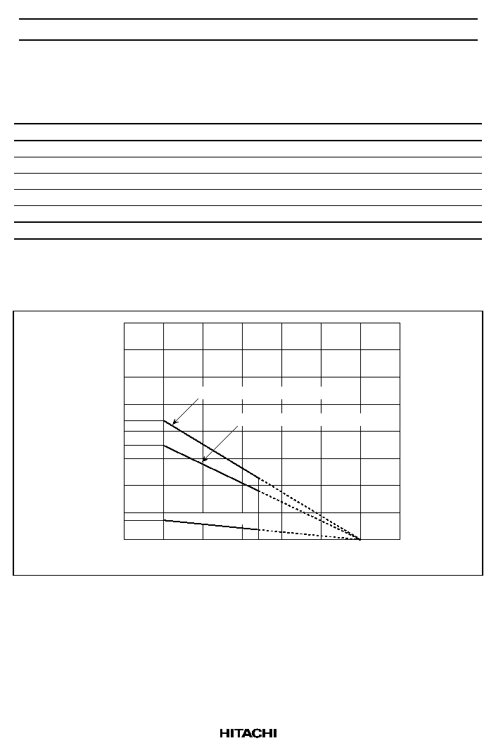
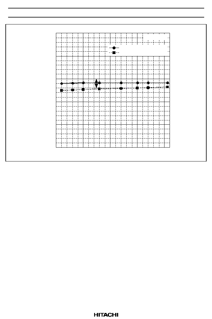
Main Characteristic
0
1
2
3
4
5
6
≠50
0
50
100
150
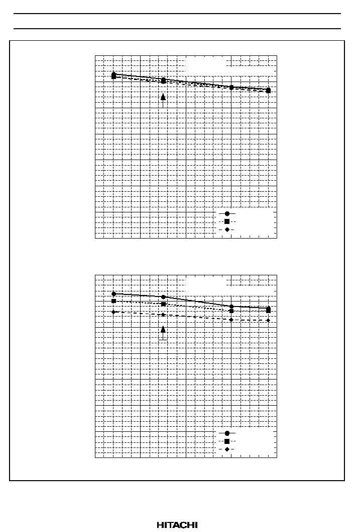
CTRL, ANTCTRL Vth vs. Tc
CTRL, ANTCTRL voltage (V)
Tc (
∞
C)
CTRL 'L/M' Vth (1.0V
Vth
2.0V)
ANTCTRL Vth (2.0V
Vth
3.0V)
CTRL 'M/H' Vth (3.0V
Vth
4.0V)
Vcc = 13.2V
B.DET Detection vs. Tc
Vth (0.55V
Vth
0.95V)
Vth (8.1V
Vth
8.9V)
≠50
0
50
100
150
Tc (
∞
C)
7
7.5
8
8.5
9
9.5
10
10.5
11
VCC voltage (V)
HA13164A
Rev.0, Jun. 2001, page 11 of 18
0
1
2
3
4
5
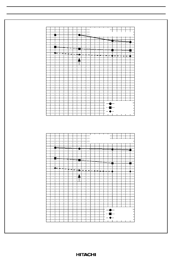
ACC Detection vs. Tc
≠50
0
50
100
150
Tc (
∞
C)
ACC voltage (V)
Vcc = 13.2V
Vth (2.6V
Vth
3.0V)
Vth (0.2V
Vth
0.4V)
HA13164A
Rev.0, Jun. 2001, page 12 of 18
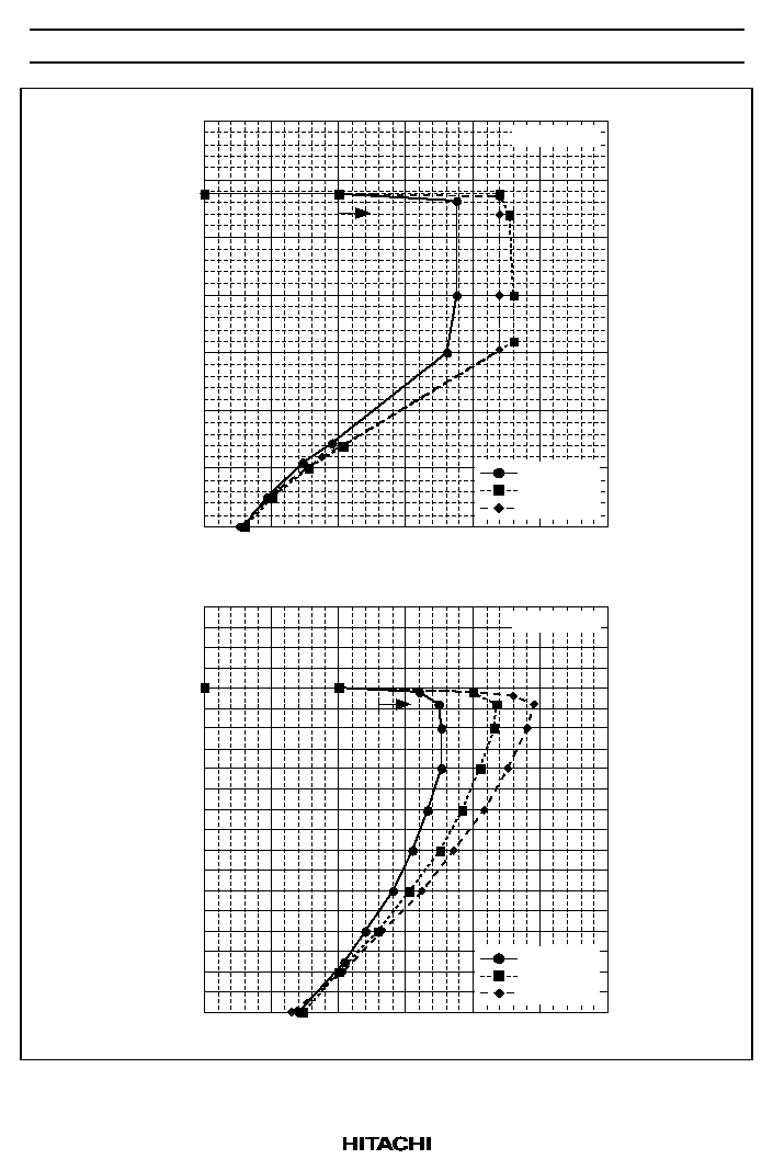
0
1
2
3
4
5
6
7
300
0
50
100
150
200
250
Io (mA)
Tc = 100
∞
C
Tc = 25
∞
C
Tc = ≠30
∞
C
Vcc = 13.2V
Vo ≠ Io Characteristics VDD Output
VDD output voltage (V)
0
2
4
6
8
10
0
0.5
1
1.5
2
2.5
3
Io (A)
Tc = 100
∞
C
Tc = 25
∞
C
Tc = ≠30
∞
C
Vcc = 13.2V
Vo ≠ Io Characteristics CD Output
CD output voltage (V)
HA13164A
Rev.0, Jun. 2001, page 13 of 18
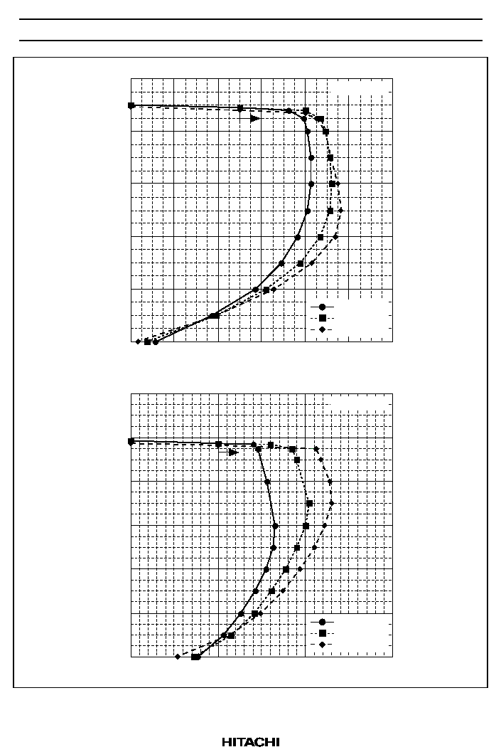
0
2
4
6
8
10
0
200
400
600
800
1000
1200
Io (mA)
Tc = 100
∞
C
Tc = 25
∞
C
Tc = ≠30
∞
C
Vcc = 13.2V
Vo ≠ Io Characteristics AUDIO output
AUDIO output voltage (V)
0
2
4
6
8
10
12
0
500
1000
1500
Io (mA)
Tc = 100
∞
C
Tc = 25
∞
C
Tc = ≠30
∞
C
Vcc = 13.2V
Vo ≠ Io Characteristics ILM output
ILM output voltage (V)
HA13164A
Rev.0, Jun. 2001, page 14 of 18
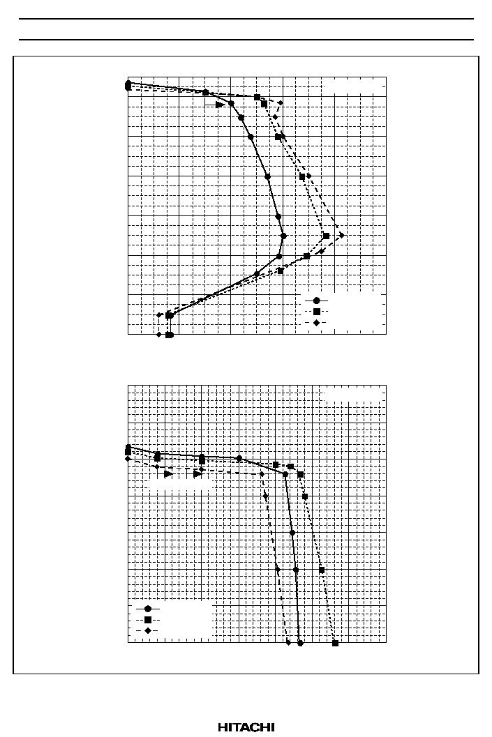
0
2
4
6
8
10
12
0
200
400
600
800
1000
Io (mA)
Tc = 100
∞
C
Tc = 25
∞
C
Tc = ≠30
∞
C
Vcc = 13.2V
Vo ≠ Io Characteristics EXT, ANT Output
EXT output voltage (V)
0
1
2
3
4
5
6
7
0
50
100
150
200
250
300
350
Io (mA)
Tc = 100
∞
C
Tc = 25
∞
C
Tc = ≠30
∞
C
Vcc = 13.2V
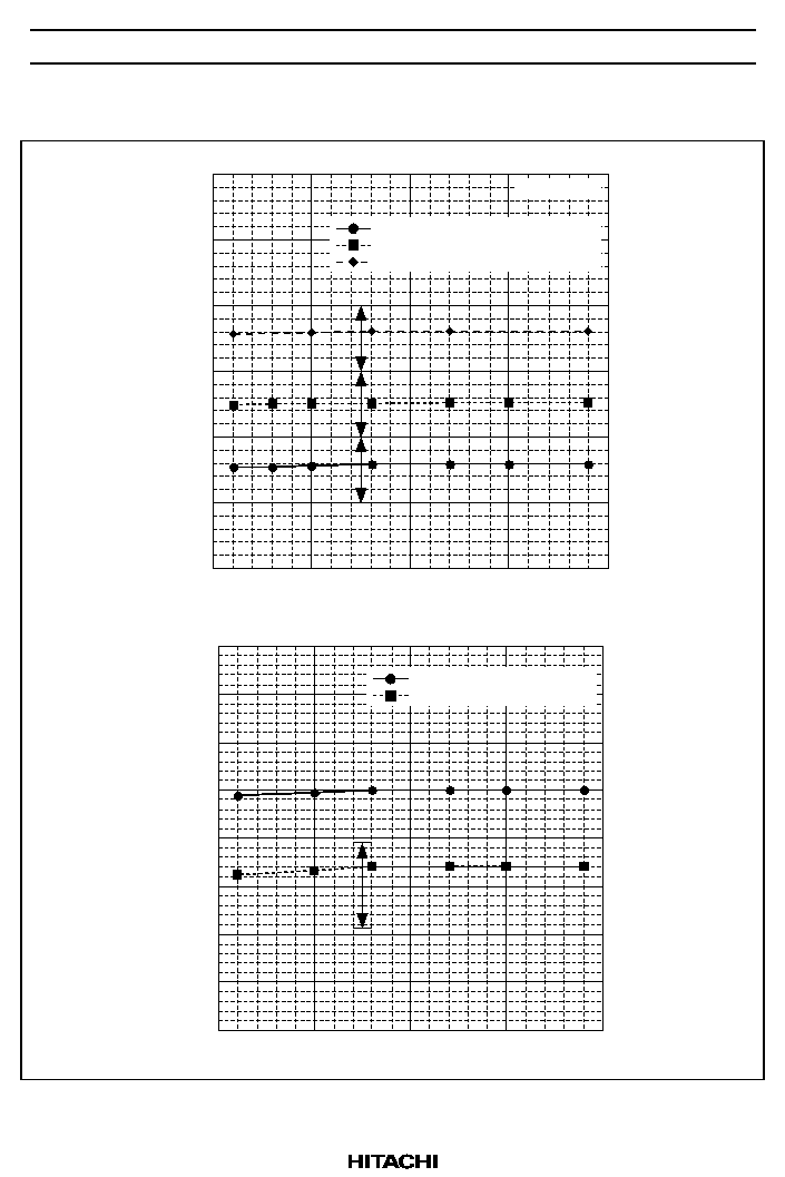
Vo ≠ Io Characteristics COMP, SW5V Output
COMP, SW5V output voltage (V)
COMP SW5V
HA13164A
Rev.0, Jun. 2001, page 15 of 18
≠50
0
50
100
150
SVR vs. Tc VDD Output
0
10
20
30
40
50
60
70
SVR (dB)
Tc (
∞
C)
Vcc = 13.2V
Ripple f = 100Hz, v = 0dBm
Io = 10mA
Io = 40mA
Io = 80mA
0
10
20
30
40
50
60
70
SVR vs. Tc CD Output
SVR (dB)
≠50
0
50
100
150
Tc (
∞
C)
Vcc = 13.2V
Ripple f = 100Hz, v = 0dBm
Io = 10mA
Io = 500mA
Io = 1A
HA13164A
Rev.0, Jun. 2001, page 16 of 18
0
10
20
30
40
50
60
70
SVR vs. Tc AUDIO Output
SVR (dB)
≠50
0
50
100
150
Tc (
∞
C)
Vcc = 13.2V
Ripple f = 100Hz, v = 0dBm
Io = 10mA
Io = 200mA
Io = 400mA
0
10
20
30
40
50
60
70
SVR vs. Tc ILM Output
SVR (dB)
≠50
0
50
100
150
Tc (
∞
C)
Vcc = 13.2V
Ripple f = 100Hz, v = 0dBm
Io = 10mA
Io = 200mA
Io = 400mA
HA13164A
Rev.0, Jun. 2001, page 17 of 18
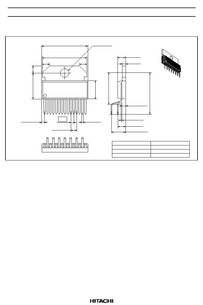
Package Dimensions
Hitachi Code
JEDEC
EIAJ
Mass (reference value)
SP-15TA
--
--
3.10 g
11.3
± 0.3
3.0 ± 0.2
7.8
19.66
19.0 ± 0.3
0.6 ± 0.1
1.27
1.11 ± 0.25
3.8 Max
1.5 Max
1.80 ± 0.25
6.04 ± 0.50
3.5 ± 0.5
17.90
13.8
0.25
+ 0.10
≠ 0.05
3.6 ± 0.2
1
15
3.0 ± 0.2
3.0 ± 0.2
20.5 Max
2.54±0.25
Unit: mm
HA13164A
Rev.0, Jun. 2001, page 18 of 18
Disclaimer
1. Hitachi neither warrants nor grants licenses of any rights of Hitachi's or any third party's patent,
copyright, trademark, or other intellectual property rights for information contained in this document.
Hitachi bears no responsibility for problems that may arise with third party's rights, including
intellectual property rights, in connection with use of the information contained in this document.
2. Products and product specifications may be subject to change without notice. Confirm that you have
received the latest product standards or specifications before final design, purchase or use.
3. Hitachi makes every attempt to ensure that its products are of high quality and reliability. However,
contact Hitachi's sales office before using the product in an application that demands especially high
quality and reliability or where its failure or malfunction may directly threaten human life or cause risk
of bodily injury, such as aerospace, aeronautics, nuclear power, combustion control, transportation,
traffic, safety equipment or medical equipment for life support.
4. Design your application so that the product is used within the ranges guaranteed by Hitachi particularly
for maximum rating, operating supply voltage range, heat radiation characteristics, installation
conditions and other characteristics. Hitachi bears no responsibility for failure or damage when used
beyond the guaranteed ranges. Even within the guaranteed ranges, consider normally foreseeable
failure rates or failure modes in semiconductor devices and employ systemic measures such as fail-
safes, so that the equipment incorporating Hitachi product does not cause bodily injury, fire or other
consequential damage due to operation of the Hitachi product.
5. This product is not designed to be radiation resistant.
6. No one is permitted to reproduce or duplicate, in any form, the whole or part of this document without
written approval from Hitachi.
7. Contact Hitachi's sales office for any questions regarding this document or Hitachi semiconductor
products.
Sales Offices
Hitachi, Ltd.
Semiconductor & Integrated Circuits.
Nippon Bldg., 2-6-2, Ohte-machi, Chiyoda-ku, Tokyo 100-0004, Japan
Tel: Tokyo (03) 3270-2111 Fax: (03) 3270-5109
Copyright
Hitachi, Ltd., 2000. All rights reserved. Printed in Japan.
Hitachi Asia Ltd.
Hitachi Tower
16 Collyer Quay #20-00,
Singapore 049318
Tel : <65>-538-6533/538-8577
Fax : <65>-538-6933/538-3877
URL : http://www.hitachi.com.sg
URL
NorthAmerica
: http://semiconductor.hitachi.com/
Europe
: http://www.hitachi-eu.com/hel/ecg
Asia
: http://sicapac.hitachi-asia.com
Japan
: http://www.hitachi.co.jp/Sicd/indx.htm
Hitachi Asia Ltd.
(Taipei Branch Office)
4/F, No. 167, Tun Hwa North Road,
Hung-Kuo Building,
Taipei (105), Taiwan
Tel : <886>-(2)-2718-3666
Fax : <886>-(2)-2718-8180
Telex : 23222 HAS-TP
URL : http://www.hitachi.com.tw
Hitachi Asia (Hong Kong) Ltd.
Group III (Electronic Components)
7/F., North Tower,
World Finance Centre,
Harbour City, Canton Road
Tsim Sha Tsui, Kowloon,
Hong Kong
Tel : <852>-(2)-735-9218
Fax : <852>-(2)-730-0281
URL : http://www.hitachi.com.hk
Hitachi Europe Ltd.
Electronic Components Group.
Whitebrook Park
Lower Cookham Road
Maidenhead
Berkshire SL6 8YA, United Kingdom
Tel: <44> (1628) 585000
Fax: <44> (1628) 585160
Hitachi Europe GmbH
Electronic Components Group
Dornacher Straþe 3
D-85622 Feldkirchen, Munich
Germany
Tel: <49> (89) 9 9180-0
Fax: <49> (89) 9 29 30 00
Hitachi Semiconductor
(America) Inc.
179 East Tasman Drive,
San Jose,CA 95134
Tel: <1> (408) 433-1990
Fax: <1>(408) 433-0223
For further information write to:
Colophon 2.0