 | –≠–ª–µ–∫—Ç—Ä–æ–Ω–Ω—ã–π –∫–æ–º–ø–æ–Ω–µ–Ω—Ç: HA13536F | –°–∫–∞—á–∞—Ç—å:  PDF PDF  ZIP ZIP |

HA13536F
Three-Phase Brushless DC Motor Driver IC
ADE-207-111B (Z)
3rd Edition
July 1996
Description
The HA13536F is a 3-phase brushless DC motor driver IC with digital speed control. It is being developed
for direct drive of the spindle motor of 5 V floppy disk drives with a height of 3/4" or less. It has the follow-
ing functions and features.
Functions
∑
1.0 A per phase, 3-phase drive circuit (current driver)
∑
Digital speed control circuit
∑
FG Amp
∑
Index circuit
∑
Current limiter circuit
∑
Over-temperature shutdown circuit (OTSD)
Features
∑
Low saturation voltage, typically 1.15 V (at 0.7 A)
∑
Soft switching drive circuit
∑
No need for an output snubber circuit

HA13536F
2
Pin Arrangement
25
26
27
28
1 2 3
TAB
4
5 6
10
9
8
7
14
13
12
11
TAB
20 19
TAB
17 16 15
21
22
23
24
TAB
V phase + input
V phase ≠ input
W phase + input
W phase ≠ input
AGC
Index + input
Index ≠ input
FG + input
Bias output
U phase output
V phase output
Current detection
W phase output
Phase compensation
Charge pump output
CLK input
FG ≠ input
RPM SEL
Index adjust
Index Vreg
Index output
CE
U phase ≠ input
U phase + input
V
CC
Hall bias
Bias ≠ pin
Bias + pin
18
(Top view)
HA13536F
3
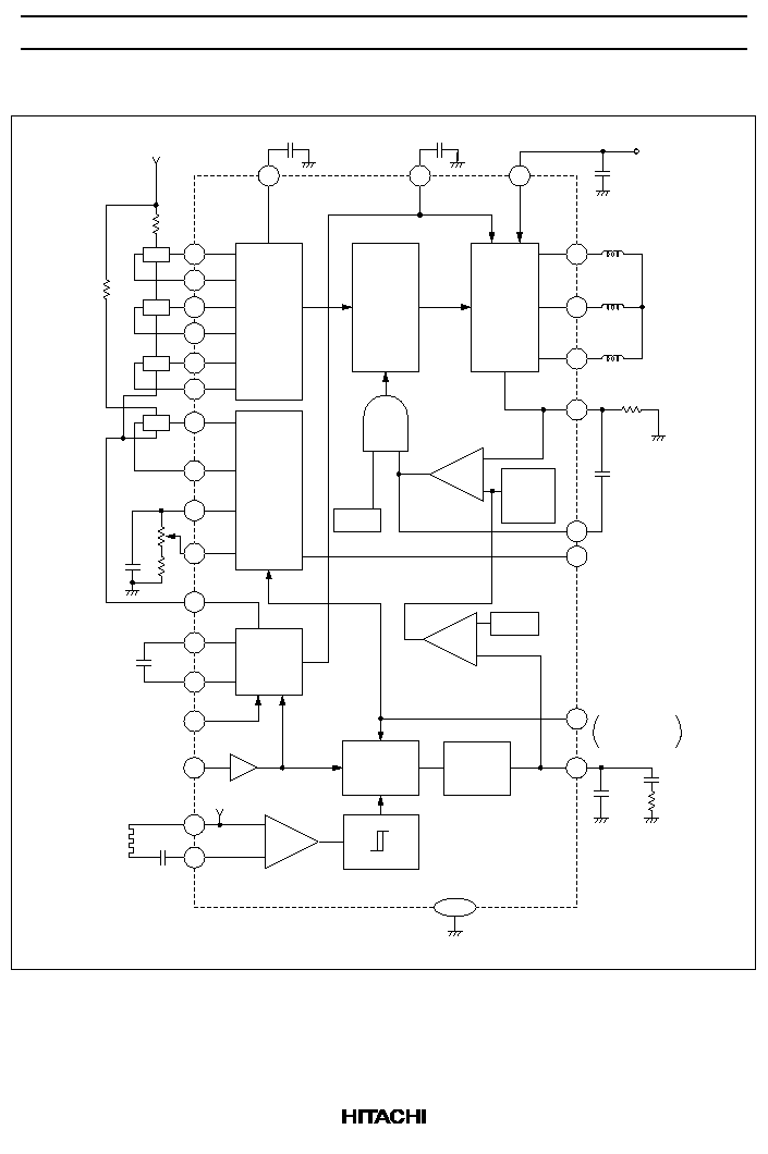
Block Diagram
25
14
18
13
12
10
11
9
8
1
28
7
6
15
16
17
4
3
27
26
23
21
19
Hall
Amp
Matrix
Output
Amp
Hu
Index
circuit
Bias
Vref2
Charge
pump
R101
V
CC
C102
C105
V
5 V
CC
C101
Rnf
Index output
(Open collector)
C1
C2
Rt1
Ct
R2
C104
CE
CLK
1 MHz
FG
60 ppr
FG Amp.
RPM select
H: 360 rpm
L: 300 rpm
u (+)
v (+)
w (+)
U
V
W
TAB
C103
Buffer Amp.
2
5
OTSD
Current
limitter
Vref1
Control Amp.
C106
≠
+
≠
+
Speed
discrim-
inator
+
≠
24
22
20
Hv
Hw
Hi
R102
1.6 V
u (-)
v (-)
w (-)
(+)
(-)
Rt2
Note : Pin arrangement is preliminary specification.

HA13536F
4
Pin Function
Pin Number Pin Name
Function
Pin Voltage
1
FG (≠) input
FG Amp. (≠) input terminal
2
RPMSEL
Change terminal for motor rotation speed
"L"
300 rpm, "H"
360 rpm
V
TH
= 1.4 V Typ
3
Index adjustment
Terminal to set up burst time of index circuit
0 V Min, 1.2 V Max
4
Index Vreg
Output terminal for fixed voltage of index circuit
1.5 V Typ
5
Index output
Index output terminal (Open collector)
V
OL
= 0.14 V Typ
(@I
O
= 2 mA)
6
CE
Chip enable terminal
"L": enable, "H": disable
V
TH
= 1.4 V Typ
7
CLK input
CLK input terminal
V
TH
= 1.4 V Typ
8
C-PUMP output
Speed error Integration and Phase compensation of
speed control
9
Phase compensation To prevent the parastic oscillation of output, insert
the capacitor between pin 9 and pin 11.
10
W phase output
W phase output
11
Current detection
Output current detection and terminal which is con-
nected with phase compensation capacitor for car-
rent control.
12
V phase output
V phase output
13
U phase output
U phase output
14
Bias output
Bias output terminal
15
Bias (+) pin
Bias (+) pin terminal
16
Bias (≠) pin
Bias (≠) pin terminal
17
Hall bias
Hall bias terminal
CE
= "L"
Bias,
CE
= "H"
High impedance
2.2 V Typ
(@I = 10 mA)
18
V
CC
Power supply
4.25 V Min, 6.5 V
Max
19
U phase (+) input
U phase (+) input terminal
2.0 V Min,
V
CC
≠ 0.5 V Max
20
U phase (≠) input
U phase (≠) input terminal
2.0 V Min,
V
CC
≠ 0.5 V Max
21
V phase (+) input
V phase (+) input terminal
2.0 V Min,
V
CC
≠ 0.5 V Max
22
V phase (≠) input
V phase (≠) input terminal
2.0 V Min,
V
CC
≠ 0.5 V Max
23
W phase (+) input
W phase (+) input terminal
2.0 V Min,
V
CC
≠ 0.5 V Max
24
W phase (≠) input
W phase (≠) input terminal
2.0 V Min,
V
CC
≠ 0.5 V Max
25
AGC
Hall amp output wave form adjustment terminal
(Insert capacitor C102 between GND)

HA13536F
5
Pin Function (cont)
Pin Number Pin Name
Function
Pin Voltage
26
Index (+) input
Index amp (+) input terminal
1.4 V Min,
V
CC
≠ 0.5 V Max
27
Index (≠) input
Index amp (≠) input terminal
1.4 V Min,
V
CC
≠ 0.5 V Max
28
FG (+) input
FG amp (+) input terminal
DC bias 1.6 V Typ
External Parts
Part Number
Recommended Value
Purpose
Notes
R2
--
Integration constant
1
R101
--
Hall bias
R102
--
Index hall bias
Rnf
--
Current detection and limitation
2
Rt1
0 to 50 k
Index burst adjustment
3
Rt2
100 k
Index pulse width setting
C1, C2
--
Integration constants
1
C101
0.1
µ
F
Power supply bypass
4
C102
0.1
µ
F
AGC filter
5
C103
0.47
µ
F
FG amp. coupling
5
C104
0.1
µ
F
Bias
C105
0.1
µ
F
Bias
7
C106
0.1
µ
F
Phase compensation
4
Ct
0.1
µ
F
Index setting
3, 6
Notes: 1. Determine the integration constants from the following formulas:
O
2
f
FG
20
R2 =
1
9.55
J
O
N
K
T
Gctl Icp
C1 =
1
10
1
O
R2
C2 = 10C1
(rad/s)
(
)
(F)
(F)
O
Rnf
.

HA13536F
6
In the above formulas:
O
= Time constant of servo loop
f
FG
= FG frequency in Hz
N
O
= Motor speed in rpm
J
= Motor moment of inertia in kg∑cm∑s
2
K
T
= Motor torque constant in kg∑cm/A
Rnf = Current detection in
Gctl = Control amp gain (see Electrical Characteristics)
Icp = Charge pump output current (see Electrical Characteristics)
2. The current limiter operates according to the following formula:
Vref1
Rnf
I
OMAX =
(A)
where Vref1 is the current limiter reference voltage (see Electrical Characteristics)
3. The burst time t1 is defined as follows:
t1
≠ Ct
◊
Rt1'
◊
ln (1 ≠ Vth1 (L) / Vreg) (RPM select input low)
t1
≠ Ct
◊
Rt1'
◊
ln (1 ≠ Vth1 (H) / Vreg) (RPM select input high)
where Rt1' is resistance value inter 3 to 4 pin.
4. Place as close to the IC as possible.
5. Determine C102 and C103 according to the following formulas:
C102 >
200
N P
(
µ
F)
C103 >
100
f
FG
(
µ
F)
O
where
P = Number of motor poles
6. The index pulse width t2 is determined as follows:
t2
≠ Ct
◊
Rt2'
◊
ln (Vth1 / Vth2)
where Vth2 is the threshold voltage (see Electrical Characteristics).
Rt2' : Rt1 (max) + Rt2
7. If the circuit is affected by noise, a large capacitance value should be set.
HA13536F
7
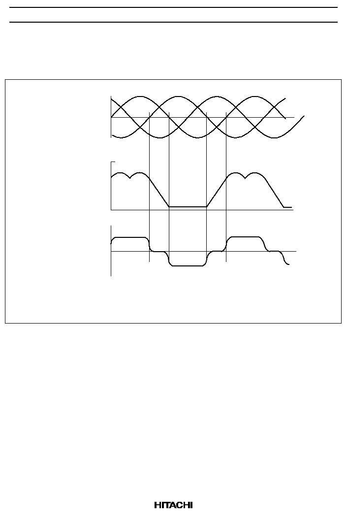
Timing Waveforms
Hall Amp Input vs. Output Voltage and Current
+
0
≠
U
V
W
Hall amp input
Output current
V
CC
0
U
+
0
≠
U
Output voltage
Notes: 1.
2.
The input waveforms to the hall amp should be sine waves with a third
harmonic content of less than 20%.
Only the U phase output is shown.
*
2
*
1
*
2
HA13536F
8
Index Amp Input vs. Output
∑
Application 1
20 to 100 mV
20 to 100 mV
t1
t2
+
0
≠
0
CC
Index amp input
Index output
V
Vth1
Vth2
Pin 3 voltage
0
∑
Application 2
20 to 100 mV
20 to 100 mV
t1
t2
+
0
≠
0
CC
Index amp
differential input
Index output
V
Vth1
Vth2
Pin 3 voltage
0

HA13536F
9
Absolute Maximum Ratings (Ta = 25
∞
C)
Item
Symbol
Value
Unit
Notes
Power supply voltage
V
CC
7
V
1
Input voltage
Vin
0 to V
CC
+ 0.3
V
2
Peak output current
I
OP
1.0
A
Normal output current
I
O
0.7
A
Power dissipation
P
T
1.5
W
3
Junction temperature
Tj
+150
∞
C
1
Storage temperature range
Tstg
≠55 to +125
∞
C
Notes: 1. The operating ranges is:
V
CC
= 4.25 to 6.5 V
Tjopr = 0 to +125
∞
C
2. Applied to the
CE
, CLK, and RPM SEL pins.
3. Permissible value when Tpin = 113
∞
C and thermal resistance is as follows:
j≠pin
25
∞
C/W
j≠a1
55
∞
C/W (when mounted on a metal substrade)
j≠a2
80
∞
C/W (when mounted on a glass epoxy substrade)

HA13536F
10
Electrical Characteristics (Ta = 25
∞
C, V
CC
= 5 V)
Item
Symbol
Min
Typ
Max
Unit
Test condi-
tions
Pin
Nos.
Notes
Quiscent
current
I
CCO
--
--
0.45
mA
CE
= H, V
CC
=
6.5 V
18
I
CC
--
9
13
mA
CE
= L, V
CC
=
6.5 V
Logic input Input current
(6 pin)
I
I1
≠80
--
2
µ
A
VCE
= 0 to 6.5
V
2, 6, 7
Input current
(2 pin)
I
I2
≠2
--
100
µ
A
V
RPM
= 5.5 V
Input current
(7 pin)
I
I3
≠2
--
450
µ
A
V
CLK
= 5.5 V
Input low
voltage
V
IL
0
--
0.8
V
Input high
voltage
V
IH
2.0
--
5.5
V
Logic out-
put
Output low
voltage
V
OL
--
--
0.4
V
I
O
= 2 mA
5
Leakage
current
I
OH
--
--
±
10
µ
A
V
CE
= 7.0 V
Hall amp
Input
resistance
Rhi
7
10
13
k
19 to 24
Common-
mode input
voltage
range
V
H
2.0
--
V
CC
≠ 0.5 V
Differential
input volt-
age range
Vh
30
--
160
mV
PP
Output
amp
Leakage
current
I
CER(H)
0
--
5
mA
V
O
= 7.0 V
10, 12,
13
I
CER(L)
--
--
±
100
µ
A
V
O
= 0 V
Saturation
voltage
Vsat1
--
1.15
1.65
V
I
O
= 0.7 A
1
Vsat2
--
0.6
0.85
V
I
O
= 0.35 A
FG amp
and de-
tector
Input
voltage
range
Vfg
2
--
20
mV
PP
1, 28
Noise
margin
nd
--
--
0.5
mV
PP
Differential
Noise
nc
--
--
0.5
V
COMMON
Noise

HA13536F
11
Electrical Characteristics (Ta = 25
∞
C, V
CC
= 5 V) (cont)
Item
Symbol
Min
Typ
Max
Unit
Test condi-
tions
Pin
Nos.
Notes
Speed
discrimi-
nator and
charge
pump
Number of
counts
N
--
1666.5
--
--
PRMSEL = L
--
1388.5
--
--
PRMSEL = H
Operating
frequency
f
CLK
0.9
1.0
1.1
MHz
7
Leakage
current
Ioff
--
--
±
50
nA
V8 = 0.8 V
8
Output
current
Icp+
7
10
13
µ
A
Speed reduc-
tion full scale
Icp≠
≠7
≠10
≠13
µ
A
Acceleration
full scale
Current
control
Threshold
voltage
Vref2
0.55
0.63
0.71
V
8
2
Voltage gain Gctl
≠12
≠10
≠8
dB
11
Current
limitter
voltage
Vref1
157
175
193
mV
R
NF
= 0.47
Index cir-
cuit
Input
voltage
(common)
Vindex
1.4
--
V
CC
≠ 0.5 V
26, 27
3
Input
voltage
(different)
Vindex
40
--
300
mVpp
Hysteresis
hys
--
14
--
mV
Input current
--
--
±
2
µ
A
3
Threshold
voltage
Vth1
0.60
◊
Vreg
0.64
◊
Vreg
0.68
◊
Vreg
V
RPM select = L
0.54
◊
Vreg
0.58
◊
Vreg
0.62
◊
Vreg
V
RPM select = H
Ct discharge
threshold
voltage
Vth2
0.50
◊
Vreg
0.54
◊
Vreg
0.58
◊
Vreg
V
RPMSEL = L
3
3
0.44
◊
Vreg
0.48
◊
Vreg
0.52
◊
Vreg
V
RPMSEL = H
Bias
Vreg
1.3
1.5
1.7
V
I
O
= ≠0.2 mA
4
Hall bias
Output
voltage
Vhb
1.9
2.2
2.5
V
Ih = 10 mA,
CE
= L
17

HA13536F
12
Electrical Characteristics (Ta = 25
∞
C, V
CC
= 5 V) (cont)
Item
Symbol
Min
Typ
Max
Unit
Test condi-
tions
Pin
Nos.
Notes
Hall bias
Leakage
current
Ihof
--
--
±
10
µ
A
CE
= H, Vhb =
7.0 V
17
OTSD
Operating
temperature
Tsd
125
150
--
∞
C
4
Notes: 1. Total of sink and source.
2. See figure 1. Gctl =
Vrnf/
Vcp.
3. Refer to the timing chart.
4. Design parameter only (No test).
Vrnf
Vcp
Vcp (8 pin)
Vrnf (Pin 11)
0
Vref2
Vref1
Figure 1

HA13536F
13
Reference Data
20
15
10
5
0
2
4
6
1.00
0.75
0.50
0.25
8
Power supply voltage V
CC
(V)
Quiscent current I
CC
(mA)
Quiscent current I
CCO
(mA)
I
CC
I
CCO
190
180
170
160
0.2
0.4
0.6
Current limitter voltage Vref1 (mV)
1.0
V
CC
= 5 V
150
0.8
R
NF
(
)
2.0
1.5
1.0
0.5
0
0.5
1.0
Output current I
O
(A)
Output saturation voltage Vsat (V)
1.5
V
CC
= 5 V
source
sink
sink + source
20
15
10
5
0
1
2
3
4
Hall bias voltage Vhb (V)
Hall bias current Ih (mA)
V
CC
= 5 V

HA13536F
14
Mount Waveform Characteristics
Time (20 ms / div)
0V
0V
0V
0V
Hall input (+)
(50 mV / div)
Output
(1 V / div)
Charge pump output
(0.5 V / div)
Phase compensation
(0.5 V / div)
Time (2 ms / div)
0V
0V
0V
0V
Index input (+)
(0.1 V / div)
Index adjust
(0.5 V / div)
Index Vreg
(1 V / div)
Index output
(5 V / div)

HA13536F
15
Package Dimensions
Unit: mm
9.0 ± 0.2
7.0
0.3 ± 0.1
0.13
20
15
1
6
21
28
14
7
0.65
9.0 ± 0.2
0.1
1.0
0 ≠ 10∞
0.5 ± 0.2
0.17 ± 0.05
1.7 Max
0.22 Max
0.08 Min
M
2.25 ± 0.1
0.95 ± 0.1
Hitachi code
EIAJ code
JEDEC code
FP-28T
--
--

Cautions
1. Hitachi neither warrants nor grants licenses of any rights of Hitachi's or any third party's patent,
copyright, trademark, or other intellectual property rights for information contained in this document.
Hitachi bears no responsibility for problems that may arise with third party's rights, including
intellectual property rights, in connection with use of the information contained in this document.
2. Products and product specifications may be subject to change without notice. Confirm that you have
received the latest product standards or specifications before final design, purchase or use.
3. Hitachi makes every attempt to ensure that its products are of high quality and reliability. However,
contact Hitachi's sales office before using the product in an application that demands especially high
quality and reliability or where its failure or malfunction may directly threaten human life or cause risk
of bodily injury, such as aerospace, aeronautics, nuclear power, combustion control, transportation,
traffic, safety equipment or medical equipment for life support.
4. Design your application so that the product is used within the ranges guaranteed by Hitachi particularly
for maximum rating, operating supply voltage range, heat radiation characteristics, installation
conditions and other characteristics. Hitachi bears no responsibility for failure or damage when used
beyond the guaranteed ranges. Even within the guaranteed ranges, consider normally foreseeable
failure rates or failure modes in semiconductor devices and employ systemic measures such as fail-
safes, so that the equipment incorporating Hitachi product does not cause bodily injury, fire or other
consequential damage due to operation of the Hitachi product.
5. This product is not designed to be radiation resistant.
6. No one is permitted to reproduce or duplicate, in any form, the whole or part of this document without
written approval from Hitachi.
7. Contact Hitachi's sales office for any questions regarding this document or Hitachi semiconductor
products.
Hitachi, Ltd.
Semiconductor & Integrated Circuits.
Nippon Bldg., 2-6-2, Ohte-machi, Chiyoda-ku, Tokyo 100-0004, Japan
Tel: Tokyo (03) 3270-2111 Fax: (03) 3270-5109
Copyright ' Hitachi, Ltd., 1999. All rights reserved. Printed in Japan.
Hitachi Asia Pte. Ltd.
16 Collyer Quay #20-00
Hitachi Tower
Singapore 049318
Tel: 535-2100
Fax: 535-1533
URL
NorthAmerica
: http:semiconductor.hitachi.com/
Europe
: http://www.hitachi-eu.com/hel/ecg
Asia (Singapore)
: http://www.has.hitachi.com.sg/grp3/sicd/index.htm
Asia (Taiwan)
: http://www.hitachi.com.tw/E/Product/SICD_Frame.htm
Asia (HongKong)
: http://www.hitachi.com.hk/eng/bo/grp3/index.htm
Japan
: http://www.hitachi.co.jp/Sicd/indx.htm
Hitachi Asia Ltd.
Taipei Branch Office
3F, Hung Kuo Building. No.167,
Tun-Hwa North Road, Taipei (105)
Tel: <886> (2) 2718-3666
Fax: <886> (2) 2718-8180
Hitachi Asia (Hong Kong) Ltd.
Group III (Electronic Components)
7/F., North Tower, World Finance Centre,
Harbour City, Canton Road, Tsim Sha Tsui,
Kowloon, Hong Kong
Tel: <852> (2) 735 9218
Fax: <852> (2) 730 0281
Telex: 40815 HITEC HX
Hitachi Europe Ltd.
Electronic Components Group.
Whitebrook Park
Lower Cookham Road
Maidenhead
Berkshire SL6 8YA, United Kingdom
Tel: <44> (1628) 585000
Fax: <44> (1628) 778322
Hitachi Europe GmbH
Electronic components Group
Dornacher Straße 3
D-85622 Feldkirchen, Munich
Germany
Tel: <49> (89) 9 9180-0
Fax: <49> (89) 9 29 30 00
Hitachi Semiconductor
(America) Inc.
179 East Tasman Drive,
San Jose,CA 95134
Tel: <1> (408) 433-1990
Fax: <1>(408) 433-0223
For further information write to: