 | –≠–ª–µ–∫—Ç—Ä–æ–Ω–Ω—ã–π –∫–æ–º–ø–æ–Ω–µ–Ω—Ç: HA13568AT | –°–∫–∞—á–∞—Ç—å:  PDF PDF  ZIP ZIP |

HA13568AT
CD-ROM Combo Driver
ADE-207-261A (Z)
2nd Edition
December 1998
Description
The HA13568AT is combination of Spindle, Forcus, Tracking, Slide, Tray designed for CD-ROM and
have following functions and features.
Features
∑
1.5 A sensorless spindle driver
∑
0.5 A BTL focus driver
∑
0.5 A BTL tracking driver
∑
1.5 A H bridge slide motor driver
∑
0.5 A H bridge tray motor driver
∑
Over temperature shut down (OTSD)
∑
Voltage regulator control circuit
Functions
∑
Sensorless driver with self start
∑
Soft switching drive
∑
Snubberless
∑
Low output saturation voltage
∑
Direct PWM slide driver
HA13568AT
2
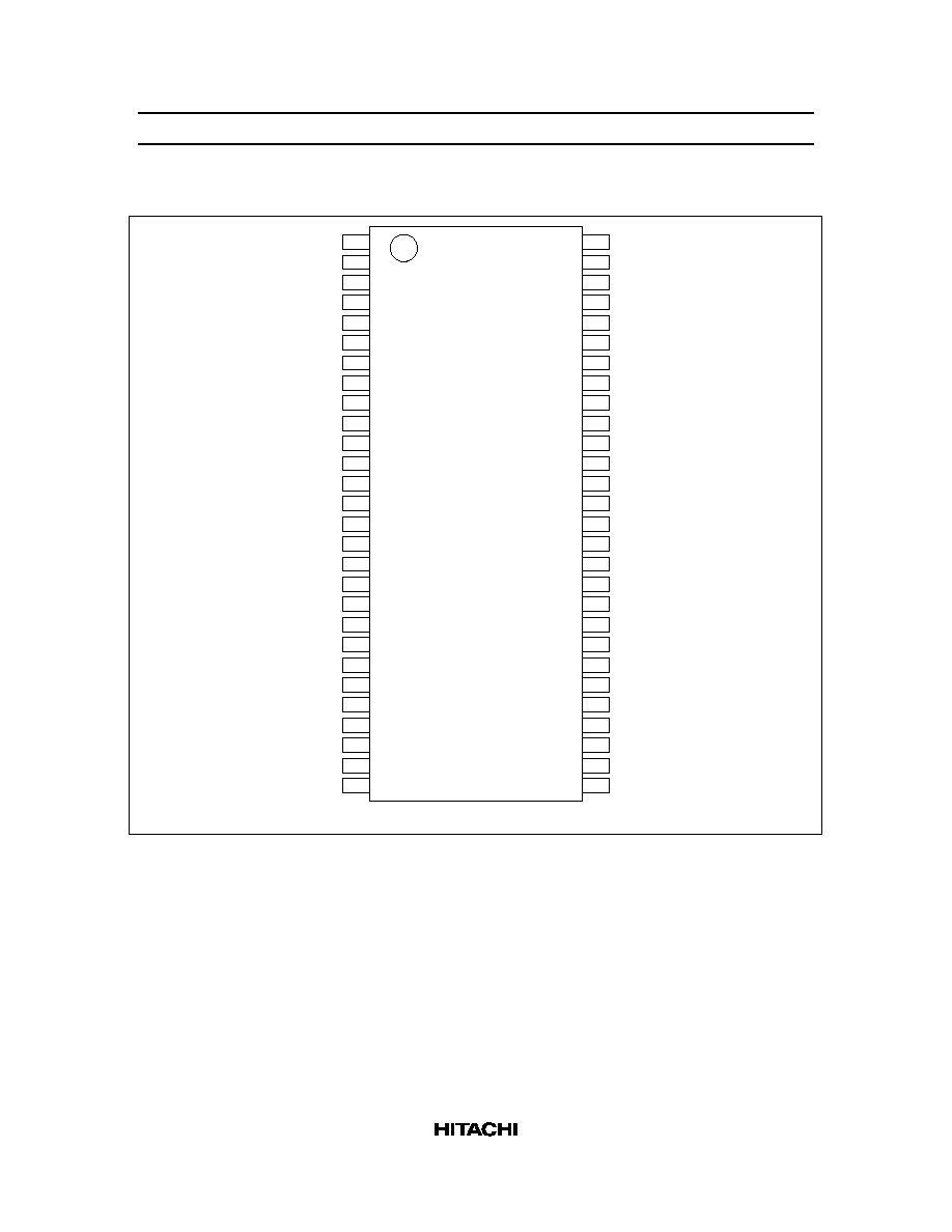
Pin Arrangement
GND
TRRREF
TRRIN
NC
NC
NC
TRYLIM
TRYR
TRYF
SLDIN
SLDLIM
RT
CT2
VSS
CT3
CT1
CE
VREGF
VREGS
BRKSEL
PHASE
PC
CT
AGC
VCTL
REFIN
UFIL
GND
1
2
3
4
5
6
7
8
9
10
11
12
13
14
15
16
17
18
19
20
21
22
23
24
25
26
27
28
GND
FCSREF
FCSIN
FCSRS
TRRRS
VFCS
FCSP
FCGND
FCSN
TRRP
TRRN
TRYP
TRYN
VSLD
SLGND
SLDN
SLDP
VBST
B1
B2
RNF
U
V
W
VSPN
WFIL
VFIL
GND
(Top view)
56
55
54
53
52
51
50
49
48
47
46
45
44
43
42
41
40
39
38
37
36
35
34
33
32
31
30
29

HA13568AT
3
Pin Description
Pin No.
Pin Name
Function
2
FCSREF
FCS driver block reference voltage
3
FCSIN
FCS control input pin
4
FCSRS
FCS sense pin
5
TRRRS
TRR sense pin
6
VFCS
FCS driver and TRR driver power supply
7
FCSP
FCS driver P output
8
FCGND
FCS driver and TRR driver GND
9
FCSN
FCS driver N output
10
TRRP
TRR driver P output
11
TRRN
TRR driver N output
12
TRYP
TRY driver P output
13
TRYN
TRY driver N output
14
VSLD
SLD driver and TRY driver power supply
15
SLGND
SLD driver and TRY driver GND
16
SLDN
SLD driver N output
17
SLDP
SLD driver P output
18
VBST
Booster output pin. This circuit generates a voltage about 1.5 V above that of the
VSPN pin.
19
B1
Booster pumping capacitor connection
20
B2
21
RNF
Spindle driver current detection
22
U
U phase output
23
V
V phase output
24
W
W phase output
25
VSPN
Spindle and booster power supply
26
WFIL
W phase low pass filter. Connect a filter C to this pin during GND.
27
VFIL
V phase low pass filter. Connect a filter C to this pin during GND.
30
UFIL
U phase low pass filter. Connect a filter C to this pin during GND.
31
REFIN
Reference voltage of spindle and slide
32
VCTL
Spindle control input. Generates forward torque when a DC voltage higher than
REFIN is applied, and brake when a DC voltage lower than REF is applied.
33
AGC
For AGC. Holds the level used for IC internal processing fixed even if the B-EMF
level fluctuates due to the rotation speed.
34
CT
Spindle center tap
35
PC
Spindle driver phase compensation

HA13568AT
4
Pin Description (cont)
Pin No.
Pin Name
Function
36
PHASE
Outputs the B-EMF zero cross phase. Open corrector. (See the timing chart)
37
BRKSEL
To select the brake mode. Lo: Short brake, Hi: Reverse full brake
(when forward torque input: BRKSEL = H)
38
VREGS
Voltage regulator sense pin (VREGS
3.3 V output)
39
VREGF
Voltage regulator force pin
40
CE
Chip enable. Input Hi: active
41
CT1
Time constant for clock oscillator circuit. The clock oscillator frequency is
determined by the external capacitor and resistor Ct1 and Rt.
42
CT3
Time constant for PWM carrier oscillator. The carrier frequency is determined by
the external capacitor and resistor Ct3 and Rt.
43
VSS
Control block power supply. 5 V
44
CT2
Time constant for start-up oscillator. The start-up oscillator frequency is
determined by the external capacitor and resistor Ct2 and Rt.
45
RT
Reference voltage (3.3 V). The IC's internal reference current is determined by
this voltage and the external resistor Rt.
46
SLDLIM
SLD output maximum duty setting
47
SLDIN
SLD control input pin
48
TRYF
TRY driver forward input
49
TRYR
TRY driver reverese input
50
TRYLIM
TRY output voltage setting pin
51
NC
No connection
52
NC
53
NC
54
TRRIN
TRR control input pin
55
TRRREF
TRR driver block reference voltage
1, 28, 29, 56, TAB
GND

HA13568AT
5
Block Diagram
Drive
mode
UFIL
W
V
U
Vspn
Tmask
VFIL
WFIL
Vbst
Vbst
VSS
VSPN
AGC
Vref
Vbst
PHASE
VCTL
REFIN
BRKSEL
CT1
CT2
Ct2
RT
Vreg
OTSD
CE
FCSREF
CLK
Ct1
Rt
CLK
OSC
TRRREF
FCSIN
Vbst
U
V
SPN
W
CT
U
V
RNF
PC
B2
B1
W
Rnf
VBST
FCSP
FCSRS
FCSN
VFCS
FCGND
FCS
0.5A
BTL
Vfcs
2
P
N
TRRIN
TRRP
TRRRS
TRRN
TRR
0.5A
BTL
Vfcs
2
P
N
Vbst
SLDIN
SLDLIM
SLDP
SLDN
VSLD
SLGND
SLD
TRY
P
N
VREGS
VREGF
TRYP
TRYN
TRYR
P
N
C102
M
M
TRYF
Ct3
CT3
TAB
42
48
TRYLIM
50
51 ,
,
52
53 : NC pin
49
15
13
14
8
11
5
10
9
7
6
20
19
35
21
24
23
22
34
25
33
43
30
27
26
44
32
31
37
40
45
41
2
55
3
54
47
46
38
39
B-EMF
detection
Commutation
Mask
time
Brake
Start-up
circuit
1.5A
SPN
output
Current
control
Bias
1.5AH
bridge
0.5AH
bridge
SLD
control
36
4
18
17
16
12

HA13568AT
6
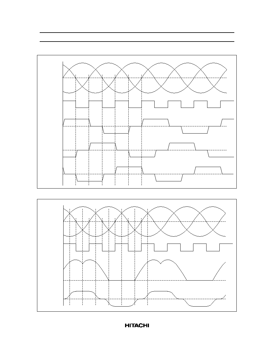
Timing Chart
1. Start-up
CE
CT2
Output
current
(U phase)
Output
current
(V phase)
Output
current
(W phase)
0
-
+
-
+
0
0
0
-
+
0
PHASE
0
4Tc2
2Tc2
4Tc2
4Tc2
4Tc2
4Tc2
6Tc2
8Tc2
10Tc2
12Tc2
14Tc2
16Tc2
B-EMF
Mask period
Synchronous mode
B-EMF mode
Tc2
Vhct2
Vlct2
Note: Tc2 is as follows.
Where,
Vhct2
Vlct2
: CT2 pin high voltage (See electrical characteristics)
: CT2 pin low voltage (See electrical characteristics)
Tc2 =
8 (Vhct2
-
Vlct2) Rt Ct2
Vrt
HA13568AT
7
2. Acceleration (switching mode)
U
V
W
PHASE
Output
current
(U phase)
Output
current
(V phase)
Output
current
(W phase)
0
Reverse
start-up
voltage
B-EMF
0
-
-
+
0
0
-
+
0
-
+
+
3. Running (soft switching mode)
0
PHASE
0
0
-
+
-
+
0
U
V
W
Output
voltage
(U phase)
Output
current
(U phase)
Reverse
start-up
voltage
B-EMF

HA13568AT
8
Truth Table
Table 1
Overall
CE
OTSD
SPN Driver
FCS Driver
TRR Driver
SLD Driver
TRY Driver
L
X
Z
Z
Z
Z
Z
H
ON
Z
Z
Z
Z
Z
OFF
ON
ON
ON
ON
ON
Note:
X: Option, Z: Hi impedance
Table 2
SPN Driver
BRKSEL
VCTL
SPN Driver
X
> REFIN
Forward torque
REFIN
Z
L
< REFIN
Short brake
H
REFIN ≠ 0.6 V
Reverse brake
Note:
X: Option, Z: Hi impedance
Table 3
TRY Driver
TRYF
TRYR
P Output
N Output
L
L
Z
Z
L
H
L
H
H
L
H
L
H
H
H
H
Note:
Z: Hi impedance

HA13568AT
9
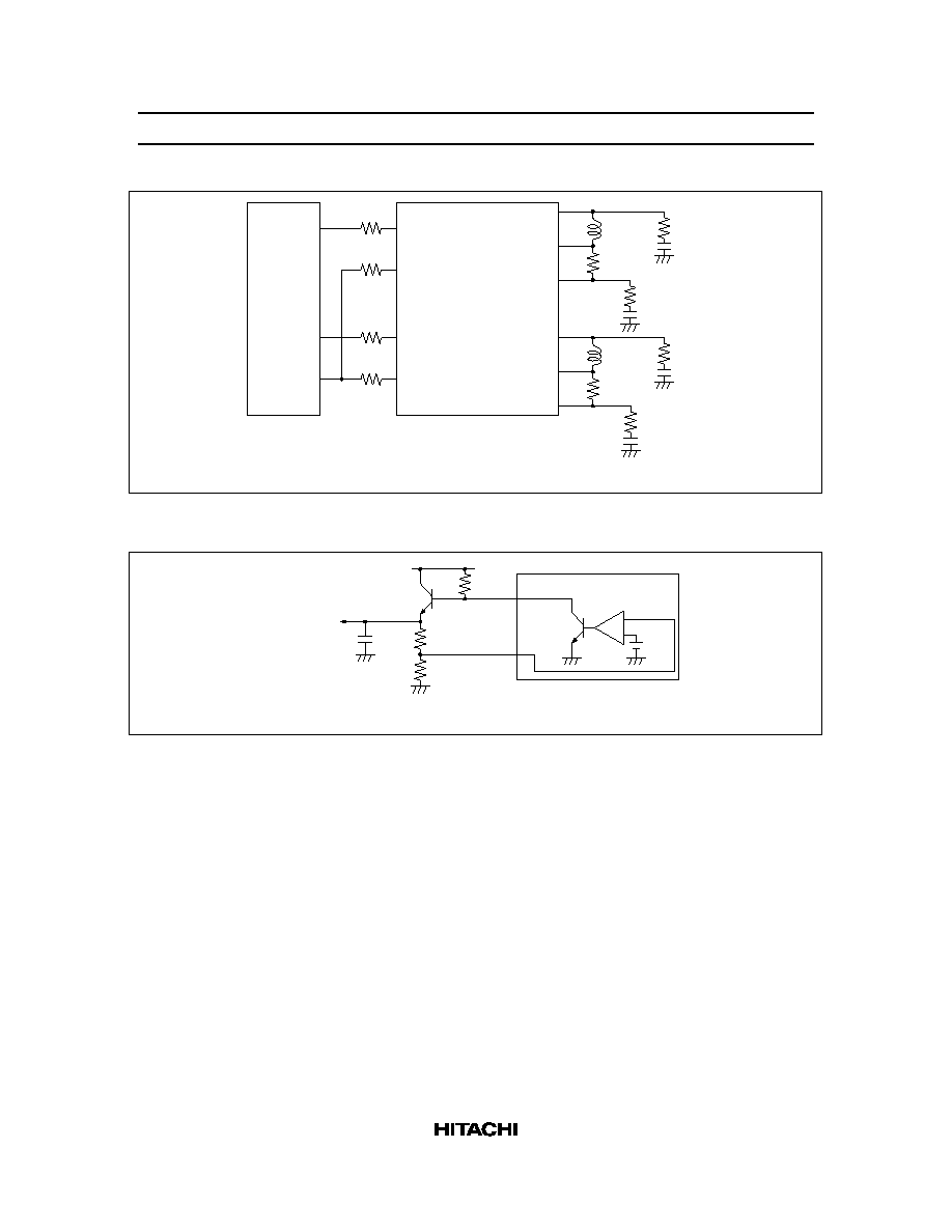
Application
1. FCS, TRR voltage drive
VSPN
VSS
TAB
Vcc
C103
UFIL
C104
VFIL
C105
WFIL
Ct2
5V
C109
Rt2
VREF
FOO
TRO
FMO
3.3V
Q1
CT2
VREGF
VREGS
PHASE
CT1
CE
BRKSEL
VCTL
RT
SLDLIM
C102
AGC
SPN
W
RNF
PC
B1
B2
CT
U
V
+12V
+5V
R106
R107
FCS
R103
C111
+5V
REFIN
DMO
FCSIN
TRYF
TRRIN
FCSREF
TRRREF
SLDIN
CT3
TRYR
TRYLIM
MPU
Ct3
Ct1
C108
C101
C107
Rt1
Rnf
R101
C110
R102
VBST
VFCS
FCSP
FCSRS
FCSN
TRRP
TRRRS
TRRN
FCGND
VSLD
SLDP
SLDN
TRYP
TRYN
SLGND
C106
TRR
SLD
TRY
M
M
Cpc
R105
R104
C112
R110
R111
R112
R113
HA13568AT
10
2. FCS, TRR voltage drive
Note: Other pins have the same connections as those used in application 1.
FCS
RSFCS
FCSP
FCSRS
FCSN
TRRP
TRRRS
TRRN
FCSIN
(Zin
12k
)
FCSREF
(Zin
12k
)
TRRIN
(Zin
12k
)
TRREF
(Zin
12k
)
TRR
R109
C114
RSTRR
R104
C112
R108
R110
R111
R112
R113
C113
R103
C111
FO
DSP
TO
REF
3. When used at a voltage other than 3.3 V with a voltage regulator (Vout = 3.3 to Vcc ≠ 1 V)
Note: Other pins have the same connections as those used in application 1.
Vcc (5V or 12V)
C115
Q1
VREGF
+
-
Vout
Rr2
Rr1
3.3V
3.3V
VREGS
R105

HA13568AT
11
External Components
Parts No.
Reccomended
Value
Reccomended
Range
Purpose
Note
R101
47 k
47 k
Filter for SPN driver control input
R102
47 k
47 k
Filter for SLD driver control input
R103
6.8
--
To stop FCS block oscillation
R104
6.8
--
To stop TRR block oscillation
R105
500
100
for Q1 bias
R106
20 k
--
for TRY driver output voltage setting
R107
27 k
--
R108
6.8
--
To stop FCS block oscillation
R109
6.8
--
To stop TRR block oscillation
R110 to
R113
20 k
--
for BTL gain setting
7
Rnf
0.25
0.25
SPN driver current detection resistor
1
Rt1
1.8 k
Rt1 + Rt2 =
10 k
Reference current setting and SLD driver
maximum duty setting
2, 5
Rt2
8.2 k
RSFCS
1
0.33
for FCS driver current sense
7
RSTRR
1
0.33
for TRR driver current sense
Rr1
--
--
Voltage regulator division resistor
8
Rr2
--
--
C101
0.1
µ
F
0.1
µ
F
for Power supply by passing
C102
0.047
µ
F
for B-EMF Amplitude AGC
C103
0.01
µ
F
for B-EMF filter
6
C104
C105
C106
0.22
µ
F
0.22
µ
F
for Booster pumping
C107
0.47
µ
F
0.47
µ
F
for Booster output smoothing
C108
0.1
µ
F
for SPN driver phase compensation
C109
0.01
µ
F
Filter for SPN control input
C110
3300 pF
Filter for SLD control input
C111
0.01
µ
F
--
To stop FCS block oscillation
C112
0.01
µ
F
--
To stop TRR block oscillation
C113
0.01
µ
F
--
To stop FCS block oscillation
C114
0.01
µ
F
--
To stop TRR block oscillation
C115
2.2
µ
F
for Voltage regulator smoothing

HA13568AT
12
External Components (cont)
Parts No.
Reccomended
Value
Reccomended
Range
Purpose
Note
Ct1
150 pF
120 pF
Time constant for CLK oscillation. Use a
capacitor with good temperature characteristics.
3
Ct2
0.033
µ
F
Time constant for start-up oscillation. Use a
capacitor with good temperature characteristics.
4
Ct3
470 pF
390 pF
PWM carrier oscillation time constant
5
Q1
Transistor for voltage regulator
Note:
1. The output current maximum value Iospnmax of SPN driver is controlled according to the
following equation. However, Vspncl is the current limiter reference voltage. (See the electrical
characteristics)
Iospnmax =
Vspncl
Rnf
2. The maximum duty Dmax of SLD driver output is controlled according to the following equation.
Vrt
Vhct3
-
Vlct3
Rt2
Rt
Vlct3
Vrt
Dmax =
-
◊
100 (%)
However,
Rt2
Rt
Vlct3
Vrt
Rt = Rt1 + Rt2,
Where, Vrt
: RT pin voltage (See the electrical characteristics)
Vlct3 : CT3 pin low voltage (
1.3 V)
Vhct3 : CT3 pin high voltage (
3.3 V)
Since Vrt
Vhct3, Dmax is not limited at 100% when Rt1 = 0
.
3. The CLK oscillation frequency is determined by the following equation.
Vrt
8 Ct1 Rt
Vct1
fclk =
Vrt
8 Ct1 Rt
Vct1
fclk =
Where, Vrt
: RT pin voltage (See the electrical characteristics)
Vct1 : CT1 pin voltage amplitude (
1 V)
4. The Ct2 for start-up oscillation is determined by the following equation.
Tc2 =
J
P Kt Ispnmax
1
6
Ct2 =
Tc2 Vrt
8 Rt (Vhct2
-
Vlct2)
Where, J
: Spindle motor inertia (kg ∑ cm ∑ S
2
)
P
: Number of spindle motor poles (Total number of S poles and N poles)
Kt
: Spindle motor torque constant (kg ∑ cm / A)
Vhct2 : CT2 pin high voltage (
3.3 V)
Vlct2 : CT2 pin low voltage (
1.3 V)

HA13568AT
13
5. The PWM oscillation frequency fpwm is determined by the following equation.
fpwm =
Vrt
8 Ct3 Rt (Vhct3
-
Vlct3)
Where, Vhct3 : CT3 pin high voltage (
3.3 V)
Vlct3 : CT3 pin low voltage (
1.3 V)
6. The C103 to C105 for B-EMF filter are determined by the following equation.
21
Rflt
No
P
35
Rflt
No
P
C103
Where, Rfill
: B-EMF detection output resistor (See the electrical characteristics)
No
: Maximum rotation speed (rpm)
7. The FCS and TRR is determined by the following equation.
Gv =
Voltage drive:
R1
Rin + R2
Gm =
Current drive:
R1
((Rin + R2)
Rs)
Where, R1
: Resistor of IC inside (
30k
)
R2
: Resistor of IC inside (
7k
)
Rin
: Resistor value inserted in the input (
)
(R110 to R113)
Rs
: Current sense resistor (
)
8. The output voltage Vout of voltage regulator is determined by the following equation.
Rr1
Rr2
Vout = 3.3 1 +

HA13568AT
14
Absolute Maximum Ratings (Ta = 25
∞
C)
Item
Symbol
Rating
Unit
Note
Supplu voltage
Vss
7
V
1
SPN supply voltage
Vspn
15
V
1
FCS & TRR supply voltage
Vfcs
15
V
1
SLD & TRY supply voltage
Vsld
15
V
1
Input voltage
Vin
0 to Vss
V
2
Vintrylim
Vss to Vsld
V
SPN output current
Iospn
1.5
A
3
FCS & TRR & TRY output current
Iofcs
0.5
A
3
SLD output current
Iosld
1.5
A
3
Power dissipation
P
T
5
W
4
Junction temperature
Tj
160
∞
C
1
Storage temperature range
Tstg
≠55 to +125
∞
C
Note:
1. Operating voltage range is shown below.
Vss = 4.25 to 5.75 V
Vspn = 4.25 to 13.8 V
Vfcs = 4.25 to 13.8 V (However, the output high voltage is clamped at 7 V.)
Vsld = 4.25 to 13.8 V
Tjopr = 0 to +135
∞
C
2. Applied to BRKSEL, VCTL, REFIN, CE, FCSIN, FCSREF, TRRIN, TRRREF, SLDIN, SLDLIM,
TRYF and TRYR.
3. ASO (Area of Safety Operation) of each output transistor is shown below (TBD).
The voltage between Corrector and Emitter Vce (V)
The voltage between Corrector and Emitter Vce (V)
2
10
1
5
20
15
0.5
2.0
1.5
0.2
1.0
0.1
Corrector Current Ic (A)
Corrector Current Ic (A)
ASO of SPN driver
ASO of SLD driver
2
10
1
5
20
15
0.5
2.0
1.5
0.2
1.0
0.1
t = 10ms
t = 1ms
t = 0.1ms
t = 10ms
t = 1ms
t = 0.1ms
4. Thermal resistance is shown below.
j-tab
12
∞
C / W (back side tab soldering area is 70% or more)
j-a
25
∞
C / W (mounted on 4 layer multi glass-epoxy board, back side tab soldering area is
70% or more)

HA13568AT
15
Electrical Characteristics
(Ta = 25
∞
C, Vss = 5 V, Vspn = 12 V, Vfcs = 5 V, Vsld = 12 V)
Item
Symbol
Min
Typ
Max
Unit
Test Conditions
Applicable
Pins
Note
Quiescent current
Iss0
--
0.7
0.9
mA
CE = L
VSS
Ispn0
--
--
0.2
mA
VSPN
Ifcs0
--
--
0.01
mA
VFCS
Isld0
--
--
0.01
mA
VSLD
Iss1
14
20
25
mA
CE = H, VCTL =
VSS
Ispn1
11
15
20
mA
FCSIN = TRRIN =
VSPN
Ifcs1
6
10
15
mA
SLDIN = REFIN,
VFCS
Isld1
--
--
1.0
mA
TRYF = TRYR = L
All load open
VSLD
Iss2
20
33
60
mA
CE = H, VCTL =
VSS
Ispn2
11
30
50
mA
FCSIN = TRRIN =
VSPN
Ifcs2
7
10
15
mA
SLDIN = 5 V,
VFCS
Isld2
≠15
≠1.0
1.0
mA
TRYF, TRYR = H,
L, All load open
VSLD
Logic
Input current
Iince
0
70
100
µ
A
Vin = 0 to 5 V
BRKSEL,
input
Iin
--
--
±
10
µ
A
CE, TRYF,
Low level voltage
Vil
--
--
0.8
V
TRYR
High level voltage
Vih
2.0
--
--
V
Logic
Low level voltage
Vol
--
--
0.4
V
Io = 1 mA
PHASE
output
Leak current
Icer1
--
--
±
10
µ
A
Vce = 15 V
SPN
driver
Output saturation
voltage
Vsatspn
--
1.25
1.75
V
Iospn = 1.0 A
U, V, W
1
Leak current
Icer2
1.3
2.2
3
mA
Vce = 15 V
Current limiter
voltage
Vspncl
238
265
292
mV
Rnf = 0.25
RNF
2
FCS
Input resistance
Rinfcs
9.6
12
14.4
k
FCSIN
driver
Rinfcsref
9.6
12
14.4
k
Input voltage range
Vinfcs
0
--
5
V

HA13568AT
16
Electrical Characteristics
(Ta = 25
∞
C, Vss = 5 V, Vspn = 12 V, Vfcs = 5 V, Vsld = 12 V) (cont)
Item
Symbol
Min
Typ
Max
Unit
Test Conditions
Applicable
Pins
Note
FCS
driver
Output quiescent
voltage
Vqfcs
2.375
2.5
2.625
V
FCSIN=FCSREF=
2.5 V, VFCS=5 V
FCSP,
FCSN
3
Output offset
voltage
Vosfcs
--
--
±
20
mV
Output saturation
voltage
Vsatfcs
--
1.0
1.4
V
Io = 0.33 A
1
Voltage gain
Gvfcs
11.6
12.6
13.6
dB
4
Gain band width
Bfcs
100
--
--
kHz
Gv = ≠3 dB
TRR
Input resistance
Rintrr
9.6
12
14.4
k
TRRIN
driver
Rintrrref
9.6
12
14.4
k
Input voltage range
Vintrr
0
--
5
V
Output quiescent
voltage
Vqtrr
2.375
2.5
2.625
V
FCSIN=TRRREF=
2.5 V, VFCS=5 V
TRRP,
TRRN
3
Output offset
voltage
Vostrr
--
--
±
20
mV
FCSIN = REF
Output saturation
voltage
Vsattrr
--
1.0
1.4
V
Io = 0.33 A
1
Voltage gain
Gvtrr
11.6
12.6
13.6
dB
4
Gain band width
Btrr
100
--
--
kHz
Gv = ≠3 dB
SLD
driver
Output saturation
voltage
Vsatsld
--
1.5
2.0
V
Iosld = 0.75 A
SLDP,
SLDN
1
Leak current
Icer3
--
--
±
100
µ
A
Vce = 15 V
Penetration current
Iovlap
--
--
100
mA
VSLD
8
Transient response
tplh1
--
--
5
µ
s
SLDP,
time
tphl1
--
--
5
µ
s
SLDN
TRY
driver
Output saturation
voltage
Vsattry
--
1.0
1.4
V
Iotry = 0.33 A
TRYP,
TRYN
1
Leak current
Icer3
--
--
±
100
µ
A
Vce = 15 V
Penetration current
Iovlap
--
--
100
mA
VSLD
8
Transient response
tplh1
--
--
5
µ
s
TRYP,
time
tphl1
--
--
5
µ
s
TRYN
Input current
Iintrylim
--
--
±
5
µ
A
Vtrylim=7 to VSLD
Output voltage
Vlimtry
0.1
0.7
1.0
V
R
L
= 16
,
Vtrylim = 7 V
9

HA13568AT
17
Electrical Characteristics
(Ta = 25
∞
C, Vss = 5 V, Vspn = 12 V, Vfcs = 5 V, Vsld = 12 V) (cont)
Item
Symbol
Min
Typ
Max
Unit
Test Conditions
Applicable
Pins
Note
SPN
Input current
Iinspn
--
--
±
5.0
µ
A
Vctl = 0 to Vss≠1V
VCTL,
2
current
REF voltage range
Vref
1.6
--
3.0
V
REFIN
control
Dead zone voltage
Vdzspn
±
50
--
±
120
mV
Vref reference
Current control
gain
Gctl
--
≠12
±
1.5
dB
RNF
Drive
Change threshold
Vctl
--
0.5
±
0.1
V
Vref reference
VCTL
5
mode
voltage
f
PHASE
--
f
CT2
±
50%
Hz
SOFT SW mode
U, V, W
5
SW
SOFT SW
--
<f
CT2
≠20%
Hz
SW mode
B-EMF
detection
Output resistance
Rflt
--
10
±
20%
k
UFIL, VFIL,
WFIL
Threshold voltage
of PHASE
occurrence
Viemf
--
40
±
50%
mVpp
VSPN
Vss + 3V
F
U, V, W
6
--
28
±
50%
mVpp
VSPN
Vss + 3V
F
CLK
RT voltage
Vrt
3.135
3.30
3.465
V
RT
OSC
CLK oscillation
frequency
fclk
210
240
270
kHz
Rt = 10 k
,
Ct1 = 82 pF
CT1
Start-up
circuit
Start-up oscillation
frequency
fct2
437
485
534
Hz
Rt = 10 k
,
Ct2 = 0.033
µ
F
CT2
SLD
Input current
I
insld
--
--
±
5.0
µ
A
Vsld = 0 to Vss≠1V
SLDIN
control
Input voltage range
Vinsld
0
--
4.0
V
Limiter input
current
Isldlim
--
--
±
5.0
µ
A
SLDLIM
PWM oscillation
frequency
fpwm
33
38
42.35
kHz
Rt = 10 k
,
Ct3 = 470 pF
Control gain
D/V
80
90
100
%/V
7
Offset voltage
Vossld
--
--
20
mV
SLDIN = REFIN
Voltage
regulator
Output sink current
Isinkreg
8.5
12.2
--
mA
VREGS = 4 V,
VREGF = 4 V
Output voltage
Voutreg
3.135
3.30
3.465
V
OTSD
Operating
temperature
Tsd
135
160
--
∞
C
8
Hysteresis
Thys
--
50
--
∞
C
HA13568AT
18
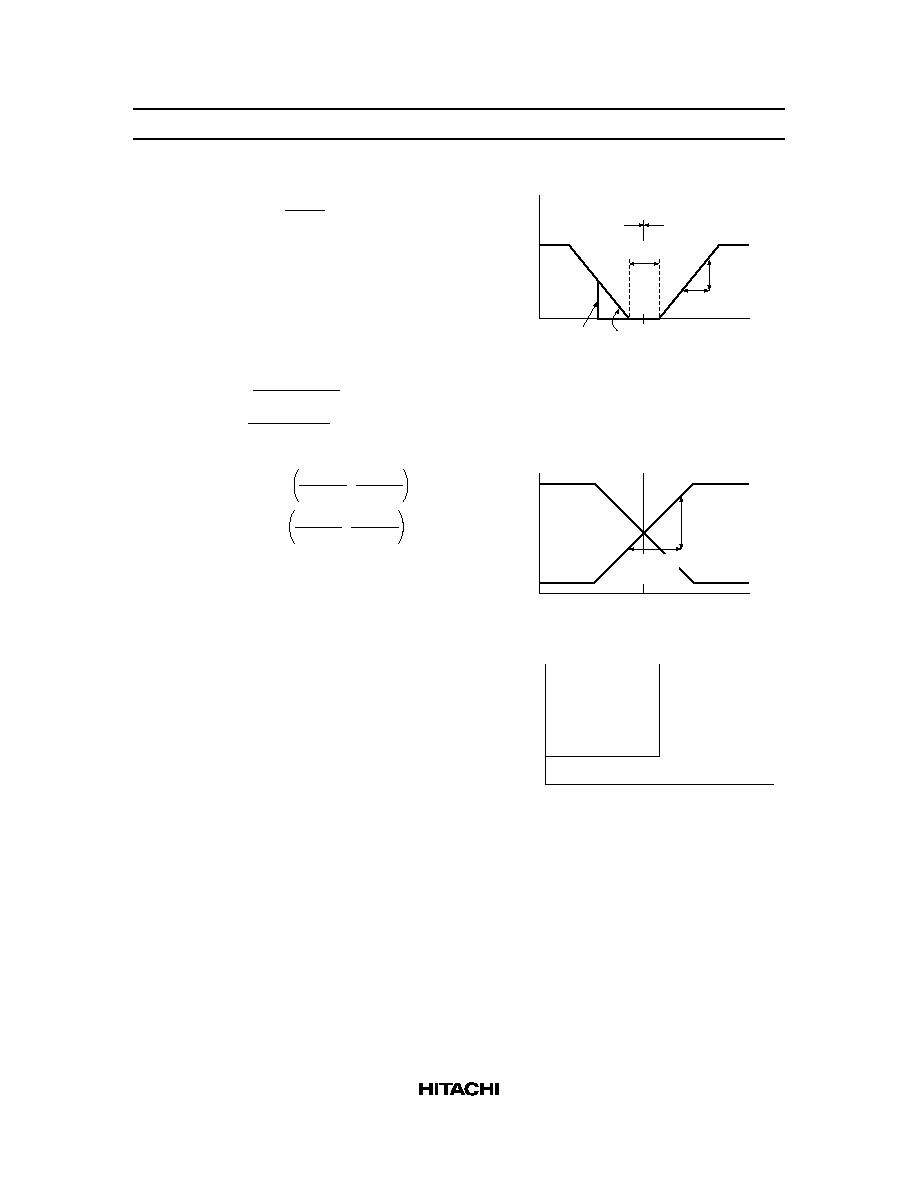
Note:
1. The output saturation voltage is the sum of the upper and lower saturation voltages.
2. See figure 1. Where,
Vspncl
Vref
Reverse
torque
Forward
torque
0
Vctl (V)
Vrnf (V)
Vdzspn
Gctl = 20 log
Vrnf
Vctl
Vrnf
Vctl
Figure 1
Reverse brake Short brake
3. Where,
Vqfcs =
Vfcsp + Vfcsn
2
Vqtrr =
Vtrrp + Vtrrn
2
4. See figure 2. Where,
Vref
0
Vfcsin (Vtrrin)
Vfcsp (Vtrrp) &
Vfcsn (Vtrrn)
Gvfcs = 20 log
Vfcsp
Vfcsin
Vfcsn
Vfcsin
Gvtrr = 20 log
Vtrrp
Vtrrin
Vtrrn
Vtrrin
Vfcsn (Vtrrn)
Vfcsp (Vtrrp)
Vfcsin
(
Vtrrin)
Vfcsp
(
Vtrrp)
Figure 2
5. The circuit operates in soft switching drive mode only when the control input (Vctl) is lower than
f
CT2
and f
PHASE
is higher than the threshold voltage. See figure 3.
0.5V
f
CT2
0
V
CTL
-
REFIN
SW mode
f
PHASE
(Hz)
,
,,
SOFT SW mode
SW mode
Figure 3
6. PHASE is output only when B-EMF exceeds the threshold voltage.
HA13568AT
19
7. See figure 4. Where,
D/V =
D
Vin
100
SLDP = PWM
SLDN = H
SLDP = H
SLDN = PWM
D
Vin
Vref
0
Vinsld (V)
Duty
(%)
Figure 4
8. Design guide only.
9. Vlimtry = VTRYP ≠ VTRYLIM, or VTRYN ≠ VTRYLIM

HA13568AT
20
Reference Data
Output Current Iospn (A)
1.0
0.5
0
1.5
3
1
2
0
Output Saturation Voltage Vsatspn (V)
SPN Driver Output Saturation Voltage vs.
Output Current
FCS Driver Output Saturation Voltage vs.
Output Current
Output Current Iofcs (A)
Output Saturation Voltage Vsatfcs (V)
0.4
0.2
0
0.6
3
1
2
0
Output Current Iosld (A)
1.0
0.5
0
1.5
4
3
1
2
0
Output Saturation Voltage Vsatsld (V)
SLD Driver Output Saturation Voltage vs.
Output Current
TRR Driver Output Saturation Voltage vs.
Output Current
Output Current Iotrr (A)
Output Saturation Voltage Vsattrr (V)
0.4
0.2
0
0.6
3
1
2
0
Output Current Iotry (A)
0.4
0.2
0
0.6
3
1
2
0
Output Saturation Voltage Vsattry (V)
TRY Driver Output Saturation Voltage vs.
Output Current
RT Voltage vs. Junction Temperature
Junction Temperature Tj (
∞
C)
RT Voltage Vrt (V)
75
50
0
25
100
135
3.6
3.2
3.4
3.0
Upper arm, Lower arm
Upper arm, Lower arm
Upper arm + Lower arm
Upper arm + Lower arm
Upper arm, Lower arm
Upper arm + Lower arm
Upper arm, Lower arm
Upper arm + Lower arm
Upper arm, Lower arm
Upper arm + Lower arm
HA13568AT
21
Package Dimensions
0.08
M
0.08
0.17
±
0.05
8.10
±
0.15
0.50
±
0.1
0.65 Max
1
28
29
56
56
29
28
Top view
Under view
1
14.0
6.10
0
∞
-
8
∞
0.50
1.20 Max
0.05
±
0.05
Hitachi Code
JEDEC
EIAJ
Weight (reference value)
TTP-56DT
0.32 g
14.2 Max
0.15
±
0.04
1.0
Unit: mm
0.21
+0.04
-
0.05
0.19
+0.03
-
0.05
(7.5)
(2.8)
Preliminary

HA13568AT
22
Cautions
1. Hitachi neither warrants nor grants licenses of any rights of Hitachi's or any third party's patent,
copyright, trademark, or other intellectual property rights for information contained in this document.
Hitachi bears no responsibility for problems that may arise with third party's rights, including
intellectual property rights, in connection with use of the information contained in this document.
2. Products and product specifications may be subject to change without notice. Confirm that you have
received the latest product standards or specifications before final design, purchase or use.
3. Hitachi makes every attempt to ensure that its products are of high quality and reliability. However,
contact Hitachi's sales office before using the product in an application that demands especially high
quality and reliability or where its failure or malfunction may directly threaten human life or cause risk
of bodily injury, such as aerospace, aeronautics, nuclear power, combustion control, transportation,
traffic, safety equipment or medical equipment for life support.
4. Design your application so that the product is used within the ranges guaranteed by Hitachi particularly
for maximum rating, operating supply voltage range, heat radiation characteristics, installation
conditions and other characteristics. Hitachi bears no responsibility for failure or damage when used
beyond the guaranteed ranges. Even within the guaranteed ranges, consider normally foreseeable
failure rates or failure modes in semiconductor devices and employ systemic measures such as fail-
safes, so that the equipment incorporating Hitachi product does not cause bodily injury, fire or other
consequential damage due to operation of the Hitachi product.
5. This product is not designed to be radiation resistant.
6. No one is permitted to reproduce or duplicate, in any form, the whole or part of this document without
written approval from Hitachi.
7. Contact Hitachi's sales office for any questions regarding this document or Hitachi semiconductor
products.
Hitachi, Ltd.
Semiconductor & IC Div.
Nippon Bldg., 2-6-2, Ohte-machi, Chiyoda-ku, Tokyo 100-0004, Japan
Tel: Tokyo (03) 3270-2111 Fax: (03) 3270-5109
Copyright © Hitachi, Ltd., 1998. All rights reserved. Printed in Japan.
Hitachi Asia Pte. Ltd.
16 Collyer Quay #20-00
Hitachi Tower
Singapore 049318
Tel: 535-2100
Fax: 535-1533
URL
NorthAmerica
: http:semiconductor.hitachi.com/
Europe
: http://www.hitachi-eu.com/hel/ecg
Asia (Singapore)
: http://www.has.hitachi.com.sg/grp3/sicd/index.htm
Asia (Taiwan)
: http://www.hitachi.com.tw/E/Product/SICD_Frame.htm
Asia (HongKong)
: http://www.hitachi.com.hk/eng/bo/grp3/index.htm
Japan
: http://www.hitachi.co.jp/Sicd/indx.htm
Hitachi Asia Ltd.
Taipei Branch Office
3F, Hung Kuo Building. No.167,
Tun-Hwa North Road, Taipei (105)
Tel: <886> (2) 2718-3666
Fax: <886> (2) 2718-8180
Hitachi Asia (Hong Kong) Ltd.
Group III (Electronic Components)
7/F., North Tower, World Finance Centre,
Harbour City, Canton Road, Tsim Sha Tsui,
Kowloon, Hong Kong
Tel: <852> (2) 735 9218
Fax: <852> (2) 730 0281
Telex: 40815 HITEC HX
Hitachi Europe Ltd.
Electronic Components Group.
Whitebrook Park
Lower Cookham Road
Maidenhead
Berkshire SL6 8YA, United Kingdom
Tel: <44> (1628) 585000
Fax: <44> (1628) 778322
Hitachi Europe GmbH
Electronic components Group
Dornacher Straþe 3
D-85622 Feldkirchen, Munich
Germany
Tel: <49> (89) 9 9180-0
Fax: <49> (89) 9 29 30 00
Hitachi Semiconductor
(America) Inc.
2000 Sierra Point Parkway
Brisbane, CA 94005-1897
Tel: <1> (800) 285-1601
Fax: <1> (303) 297-0447
For further information write to: