 | –≠–ª–µ–∫—Ç—Ä–æ–Ω–Ω—ã–π –∫–æ–º–ø–æ–Ω–µ–Ω—Ç: HA13605A | –°–∫–∞—á–∞—Ç—å:  PDF PDF  ZIP ZIP |

HA13605A
Three-Phase Brushless Motor Driver
ADE-207-201A (Z)
2nd. Edition
February, 1998
Description
The HA13605A is a three-phase brushless motor driver IC that provides digital speed control on chip. It
was developed for use as the drum motor driver in plain paper copiers and has the following functions and
features.
Functions
∑
Three-phase output circuit that can provide a maximum of 4.5 A at 35 V per phase
∑
Digital speed control
∑
Crystal oscillator circuit (10 MHz maximum)
∑
FG amplifier
∑
Speed monitor (lock detection output)
∑
Current control circuit
∑
Overvoltage protection circuit (OVSD)
∑
Thermal protection circuit (OTSD)
∑
Low voltage protection circuit (LVI)
∑
Forward/reverse switching circuit
Features
∑
High breakdown voltage, large currents
∑
Direct PWM drive outputs
∑
Employs DMOS
∑
Low on resistance: 0.7
/DMOS maximum
∑
No lower arm flywheel diode is required

HA13605A
2
Pin Description
Pin No.
Pin Name
Function
1
V
CC
Power supply
2
UOUT
U phase output
3
BOOSTL
Booster pin. (Low side)
4
VOUT
V phase output
5
RNF
Output current detection
6
WOUT
W phase output
7
BOOSTH
Booster pin. (High side)
8
UIN
U phase input
9
VR1
Charge pump reference voltage pin.
10
VIN
V phase input
11
V
X1
Output current control voltage input pin.
12
WIN
W phase input
13
C-PMP
Charge pump output pin. Speed error integration and phase compensation
of speed control.
14
FGIN-
FG Amp. (-) input pin
15
FGOUT
FG Amp. output pin
16
FGIN+
FG Amp. (+) input pin
17
DIR
Direction, Rotation direction set up pin
18
PWMOSC
PWM oscillator input pin. Set oscillator frequency.
19
DSEL
Divide select pin (L : 1/3, M : 1/12, M : 1/6)
20
OSCOUT
Oscillator output
21
READY
Ready pin. Speed monitor pin. (open-collector)
22
OSCIN
Oscillator input
23
GND
Ground
HA13605A
3
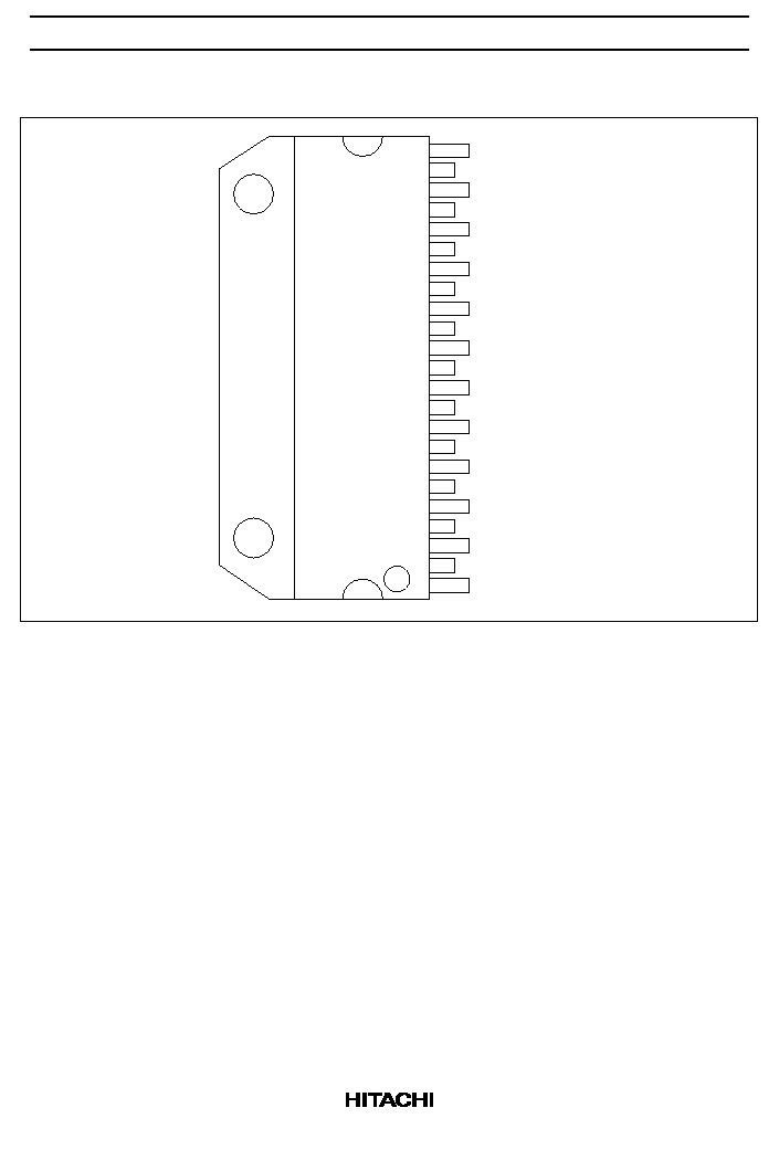
Pin Arrangement
23
22
21
20
19
18
17
16
15
14
13
12
11
10
9
8
7
6
5
4
3
2
1
GND
OSCIN
READY
OSCOUT
DSEL
PWMOSC
DIR
FGIN+
FGOUT
FGIN≠
C-PMP
WIN
V
X1
VIN
VR1
UIN
BOOSTH
WOUT
RNF
VOUT
BOOSTL
UOUT
V
CC

HA13605A
4
Block Diagram
1
7
3
2
4
6
5
11
18
21
13
9
23
19
20
22
14
16
15
17
12
10
8
+
≠
+
≠
+
≠
+
≠
+
≠
≠
+
V
CC
C110
D1
D2
D3
U
V
W
Reference
voltage
Booster
Phase
switching
logic
Control
logic
Pre-
driver
Current
limiter
Filter
FG detector
Noise
filter
Speed
monitor
Divider D
Discriminator
2048
Charge
pump
READY
(open
collector)
Clamping
circuit
D switching
L: 1/3
M:1/12
H: 1/6
R
NF
V
X1
Ct
C2
R2
C1
(
5 V)
R1
TAB
OUT
C108
X'tal
R108
IN
OSC
C107
1/24 fc
23 k
20 k
23 k
V
REF
PWM
OSC
R104
C106
C105
R103
R106
D4
R105
5 V
CE
DIR
LVI
OTSD
OVSD
200 k
(typ.)
5.6 V
R102
C103
HW
HV
HU
C102
C101
R101
C104
C109
R107
H
L
U
H
U
L
V
H
V
L
W
H
W
L
5 V
HA13605A
5
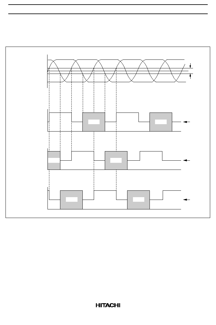
Timing Chart
FWD Mode
0
+
≠
0
0
0
Hu
Hv
Hw
Vhys
OFF
OFF
OFF
PWM
PWM
PWM
PWM
PWM
PWM
Hall amplifier
input
U output
V output
W output
HA13605A
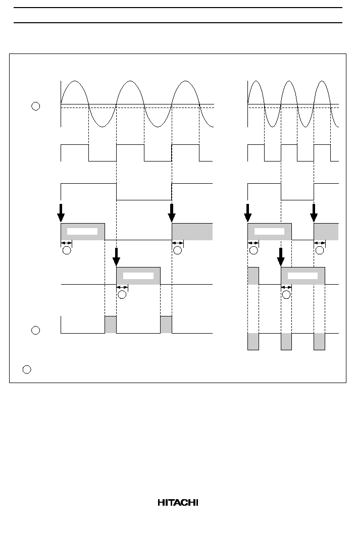
6
Speed control
Hysterisis
Wave
commutation
1/2 frequency
division
FGout
( 15 pin)
2048count
M
M
M
1st. count
2nd. count
2048count
Charge pump
output
( 13 pin)
2048count
M
M
M
2048count
Acceleration pulse
(1) Slow speed
(2) Fast speed
Slowdown pulse
M : Noise cancellation (512count)

HA13605A
7
Truth Value Table
Hall Amplifier Input
Output
DIR Input
U-V
V-W
W-U
U
V
W
H (stop)
X
X
X
Z
Z
Z
M (reverse)
H
L
H
PWM
H
Z
H
L
L
PWM
Z
H
H
H
L
Z
PWM
H
L
H
L
H
PWM
Z
L
H
H
H
Z
PWM
L
L
H
Z
H
PWM
L (forward)
H
L
H
H
PWM
Z
H
L
L
H
Z
PWM
H
H
L
Z
H
PWM
L
H
L
PWM
H
Z
L
H
H
PWM
Z
H
L
L
H
Z
PWM
H
Divider Selector
DSEL
D
H
1/6
M
1/12
L
1/3

HA13605A
8
External Components
Part No.
Recommended Value Purpose
Notes
R1, R2
--
Integration constants
1
R101, R102
--
Hall bias
9
R103, R104
--
FG amplifier gain setting
2, 8
R105, R106
10 k
Used in interfacing
R107
4.7 k
Booster stabilization
11
R108
--
Oscillator feedback resistor
10
R
NF
--
Current detection
3
C1, C2
--
Integration constants
1
C101, C102, C103
0.047
µ
F
Stabilization
C104
0.1
µ
F
Power supply bypass
C105
--
Determines the FG amplifier band
5
C106
--
FG amplifier AC coupling
6
C107, C108
--
Oscillator circuit elements
10
C109
300 pF
Booster capacitance
11
C110
47
µ
F
Stabilization
Ct
--
PWM oscillator time constant
4
X'tal
--
CLK oscillator
7
D1, D2, D3
--
Regenerative current path
D4
--
Used in interfacing
Notes: 1. Use the following formulas to determine target values for these constants.
o
2
f
FG
20
(rad/s)
R2
R1
1
o
R2
=
7.7J
o
NoRmVosc
K
T
V
R1
(2Vps ≠ 0.83V
E
)
3.0 k
R1
15 k
C1 =
1
10
∑
(F)
C2 = 10C1
(F)
Where:
o:
Control loop angular frequency
f
FG
:
FG frequency
(Hz)
J:
Moment of inertia of the motor
(kg∑m
2
)
No:
Rotation speed
(rad/s)
Rm:
Motor coil resistance
(
/T∑T)
K
T
:
Torque constant
(N∑m/A)
V
E
:
Motor reverse voltage at speed No
(V
PP
/T∑T)
Vps: Power supply voltage
(V)
Vosc: PWM oscillator amplitude
2.2 (V
PP
: See the electrical characteristics table.)
HA13605A
9
V
R1
:
Charge pump reference voltage
5.6 (V: See the electrical characteristics table.)
2. The voltage gain (Gfg) of the FG amplifier is determined by the following formula. Here Rfgf is
the internal feedback resistance. See the electrical characteristics table.
However, note that R103 must be equal to R104.
Gfg =
Rfgf
R103
3. The output current limit is given by the following formula.
Iomax =
(V
X1
-- 25 mV)
Rnf
(A)
4. The PWM carrier frequency is determined by the following formula. Here VR1 and K are the
charge pump voltage and the oscillator amplitude (see the electrical characteristics table),
respectively.
f
P
=
VR1
KCt R1 V
OSC
(Hz)
.
.
5. The FG amplifier bandwidth BW is determined by the following formula. Here Rfgo is the pin 15
output resistance. See the electrical characteristics table.
However, when C105 is 0, BW is limited to 8 kHz by the internal capacitance.
BW =
1
2
C105 Rfgo
(Hz)
6. Determine C106 using the following formula as a rough estimate.
C106
1
(R103 + R104) f
FG
(F)
Consult with the oscillator element manufacturer.
7. Relationship of between the CLK frequency fc and the FG frequency f
FG
. Are determined by the
under table.
2048.5 ∑
f
FG
D
f
FG
D
2048.5 ∑
fc (Hz)
But rotation response is 80 ppm down
1/3
D
1/6
1/12
8. If an input of 1.25/G
FG
(Vp-p) or higher is applied, irregular rotation may occur due to FG amplifier
saturation.
9. The absolute value of the whole amplifier input voltage must be within the in-phase input voltage
range.
10. This should be decided after consultation with the oscillator manufacturer.
11. Determine C109 using the following formula as a rough estimate.
300pF
<
C109
(F)
20
Fc (R108 + 200
)
3 k
R107
6 k

HA13605A
10
12. TAB should be connected to pin 23 (GND). The FG amplifier may not operate normally, causing
irregular rotation, due to parasitism during phase switching.
Absolute Maximum Ratings (Ta = 25
∞
C)
Item
Symbol
Rated Value
Unit
Notes
Power supply voltage
V
CC
45
V
1
Input voltage (1)
Vin(1)
≠0.3 to 6
V
2
Input voltage (2)
Vin(2)
≠0.3 to 6
V
3
Instantaneous output current
Iomax
4.5 (@T
400 ms)
A
4
Steady state output current
Iout(1)
1.5
A
4
Logic output current
Iout(2)
10
mA
5
Output voltage
Vout
15
V
5
Allowable power dissipation
P
T
25 (@Tc = 112
∞
C)
W
6
Operating junction temperature
Tjopr
≠10 to +125
∞
C
Storage temperature
Tstg
≠55 to +125
∞
C
Notes: 1. The operating voltage range is as shown below.
V
CC
= 20 to 35 V
2. Applies to the hall amplifier. (Pin 8, Pin 10, Pin 12)
3. Applies to the DIR input pin (Pin 17) and the D switchover input pin (Pin 19).
4. Applies to the U, V, and W output pins (Pins 2, 4, and 6). The operation locus of each TRS must
not exceed the ASO range shown in figure 1.
However, there is no particular regulation concerning the recovery current. Refer to figure 2 for
the temperature rise in the event of rush.
5. Applies to the speed monitor output (Pin 21).
6. The package thermal resistances are shown below.
j-c
1.5
∞
C/W (with an arbitrarily large heat sink)
j-a
35
∞
C/W (when mounted on a glass-epoxy PC board)

HA13605A
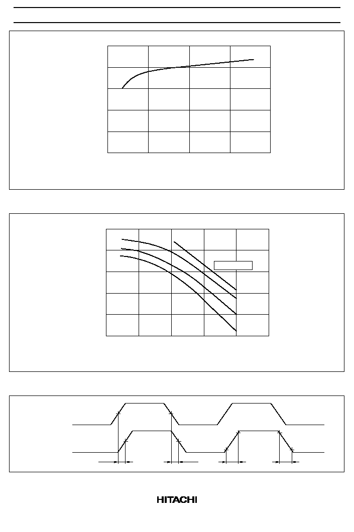
11
1
10
100
45
0.1
1
10
4.5
1.5
1 shot pulse
(@Ta = 25∞C)
I
D(MAX)
(@T
C
= 75∞C)
DC operation
Pw = 0.1 ms
Pw = 1.0 ms
Pw = 10 ms
VDS [V]
Iout (1) [A]
Figure 1 ASO Range
0.2
0.4
0.6
0.8
1.0
1.2
4
3
2
1
0
Rush current 5 A
4 A
3 A
Rush Time [s]
Temperature Rising [∞C]
(Design guide only)
Figure 2 Rush Time vs. Temperature Rising

HA13605A
12
Electrical Characteristics (Ta = 25
∞
C, V
CC
= 24 V)
Item
Symbol Min
Typ
Max
Unit
Test Conditions
Applicable
Pins
Notes
Current drain
Icc(1)
--
--
18
mA
V
CC
= 35 V
R1 = 5.6 k
Icc(2)
--
--
20
mA
V
CC
= 45 V
Hall
Input current
Ih
--
--
±
20
mA
8, 10, 12
amplifier
Common mode
input voltage
range
Vhc
1.5
2.5
3.5
V
Differential mode
input voltage
range
Vhd
50
--
1000
mV
PP
Output
Leakage current
Icer
--
--
3
mA
Vds = 35 V
2, 4, 6
amplifier
On resistance
Rdson
--
0.5
0.7
Io = 1.5 A, Tj = 25
∞
C
1
Diode voltage
Vfl
--
1.2
2.0
V
I
F
= 1.5 A, lower arm
Vfu
0.8
1.2
--
V
I
F
= 1.5 A, upper arm
PWM
Low level voltage
VI
1.10
1.30
1.50
V
18
oscillator
& Com-
Oscillator
amplitude
Vosc
2.0
2.2
2.4
V
PP
parator
Correct coefficient K
12
14
16
--
R1 = 5.6 k
FG
amplifier
Input voltage
range
Vfg
8
--
300
mV
PP
Gfg = 32 dB, R103,
R104 = 580
14, 16
and FG
detector
Differential noise
margin
nd
--
--
1.25
mV
PP
Gfg = 32 dB, R103,
R104 = 580
,
Common noise
margin
nc
1.0
--
--
V
PP
f = 1kHz
CLK OSC
Oscillator
frequency range
fc
1.0
--
10.0
MHz
Crystal oscillator
20, 22
Discrimi-
Count
N
--
2048
--
--
nator
Operating
frequency range
fdis
--
--
3.0
MHz
2
Charge
R1 voltage
V
R1
5.1
5.6
6.1
V
R1 = 5.6 k
3
pump
Charge current
Icp
0.117
0.130
0.143
A/A
Vo = 1.5 V,
13
4
Discharge current
Icd
≠0.117 ≠0.130 ≠0.143 A/A
R1 = 5.6 k
Current ratio
IR
0.8
1.0
1.2
A/A
Icp/Icd
Leakage current
Ioff
--
--
±
50
nA
Vo = 3.5 V
Clamp voltage
Vcrmp
4.00
4.25
4.50
V
Icp = 50 mA

HA13605A
13
Electrical Characteristics (Ta = 25
∞
C, V
CC
= 24 V) (cont)
Item
Symbol Min
Typ
Max
Unit
Test Conditions
Applicable
Pins
Notes
Speed
Locking range
No
--
±
5
--
%
21
5
monitor
Output low level
voltage
Vol2
--
--
0.4
V
Io = ≠10 mA
Output leakage
current
Icer2
--
--
±
10
µ
A
Vce = 15 V
Current
Input current
Icl
--
--
±
10
µ
A
Vx1 = 0 to 2 V
11
limiter
Offset voltage
Vclos
≠10
≠25
≠40
mV
Vx1 = 0.5 to 2 V
LVI
Operating voltage
Vsd
--
--
20
V
Turn on
1
OVSD
Operating voltage
Vovs
35
--
--
V
Turn on
1
OTSD
Operating
temperature
Tsd
125
160
--
--
9
Hysteresis
Thys
--
15
--
--
Input
Input current
Ii1, Ii2
≠10
--
40
µ
A
Vin = ≠0.3 V to 5.25 V
interface
DIR Input low
voltage
Vil1
--
--
1.2
V
DIR Input middle
voltage
Vim1
1.7
--
3.2
V
DIR Input high
voltage
Vih1
3.7
--
--
V
D Input low
voltage
Vil2
--
--
1.5
V
D Input middle
voltage
Vim2
2.0
--
2.8
V
D Input high
voltage
Vih2
3.5
--
--
V
Hall amp.
Hysteresis
Uhys
--
20
--
mV
Rh = 400
6, 9
Power
Transient
tphl1
--
--
1
µ
s
at PWM
7, 9
drive
response time
tplh1
--
--
1
µ
s
at PWM
tr, tf
--
--
300
ns
at PWM
Filter
Noise cancellation
range
Tn1
--
1.0
--
µ
s
9
PWMOSC
& comp-
Oscillation
frequency range
fp
2
--
20
kHz
9
arator
Comparator
hysteresis
Vphys
--
50
--
mV
9

HA13605A
14
Electrical Characteristics (Ta = 25
∞
C, V
CC
= 24 V) (cont)
Item
Symbol Min
Typ
Max
Unit
Test Conditions
Applicable
Pins
Notes
FG amp.
& FG
Feedback
resistance
Rfgf
--
23
--
k
9
detector
Output resistance
Rfgo
--
20
--
k
9
Hysteresis
VZXhys
--
≠80
--
mV
9
CLK OSC
Frequency error
Dfc
--
--
±
0.01
%
Crystal oscillator
9
Threshold voltage
Vfth
--
2.7
--
V
9
Oscillation
amplitude
Vfc
--
5.6
--
Vpp
9
OVSD
Hysteresis
OVDhys --
1.5
--
V
9
LVI
Hysteresis
Lhys
--
1.0
--
V
9
Noise filter Noise cancellation
range
Tn2
--
3.0
--
µ
s
fc = 4 MHz, D = 1/6
8, 9
Notes: 1. The on resistance per single MOS transistor.
2. Stipulated for the discriminator input.
3. See figure 3. See figure 4.
4. Specified as a ratio to the R1 current.
5. The speed monitor output is low when the motor is at the set speed.
6. See figure timing chart.
7. See figure 5.
8. Refer to the operation and the formula for determining the maximum cancelable noise width Tn
(figure 6).
Noise cancellation is effective only when the FG detector output is low.
9. Design guide only.
HA13605A
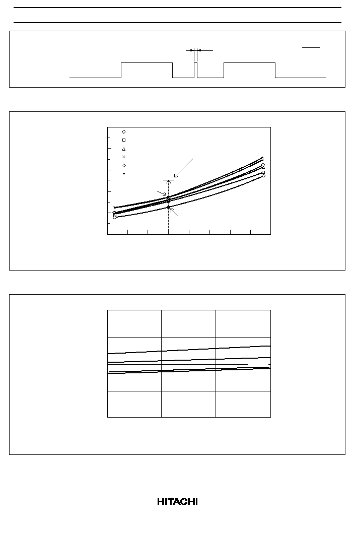
15
0
5
10
15
20
5.3
5.4
5.5
5.6
5.7
R1 [k
]
VR1 [V]
5.2
Tj = 25 ∞C
Figure 3 VR1-R1 Characteristics
-50
0
50
100
150
5.3
5.4
5.5
5.6
5.7
Tj [∞C]
VR1 [V]
5.2
R1
resistance
value
15 k
5.6 k
3 k
≠2.3 mV/∞C
200
Figure 4 VR1 Temperature Characteristics
Pin 18
input voltage
Pin 2, 4, 6
output voltage
tphl
tplh
tr
tf
50%
50%
50%
50%
10%
90%
10%
90%
Figure 5
HA13605A
16
FG detector
output
Tn2 <
3
fc ∑ D
Tn
Figure 6
-50
0
50
100
150
0.4
0.6
0.8
1.0
1.2
Temperature Ta [∞C] = Tj
On resistanse Ron [
]
0.2
Ron max
0.7
(@Iout = 2 A)
-25
25
75
125
0.54
0.47
U-upper
V-upper
W-upper
U-lower
V-lower
W-lower
Figure 7 Ron Temperature Dependence Characteristics
20
35
5
10
15
20
Supply Voltage V
CC
[V]
Quiescent Current I
CC
[mA]
0
25
30
Ta = ≠40∞C
25∞C
125∞C
140∞C
Figure 8 Supply Voltage vs. Quiescent Characteristics

HA13605A
17
Package Dimensions
Unit: mm
M
0.38
30.18 ± 0.25
4.32 ± 0.05
17.50 ± 0.13
Pin No.
1
3
5
7
9 11 13 15 17 19 21 23
2
4
6
8 10
14 16 18 20 22
12
27.94
0.70
+0.09
≠0.1
1.27
10.70 ± 0.12
2 ≠ R1.84 ± 0.19
2.79
¯
3.80 ± 0.05
9.91
19.81
5.08
4.29
0.40
+0.06
≠0.04
17.78 ± 0.25
4.14 ± 0.33
4.50 ± 0.12
1.55
+0.05
≠0.1
3.80 ± 0.05
0.25
0.61
M
0.38
Hitachi code
EIAJ code
JEDEC code
SP-23TE
--
--

Cautions
1. Hitachi neither warrants nor grants licenses of any rights of Hitachi's or any third party's patent,
copyright, trademark, or other intellectual property rights for information contained in this document.
Hitachi bears no responsibility for problems that may arise with third party's rights, including
intellectual property rights, in connection with use of the information contained in this document.
2. Products and product specifications may be subject to change without notice. Confirm that you have
received the latest product standards or specifications before final design, purchase or use.
3. Hitachi makes every attempt to ensure that its products are of high quality and reliability. However,
contact Hitachi's sales office before using the product in an application that demands especially high
quality and reliability or where its failure or malfunction may directly threaten human life or cause risk
of bodily injury, such as aerospace, aeronautics, nuclear power, combustion control, transportation,
traffic, safety equipment or medical equipment for life support.
4. Design your application so that the product is used within the ranges guaranteed by Hitachi particularly
for maximum rating, operating supply voltage range, heat radiation characteristics, installation
conditions and other characteristics. Hitachi bears no responsibility for failure or damage when used
beyond the guaranteed ranges. Even within the guaranteed ranges, consider normally foreseeable
failure rates or failure modes in semiconductor devices and employ systemic measures such as fail-
safes, so that the equipment incorporating Hitachi product does not cause bodily injury, fire or other
consequential damage due to operation of the Hitachi product.
5. This product is not designed to be radiation resistant.
6. No one is permitted to reproduce or duplicate, in any form, the whole or part of this document without
written approval from Hitachi.
7. Contact Hitachi's sales office for any questions regarding this document or Hitachi semiconductor
products.
Hitachi, Ltd.
Semiconductor & Integrated Circuits.
Nippon Bldg., 2-6-2, Ohte-machi, Chiyoda-ku, Tokyo 100-0004, Japan
Tel: Tokyo (03) 3270-2111 Fax: (03) 3270-5109
Copyright ' Hitachi, Ltd., 1999. All rights reserved. Printed in Japan.
Hitachi Asia Pte. Ltd.
16 Collyer Quay #20-00
Hitachi Tower
Singapore 049318
Tel: 535-2100
Fax: 535-1533
URL
NorthAmerica
: http:semiconductor.hitachi.com/
Europe
: http://www.hitachi-eu.com/hel/ecg
Asia (Singapore)
: http://www.has.hitachi.com.sg/grp3/sicd/index.htm
Asia (Taiwan)
: http://www.hitachi.com.tw/E/Product/SICD_Frame.htm
Asia (HongKong)
: http://www.hitachi.com.hk/eng/bo/grp3/index.htm
Japan
: http://www.hitachi.co.jp/Sicd/indx.htm
Hitachi Asia Ltd.
Taipei Branch Office
3F, Hung Kuo Building. No.167,
Tun-Hwa North Road, Taipei (105)
Tel: <886> (2) 2718-3666
Fax: <886> (2) 2718-8180
Hitachi Asia (Hong Kong) Ltd.
Group III (Electronic Components)
7/F., North Tower, World Finance Centre,
Harbour City, Canton Road, Tsim Sha Tsui,
Kowloon, Hong Kong
Tel: <852> (2) 735 9218
Fax: <852> (2) 730 0281
Telex: 40815 HITEC HX
Hitachi Europe Ltd.
Electronic Components Group.
Whitebrook Park
Lower Cookham Road
Maidenhead
Berkshire SL6 8YA, United Kingdom
Tel: <44> (1628) 585000
Fax: <44> (1628) 778322
Hitachi Europe GmbH
Electronic components Group
Dornacher Straße 3
D-85622 Feldkirchen, Munich
Germany
Tel: <49> (89) 9 9180-0
Fax: <49> (89) 9 29 30 00
Hitachi Semiconductor
(America) Inc.
179 East Tasman Drive,
San Jose,CA 95134
Tel: <1> (408) 433-1990
Fax: <1>(408) 433-0223
For further information write to: