 | –≠–ª–µ–∫—Ç—Ä–æ–Ω–Ω—ã–π –∫–æ–º–ø–æ–Ω–µ–Ω—Ç: HA13614FH | –°–∫–∞—á–∞—Ç—å:  PDF PDF  ZIP ZIP |

HA13614FH
Combo (Spindle & VCM) Driver
ADE-207-246D (Z)
Preliminary
5th Edition
October 1998
Description
This COMBO driver for HDD application consists of sensorless spindle driver and BTL type VCM driver.
"PWM soft switching function" for low power dissipation and less commutation acoustic noise at the same
time is implemented by using the IPIC* process.
Note:
I
ntelligent
P
ower
IC
Features
∑
PWM soft switching drive
∑
Small surface mount package: FP-48T
∑
Low thermal resistance: 30
∞
C/W with 4 layer multi glass-epoxy board
∑
Low output on resistance
Spindle
1.2
Typ
VCM
1.4
Typ
∑
TTL compatible input level (with 3.3 V logic interface)
∑
High precision reference voltage output (for 3.3 V power supply)
Functions
∑
16 bit serial port
∑
2.0 A Max/3-phase spindle motor driver with PWM soft switch function
∑
1.5 A Max BTL VCM driver with low crossover distortion
∑
PWMDAC for VCM drive current control
∑
Power off brake function for spindle motor
∑
Auto retract with constant output voltage
∑
Booster
∑
Internal Protector (OTSD, LVI)
∑
Precision power monitor
∑
OP amplifier

HA13614FH
2
Pin Arrangement
1
2
3
4
5
6
36
35
34
33
32
31
30
29
28
27
26
25
OP1OUT
OP1IN(
-
)
OP2IN(+)
Vss
OP2OUT
PC
TABGND
VCMPS
VCMN
Rs
VCMIN
VCMP
VCMSLC
TABGND
TABGND
TABGND
COMM
PHASE
SPNCTL
UFLT
NFLT
VpsIN
VpsOUT
FLTOUT
Vpss
W
ISENSE
CT
POR
LVI1
DELAY
DACOUT
VREF
VIPWMH
VIPWML
12VGOOD
DATA
SEENAB
SCLK
CLK
RETPOW
RETSET
BC1
BC2
Vpsv
VBST
13 14 15 16 17 18
19 20 21 22 23 24
48 47 46 45 44 43
42 41 40 39
37
38
(Top View)
7
8
9
10
11
12
BRKDLY
U
V
RNF
BRK
LVI2

HA13614FH
3
Pin Description
Pin No.
Pin Name
Function
1
OP1OUT
Output of OP amp. 1
2
OP1IN(≠)
Inverted input of OP amp. 1
3
OP2IN(+)
Non-inverted input of OP amp. 2
4
Vss
Power supply for +5 V
5
OP2OUT
Output of OP amp. 2
6
PC
External time costant connection terminal for phase compensation of VCM
driver
7
VCMPS
Current sensing terminal for VCM driver
8
VCMN
Output of VCM driver (Inverted output of VCMP)
9
Rs
Current sensing terminal for VCM driver (differential input for VCMPS)
10
VCMIN
Input of VCM driver (differential input for VREF)
11
VCMP
Output of VCM driver (inverted output of VCMN)
12
VCMSLC
External capacitor connection terminal for stabilizing internal reference
voltage of VCM driver
13
RETPOW
Power supply terminal of retract driver
14
RETSET
Output voltage set up terminal of retract driver
15
BC1
External capacitor connection terminal for pumping of booster
16
BC2
17
Vpsv
+12 V power supply for VCM driver
18
VBST
Output of booster circuit
19
BRKDLY
Time constance set up terminal of delayed brake
20
U
U-phase output of spindle motor driver
21
V
V-phase output of spindle motor driver
22
RNF
Current sensing terminal for spindle motor driver
23
BRK
External capacitor connection terminal for power off brake
24
LVI2
Resistor connection terminal for set up the threshold of +3.3 V power monitor
25
CT
Center tap connection terminal for spindle motor
26
ISENSE
Input of PWM comparator
27
W
W-phase output of spindle motor driver
28
Vpss
+12 V power supply for spindle motor driver
29
FLTOUT
PWMDAC output for current control of spindle motor driver
30
VpsOUT
Output of power supply switch
31
VpsIN
Input of power supply switch (+12 V)
32
NFLT
Output of pre-filter for B-EMF sensing (capacitor connection terminal)
33
UFLT

HA13614FH
4
Pin Description (cont)
Pin No.
Pin Name
Function
34
SPNCTL
PWMDAC input for current control of spindle motor driver
35
PHASE
Toggle signal output for zero-crossing timing of B-EMF
36
COMM
Commutation signal input for spindle motor driver during synchronous driving
37
CLK
Master clock input of commutation logic circuit
38
SCLK
Clock input of serial port for data strobe
39
SEENAB
Enable signal input of serial port
40
DATA
Data signal input of serial port
41
12VGOOD
Output of power monitor for +12 V power supply (open drain)
42
VIPWML
PWMDAC input for current control of VCM driver
43
VIPWMH
44
VREF
Output of internal reference voltage
45
DACOUT
PWMDAC output for current control of VCM driver
46
DELAY
Capacitor connection terminal for set up the power on reset time
47
LVI1
Resistor connection terminal for set up the threshold of +12 V power monitor
48
POR
Output of power on reset signal
TAB
GND
Ground of this IC

HA13614FH
5
Block Diagram
+
-
+
-
37
33
1
128
CLK
CLK
BRK
BRAKE
POR
OTSD
U
UFLT
C101
C112
C116
C102
B-EMF
Amps
V
W
Brake
control
Retract
driver
Spindle
driver
CLK
MASK
OP Amp.1
OP Amp.2
+
-
P
N
B-EMF
PWMOUT
SPN
GAIN
EXTCOM
Commutation
logic
STANDBY
SPNENAB
EXTCOM
BRAKE
VCMENAB
SOFTSW
TEST
SPNGAIN
Serial
input
RESET
VCM
driver
VCMENAB
V
BST
V
BST
Vps Vss
V
BST
V
BST
Selector
Vref(=5.3V)
BIAS
Booster
CLK
TEST
1.4V ref.
44
VREF
PC
C104
C1
29
2
FLTOUT
C103
Input
filter
Power
monitor2
Vss
Power
monitor1
32
NFLT
43
VIPWMH
PWM
decoder
42
45
38
40
39
VIPWML
DACOUT
36
COMM
35
PHASE
34
SPNCTL
(TESTOUT)
1
OP1OUT
3
OP2IN(+)
5
OP2OUT
10
VCMIN
SCLK
DATA
SEENAB
OP1IN(
-
)
C111
23
VpsIN
31
VpsOUT
30
Vpss
BRKDLY
Vss
Vss (+5V)
Vps (+12V)
Vps
(+12V)
Vdd
(+3.3V)
Vss (+5V)
C113
4
Current
control
(PWM)
11
VCMP
12
VCMSLC
VCMN
6
Vpsv
17
RETPOW
13
ISENSE
RETSET
VBST
14
26
RNF
R
NF
22
W
27
V
21
U
20
CT
25
8
VCMPS
7
Rs
9
41
12VGOOD
(Open Drain)
48
POR
(L: RESET)
28
C114
C110
R106
R
S
R
L
C115
R105
R109
18
C107
R103
LVI1
LVI2
R101
R107
R102
R108
DELAY
47
C105
C117
46
BC1
BC2
15
16
TAB
POR
delay
POW DWN
R104 C108
C106
Vss (+5V)
R110
C109
19
24
OTSD
HA13614FH
6
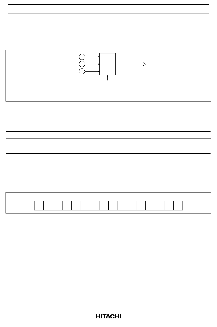
Serial Port
Construction
Serial
port
SEENAB
SCLK
DATA
Note: When
POR
= Low, internal RESET signal becomes High and when RESET = High,
all bit of serial port are set up default value as shown in table 2.
D0 to D15
to each block
RESET *
Figure 1 Construction of Serial Port
Table 1
Truth Table of Internal RESET Signal
I n p u t
O u t p u t
N o t e
POR
RESET
Low
High
1
Open
Low
1
Note:
1. When +5 V or +3.3 V power supply goes to Low, then
POR
= Low.
POR
output is able to construct the wired logic with external signal.
Input Data
D15 D14 D13 D12 D11 D10 D9
D8
D7
D6
D5
D4
D3
D2
D1
D0
MSB
LSB
Figure 2 Input Data
The serial port is required the 16 bits data (D0 to D15). When the data length is less than 16 bits, the
internal register will not be up dated. And when the data length is more than 16 bits, this register will take
later 16 bits and ignore the faster bit.

HA13614FH
7
Bit Assingnment
Table 2
Bit Assingnment of Serial Port
B i t
Symbol
1 (= High)
0 (= Low)
D e f a u l t
N o t e
D0
STANDBY
Active
Stand by
0
1
D1
VCMENAB
VCM enable
VCM disable
0
1
D2
SPNENAB
Spindle enable
Spindle disable
0
1
D3
BRAKE
Brake enable
Brake disable
0
1
D4
SENSEN
B-EMF sense enable
B-EMF sense disable
0
2
D5
VARCNT
Variable count
Normal count
0
2
D6
EXTCOM
External commutation
Internal commutation
0
2
D7
SRCTL1
High slew rate
Low slew rate
0
3
D8
SRCTL2
Commutation time select (See table 4)
0
4
D9
SRCTL3
0
4
D10
OFFTIME1
Off time select of PWM drive (See table 5)
0
5
D11
OFFTIME2
0
5
D12
SPNGAIN
High gain
Low gain
0
6
D13
RETRACT
Retract
Not retract
0
1
D14
TEST1
For testing
0
7
D15
TEST2
0
7
Note:
1. The priority of operation for each bit is as shown in table 3.
2. This bit is using for start up of spindle motor. Please refer to the application note explained
about start up of spindle motor.
3. The slew rate during every commutation of spindle motor is selectable by using this bit. Please
select the suitable value of this bit for your motor.
4. This bit is used for setting up the commutation time (refer to figure 9) of spindle motor as shown
in table 4.
5. This bit is used for setting up the off time at PWM driving of spindle motor as shown in table 5.
6. The gain of current control for spindle motor is selectable by using this bit. Please select the
suitable value of this bit for your motor.
7. This bit will be used in fabrication test. Please set up D15 = "0" normally.
SPNCTL terminal (pin 35) is using for output terminal in the case of "1" for testing. Then please
do not input signal into pin 35 from outside.

HA13614FH
8
Table 3
Truth Table
Input
Driver Output
OTSD
12VGOOD
*
1
STAND BY
SPNENAB
BRAKE
RETRACT
VCMENAB
Spindle
Driver
VCM
Driver
Retract
Driver
Power
Switch
Enable
Low
◊
*
2
◊
◊
◊
◊
Braking
Cut off
On
Cut off
Disable
Low
◊
◊
◊
◊
◊
Braking
Cut off
On
Cut off
Disable
High
Low
◊
◊
◊
◊
Braking
Cut off
Cut off
Cut off
Disable
High
High
0
0
0
0
Cut off
Cut off
Cut off
On
Disable
High
High
0
1
0
0
Braking
Cut off
Cut off
On
Disable
High
High
1
◊
0
0
On
Cut off
Cut off
On
Disable
High
High
0
0
0
1
Cut off
On
Cut off
On
Disable
High
High
0
1
0
1
Braking
On
Cut off
On
Disable
High
High
1
◊
0
1
On
On
Cut off
On
Disable
High
High
0
0
1
◊
Cut off
Cut off
On
On
Disable
High
High
0
1
1
◊
Braking
Cut off
On
On
Disable
High
High
1
◊
1
◊
On
Cut off
On
On
Note:
1. The 12VGOOD terminal is open drain output type. The 12VGOOD signal output is determined by
the power monitor output for 12 V power supply,
POR
output and OTSD signal as shown in the
table below.
12 V Supply
POR
O T S D
1 2 V G O O D
Cut off
◊
◊
Low
◊
Low
◊
Low
◊
◊
Enable
Low
Normal
High
Disable
High
2. The symbol "
◊
" means "Don't care".
Table 4
Commutation Time
SRCTL2
SRCTL3
Commutation Time (s)
0
0
24
◊
(128 / fclk)
0
1
16
◊
(128 / fclk)
1
0
12
◊
(128 / fclk)
1
1
No slew rate control
Note: The "fclk" is the frequency on pin "CLK". (Recommendation: 20 MHz)

HA13614FH
9
Table 5
OFF Time at PWM Drive
O F F T I M E 1
O F F T I M E 2
OFF Time (s)
0
0
1
◊
(32 / fclk) + (4 / fclk)
0
1
2
◊
(32 / fclk) + (4 / fclk)
1
0
3
◊
(32 / fclk) + (4 / fclk)
1
1
4
◊
(32 / fclk) + (4 / fclk)
Data Input Timing
SEENAB
SCLK
DATA
CLK
Note:
D10 D9
Vth (= 2.4V Typ)
Vth
Vth
t0
t2
t1
Latch point
Up date point
t3
D11
D12
D13
D14
D15
t4
D8 D7 D6 D5 D4 D3 D2 D1 D0
t0:
20ns
t2:
40ns
t3:
40ns
t4:
40ns
Data input timing (Latch point, Up date point) is
determined by CLK as shown above, and t1
requires two or more clock pulse.
Figure 3 Input Timing of Serial Port

HA13614FH
10
Timing Chart
Power on Reset (1)
Vhys
Vsd
1.0V
Max
0
POR
12VGOOD
Vpss, Vss
and Vdd
t
por
*2
Note: 1.
2.
Please refer to external components table about how to determine the threshold voltage
Vsd and delay time t
por
.
Operation for Vss.
t
t
*2
Figure 4 Operation of the Power Monitor (1)
Power on Reset (2)
Vpss, Vss
or Vdd
Spindle
Driver
12VGOOD
VCM
Driver
POR
ON
OFF
OFF
,,
ON
,,
,,
Retract
Driver
t
por
t
por
<
1
µ
s
<
1
µ
s
Retract
Note: This retract driver requires the electrical power from B-EMF of spindle motor.
,,
,,
,,
Figure 5 Operation of the Power Monitor (2)

HA13614FH
11
Power on Reset (3)
Vss
12VGOOD
Spindle
Driver
Vps
OFF
ON
POR
t
por
VCM
Driver
OFF
ON
Retract
Driver
OFF
ON
t
por
Figure 6 Operation of the Power Monitor (3)
HA13614FH
12
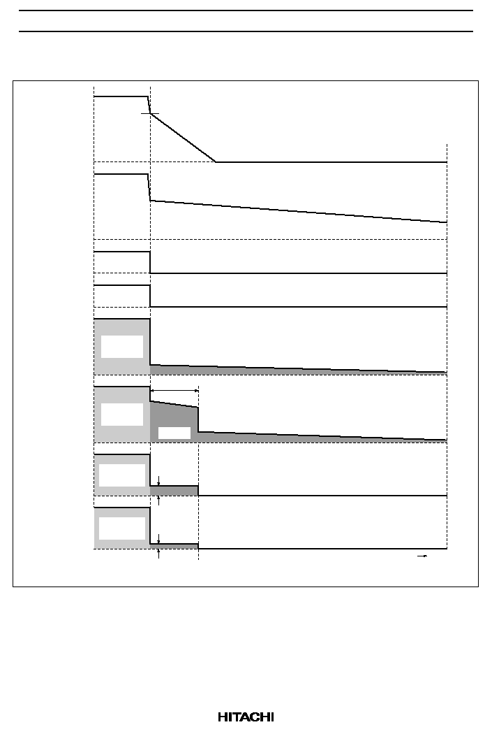
Power Off Retract & Brake
Vpss
Vps
Power
SW
Note: Please see the External Component table about setting delay time t
BRKDLY
.
U
POR
OFF
Braking
ON
GND
GND
Vretsat
t
Vretout
GND
GND
GND
GND
GND
V, W
VCMP
VCMN
Cut off
t
BRKDLY
*
Normal
operation
Normal
operation
Retract off
VCM on
Retract off
VCM on
Figure 7 Operation of Power Off Retract & Brake

HA13614FH
13
Start-up of the Spindle motor
Low
0
0
0
IW
IV
IU
PHASE
COMM
SPNENAB
EXTCOM
EXTCOM
PHASE
COMM
SPNENAB
0
0
0
IW
IV
IU
∑
Not using external commutation mode
∑
Using external commutation mode
Note: "Synchronous driving" is defined as the period after changing SPNENAB = L to H until
the first positive edge of the PHASE signal.
Synchronous driving*
B-EMF sensing driving
Synchronous driving*
B-EMF sensing driving
Figure 8 Start-up of the Spindle Motor

HA13614FH
14
Commutation Timing of the Spindle motor
B-EMF
PHASE
(EXTCOM=1)
PHASE
(EXTCOM=0)
*1
tspndly
*2
*3
tsrctl
commutation
time
U
V
W
Note: 1.
2.
3.
OUTPUT
IU
CT
Vpss
Vpss/2
GND
0
B-EMF
PWM
PWM
PWM
In the case of external commutation mode (EXTCOM=1), the signal PHASE will toggle at every B-
EMF zero-crossing, and selected the internal commutation mode (EXTCOM=0), the PHASE will
have the same period as B-EMF of the spindle motor.
This is delay time by pre-LPF of the B-EMF amplifier. This delay time can be adjust by the value
of external filter capacitor C101, C102. To get the maximum driving efficiency of the spindle
motor, these capacitor value should be chosen as equation (17) in the "External components"
section.
The slew rate of every commutation timing is controllable by changing the SRCTL1, SRCTL2 and
SRCTL3 in the serial port.
Figure 9 Commutation Timing of the Spindle motor
HA13614FH
15
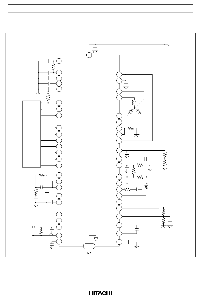
Application
MPU
BRK
BRKDLY
VpsOUT
UFLT
NFLT
FLTOUT
C112
VpsIN
C116
C101
12VGOOD
PHASE
SPNCTL
HA13614FH
OP2IN(+)
COMM
OP1IN(
-
)
OP1OUT
Vss
CLK
SCLK
DATA
SEENAB
VIPWMH
VIPWML
C102
C103
VREF
OP2OUT
VCMIN
DACOUT
C3
to MPU
Vss
(+5V)
Vps
(+12V)
Vss
Vdd
(+3.3V)
POR
C104
C113
R103
R106
R105
C1
C2
C105
DELAY
C110
C111
C114
R2
R3
R101
R110
R109
R102
R107
R108
C117
R
L
TAB
Vpss
CT
U
V
W
RNF
ISENSE
RETPOW
Vpsv
C115
VCMSLC
RETSET
LVI2
VCMP
VCMPS
PC
VCMN
Rs
LVI1
BC1
BC2
VBST
RNF
R
S
C109
C107
R104 C108
C106
19
31
30
23
29
41
35
34
36
37
38
40
39
43
42
3
5
10
45
44
2
1
4
48
46
18
16
15
24
47
9
8
6
7
11
14
12
17
13
26
22
27
21
20
25
28
33
32

HA13614FH
16
External Components
Parts No.
Recommendation
V a l u e
P u r p o s e
N o t e
R101
--
Set up threshold of power monitor for Vps
1
R102
--
R103
5.6 k
Pull up for POR terminal
R104
--
Gain dumping for VCM driver
5
R105
--
Set up output voltage of retract driver for pin VCMP
6
R106
--
R107
--
Set up threshold of power monitor for Vdd
1
R108
--
R109
--
Set up time constance of delayed brake
12
R110
5.6 k
Pull up for 12VGOOD terminal
R2
--
Filter constant of LPF
3
R3
--
Rnf
0.33
Current sensing for spindle motor
7
R
S
0.47
Current sensing for VCM
4
C101, C102
--
Pre-filter of B-EMF amplifier
10
C103
--
Filter of PWMDAC for current control of spindle motor
9
C104
0.1
µ
F
Filter of internal reference output
C105
0.1
µ
F
Set up delay time of
POR
signal
8
C106
0.22
µ
F
Boost up of power supply
C107
2.2
µ
F
Stabilizing boost up voltage
C108
--
Gain dumping for VCM driver
5
C109
0. 1
µ
F
Stabilizing reference voltage of VCM driver
C110
0.1
µ
F
By passing of power supply
C111
0.1
µ
F
C112
--
Keeping brake function
12
C113
0.1
µ
F
By passing of power supply
C114
0.1
µ
F
C115
--
Stabilizing output voltage of retract driver for pin VCMP
11
C116
--
Set up time constance of delayed brake
12
C117
0.1
µ
F
Stabilizing LVI2 terminal
C1
--
Filter constant of LPF
3
C2
--
C3
--
HA13614FH
17
Notes: 1. The operation threshold voltage of Vps or Vdd is determined by resistor R101, R102 or R107,
R108 as follows.
12VGOOD
(for Vps)
POR
(for Vdd)
Vdwn
Vup
Vps
∑ for Vps
R101
R102
Vup(Vps) = (Vsd1 + Vhys3)
1 +
[V]
Recovery
voltage
(1)
R101
R102
Vdwn(Vps) = Vsd1
1 +
[V]
Cut off
voltage
(2)
where, Vsd1 : Operating voltage of the power monitor [V] (refer to Electrical Charasteristics)
Vhys3 : Hysteresis voltage of the power monitor [V] (refer to Electrical Charasteristics)
∑ for Vdd
R107
R108
Vup(Vdd) = (Vsd1 + Vhys4)
1 +
[V]
Recovery
voltage
(1)'
R107
R108
Vdwn(Vdd) = Vsd1
1 +
[V]
Cut off
voltage
(2)'
where, Vhys4 : Hysteresis voltage of the power monitor [V] (refer to Electrical Charasteristics)
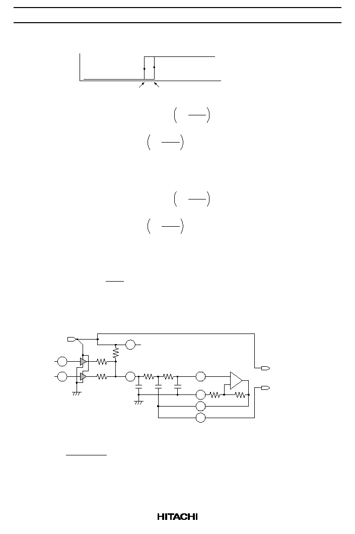
2. The relation between PWMDAC input VIPWMH, VIPWML for VCM driver current control and VCM
driver input (VCMIN ≠ VREF) is determined by following equation. (refer to below figure)
VCMIN
-
VREF =
(64
DPWMH + DPWML)
-
3.2
6.4
6500
(3)
where, VREF
: Internal reference voltage [V] (refer to Electrical Charasteristics)
DPWMH
: Duty of input signal on terminal VIPWMH [%]
DPWML
: Duty of input signal on terminal VIPWML [%]
VREF
VREF
5.3V
R0
VIPWMH
VIPWML
DACOUT
R1L
+
-
C1
VCMIN
to VCM driver
VREF
5.3V
5.3
±
3.2V
R1H
R2
C2
R3
R4
C3
OP2IN(+)
OPAmp.2
GND
OP2OUT
VCMIN
R5
R5/R4=0.604
R1=R1L//R1H//R0
=740
3. The 3rd order LPF at next stage of PWMDAC is characterized by internal OP amp. and capacitor
C1, C2, C3 and resistor R2, R3. These components value are determined by following equations.
C1 =
[F]
1
2
fc
R1
(4)

HA13614FH
18
C3 = 220
10
-
12
[F]
(5)
C2 =
C3
[F]
1
2
4
k + 1
-
8
k + 1
k
2
(6)
R2 =
[
]
k
4
k + 1
-
8
k + 1
2
2
fc
C3
(7)
R3 = R2
[
]
(8)
k =
= 0.604
R5
R4
(9)
where, f c
: Cut off frequency of 3rd order LPF [Hz]
R1
: Output resistance of PWMDAC [
] (refer to Electrical Characteristics)
4. The driving current of VCM Ivcm is determined by following equation.
Ivcm =
Gvcm
[A]
Vvcmin
-
VREF
R
S
(10)
where, Vvcmin : Input voltage on terminal VCMIN (pin 10) [V]
Gvcm
: Transfer function of VCM driver [dB] (refer to Electrical Characteristics)
5. Capacitor C108 and resistor R104 are useful to dump the gain peaking of VCM driver. These
components also determine the gain band width of VCM driver BW1 which should be chosen less
than 10 kHz, as follows.
R104 =
[k
]
12
BW1
Lvcm
R
S
(11)
C108 =
[F]
Lvcm
R
S
+ R
L
1
R104
(12)
where, R
L
: Coil resistance of VCM [
]
Lvcm
: Coil inductance of VCM [H]
6. Retract current Iret is determined by following equation.
R105
R106
0.7
◊
1 +
-
Vretsat
Iret =
[A]
R
S
+ R
L
(13)
Vretsat : Output saturation voltage of retract driver [V]
(refer to Electrical Characteristics)
7. The relation between duty of input signal on terminal SPCNTL (pin 34) and output current of
spindle motor driver Ispn is as follows.
Ispn =
duty
[A]
Vref
-
Voff1
Rnf
(14)
Vref
: Reference voltage of current control amplifier [V]
Vref = Vref2 (@SPNGAIN = 1)
Vref = Vref3 (@SPNGAIN = 0)
Voff1
: Offset voltage of current control amplifier [V]
(refer to Electrical Characteristics)

HA13614FH
19
8. The delay time of the power monitor for start up is as follows.
tpor = 140
C105
[ms]
(15)
9. The cut off frequency fcpwm of the filter for current control input of the spindle motor is as
follows.
fcpwm =
[Hz]
1
2
◊
20k
C103
(16)
10. To get the maximum driving efficiency for spindle motor, the capacitor C101, C102 should be
chosen as following equation.
C101 = 0.8
C102
(17-1)
C102 =
[F]
tan(
/6)
2
13k
1
fbemf
(17-2)
fbemf
: Back EMF frequency at standard rotation speed of the spindle motor [Hz]
where, please set the value of C101, C102 so that C101 < C102 can be kept including the
accuracy of the absolute value to assure the stability of motor starting and speed lock state.
11. To stabilize output voltage od retract driver, the capacitor C115 should be chosen as following
equation. Please chose same values for C115.
C115 =
3
10
-
6
2
(R105 // R106)
[F]
(18)
12. Time t
BRKDLY
of the delayed brake of V, W phase for retract is determined by resistor R109 and
capacitor C112, C116 as following equation.
C116
R109
C116
C112
1 +
t
BRKDLY
=
-
ln 1
-
C116
C112
1 +
Vthb
V
BRK0
[s]
(19)
where, Vthb
: Threshold voltage that output MOS transistor of spindle motor driver is
operated.
V
BRK0
= Vpss ≠ 0.7 [V]
Vpss
: +12 V power supply for spindle motor driver
and, please select capacitor C112 and C116 that the ratio of C112/C116 is more than 3 times,
because the last voltage of BRK and BRKDLY terminals falls if the value of C116 is big for C112,
and effect of brake goes down.
HA13614FH
20
Absolute Maximum Ratings
I t e m
Symbol
Rating
Unit
N o t e
Power supply
Vss
6.0
V
1
Vpss
15
V
2
Vpsv
15
V
2
Spindle current
Ispn
2.0
A
3
VCM current
Ivcm
1.5
A
3
Input voltage
Vin
≠0.33 to Vss +1.0
V
4
Power dissipation
P
T
5.0
W
5
Junction temperature
Tj
150
∞
C
6
Storage temperature
Tstg
≠55 to +125
∞
C
Notes: 1. Operating voltage range is 4.25 V to 5.5 V. If power supply voltage exceed this operating range
in actual application, the reliability of this IC can not be guaranteed.
2. Operating voltage range is 10.2 V to 13.8 V.
3. ASO (Area of Safety Operation) of each output transistor is shown in figure 10.
Operating locus must be within the ASO.
4. Applied to CLK, COMM, SPNCTL, VIPWMH, VIPWML,
SCLK
, DATA and
SEENAB
.
5. Thermal resistance
j-a
30
∞
C/W (Using 4 layer glass epoxy board)
6. Operating junction temperature range is 0
∞
C to +125
∞
C.
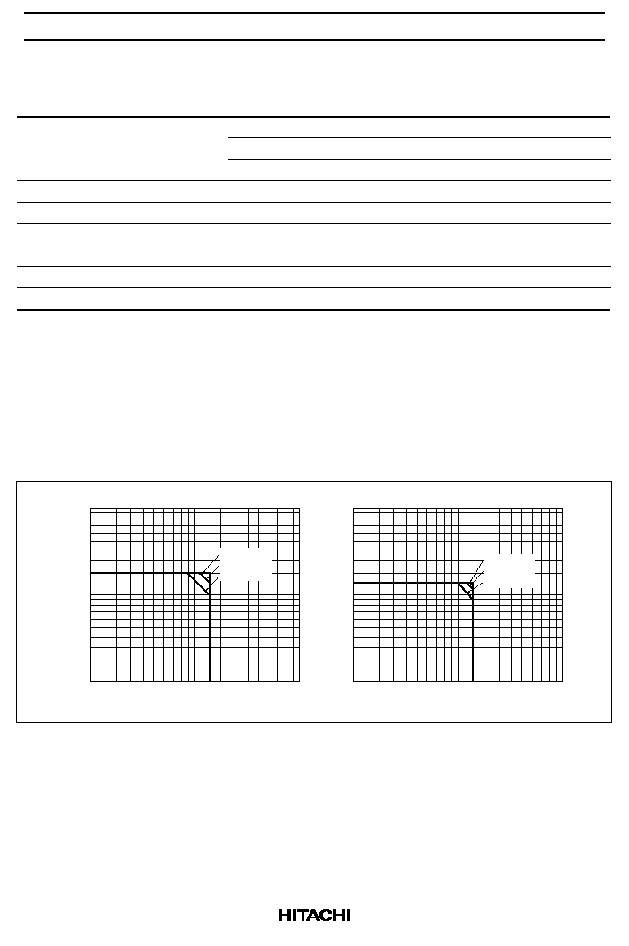
t = 1 ms
t = 10 ms
t = 100 ms
10
0.10
1
10 15
100
1.0
2.0
t = 1 ms
t = 10 ms
t = 100 ms
10
0.10
1
10
VDS (V)
IDS (A)
IDS (A)
VDS (V)
15
100
1.0
1.5
for Spindle motor driver
for VCM driver
Figure 10 ASO of Output Transistor

HA13614FH
21
Electrical Characteristics (Ta = 25
∞
C, Vss = 5 V, Vpss = Vpsv = 12 V)
Item
Symbol
Min
Typ
Max
Unit
Test Conditions
Applicable
Pins
Note
Supply current
Iss0
--
2.0
3.4
mA
Stand by,
fclk=20MHz
Vss
Iss1
--
3.2
4.2
mA
fclk=20MHz
Ips0
--
1.6
2.4
mA
Stand by
Vpss & Vpsv
1
Ips1
--
42
56
mA
Power
switch
Output on
resistance
Ron0
--
0.2
0.3
VpsIN
VpsOUT
Output
leacage
current
Icer0
--
--
±
10
µ
A
VpsOUT=15V,
VpsIN=0V,
Vss=0V,
Vpss=Vpsv=0V
Logic
input
Input low
current
Iil1
--
--
±
10
µ
A
Vil=0V
CLK,
COMM,
Input high
current
Iih1
--
--
±
10
µ
A
Vih1=5V
SCLK
,
DATA,
Input low
voltage
Vil1
--
--
0.8
V
SEENAB
,
VIPWMH,
Input high
voltage
Vih1
2.0
--
--
V
VIPWML,
SPNCTL
Clock
frequency
fclk
19
--
21
MHz
Logic
output1
Output high
voltage
Voh1
4.6
--
--
V
Ioh=1mA
PHASE
Output low
voltage
Vol1
--
--
0.4
V
Iol=2mA
Logic
output2
Output
leakage
current
Icer1
--
--
±
10
µ
A
Vo=5.5V
POR
,
12VGOOD
5
Output low
voltage
Vol2
--
--
0.4
V
Iol=2mA

HA13614FH
22
Electrical Characteristics (Ta = 25
∞
C, Vss = 5 V, Vpss = Vpsv = 12 V) (cont)
Item
Symbol
Min
Typ
Max
Unit
Test Conditions
Applicable
Pins
Note
Spindle
motor
driver
Output on
resistance
Ron1
--
1.2
1.5
Io
1.5A
U, V, W
2
On resistance
during braking
Ron2
--
--
3.0
Io=0.4A,
BRK=3V
Output
leakage
current
Icer3
--
--
±
2
mA
Vo=15V
Output clamp
diode forward
voltage
Vf
--
0.9
1.2
V
If=0.5A
Output MOS
operating
threshold
voltage
Vthb
--
2
--
V
Ron=(Ron/2)
◊
10
Leakage
current on
brake terminal
Icer4
--
--
0.6
µ
A
Vpsv=GND,
Vo=8V
BRK,
BRKDLY
Input filter &
current control
amp.
Vref2
--
490
±
10%
mV
SPNGAIN=1,
SPNCTL=Vss
ISENSE,
FLTOUT
Vref3
--
250
±
10%
mV
SPNGAIN=0,
SPNCTL=Vss
Current
control amp.
offset voltage
Voff1
--
≠10
±
20
mV
SPNCTL=GND
B-EMF
amp.
Input offset
voltage
Voff2
--
--
±
20
mV
Synchronous drive
U, V, W,
UFLT,
NFLT
Voff3
--
--
±
20
mV
B-EMF sens drive
Input
hysteresis
voltage
Vhys1
70
90
110
mVp-p
Synchronous drive
Vhys2
35
45
55
mVp-p
B-EMF sens drive

HA13614FH
23
Electrical Characteristics (Ta = 25
∞
C, Vss = 5 V, Vpss = Vpsv = 12 V) (cont)
Item
Symbol
Min
Typ
Max
Unit
Test Conditions
Applicable
Pins
Note
VCM
driver
Output on
resistance
Ron2
--
1.4
1.8
Io
1.0A
VCMP,
VCMN
2
Output
leakage
current
Icer5
--
--
±
2
mA
Vo=15V
Output
quiescent
voltage
Vq
--
Vpsv/2
±
5%
V
R
S
=0.47
, R
L
=10
,
L=2mH,
R104=1.6M
,
C108=120pF
Transfer gain
Gvcm
--
≠18
--
dB
VCMPS, Rs
4
Gain band
width
BW1
--
10
--
kHz
Input
resistance
Rin
--
60
±
30%
k
VCMIN
PWM
DAC
Input
minimum
pulse width
Tpwm
50
--
--
ns
VIPWMH,
VIPWML
Output
resistance
R1
--
740
±
30%
FLTOUT
Output voltage
Vo1
--
0.4
±
10%
V
VIPWMH=High,
VIPWML=High
VCMPS, Rs
3
Vo2
--
0.4
±
10%
V
VIPWMH=Low,
VIPWML=Low
Output offset
voltage
Voff4
--
--
±
10
mV
Gain ratio
Rat
--
64
±
2%
--
Rat=VIPWMH/
VIPWML
Reference
voltage
Vref
--
5.3
±
5%
V
Io=
±
1mA
VREF
Retract
driver
Retract driver
output voltage
Vretout
--
1.0
±
8%
V
Vpss=6.0V,
R105=13k
,
R106=33k
,
R
L
=10
, R
S
=0.47
VCMP
VCMN output
saturation
voltage
Vretsat
0.1
0.2
0.4
V
VCMN

HA13614FH
24
Electrical Characteristics (Ta = 25
∞
C, Vss = 5 V, Vpss = Vpsv = 12 V) (cont)
Item
Symbol
Min
Typ
Max
Unit
Test Conditions
Applicable
Pins
Note
Power
monitor
Operating
voltage
Vsd1
--
1.415
±
3%
V
LVI1, LVI2
Hysteresis
Vhys3
--
60
--
mV
LVI1
Vhys4
--
30
--
mV
LVI2
Cut off voltage
Vsd2
4.1
--
--
V
Vss
Recovery
voltage
Vrec
--
--
4.4
V
POR delay
time
tpor
10
14
20
ms
C105=0.1
µ
F
POR
OP
amp.1
Output
resistance
Rout2
--
--
10
Shorted between
OP1OUT and
OP1IN(≠)
OP1OUT
Output
maximum
current
Iomax1
--
--
±
1
mA
Output voltage
deviation
Vdev
--
1.415
±
3%
V
Input bias
current
IB1
--
--
±
10
nA
OP1IN(≠)
Gain band
width
BW2
--
1.0
--
MHz
OP1OUT
OTSD
Operating
temperature
Tsd
125
150
--
∞
C
4
Hysteresis
Thys
--
25
--
∞
C
Note:
1. Specified by sum of supply current to Vpss and Vpsv terminal.
2. Specified by sum of saturation voltage and lower saturation voltage.
3. Specified by differential voltage on both side of R
S
at shorting between DACOUT and OP2IN(+),
and between OP2OUT and VCMIN, respectively.
4. Guaranteed by design.
5. The 12VGOOD terminal is open drain output type.

HA13614FH
25
Package Dimensions
36
0
∞
-
8
∞
0.10
0.13 M
17.2
±
0.2
25
37
48
1
12
24
13
17.2
±
0.2
4.85
2.425
0.30
±
0.08
0.65
3.05 Max
1.6
0.8
±
0.3
14
2.7
0.10
±
0.07
0.17
±
0.05
0.825
0.27
±
0.06
0.15
±
0.04
Hitachi Code
JEDEC
EIAJ
Weight (reference value)
FP-48T
1.2 g
Unit: mm
2.925
2.925
4.85
2.425
0.825
2.925
2.925
Dimension including the plating thickness
Base material dimension

Cautions
1. Hitachi neither warrants nor grants licenses of any rights of Hitachi's or any third party's patent,
copyright, trademark, or other intellectual property rights for information contained in this document.
Hitachi bears no responsibility for problems that may arise with third party's rights, including
intellectual property rights, in connection with use of the information contained in this document.
2. Products and product specifications may be subject to change without notice. Confirm that you have
received the latest product standards or specifications before final design, purchase or use.
3. Hitachi makes every attempt to ensure that its products are of high quality and reliability. However,
contact Hitachi's sales office before using the product in an application that demands especially high
quality and reliability or where its failure or malfunction may directly threaten human life or cause risk
of bodily injury, such as aerospace, aeronautics, nuclear power, combustion control, transportation,
traffic, safety equipment or medical equipment for life support.
4. Design your application so that the product is used within the ranges guaranteed by Hitachi particularly
for maximum rating, operating supply voltage range, heat radiation characteristics, installation
conditions and other characteristics. Hitachi bears no responsibility for failure or damage when used
beyond the guaranteed ranges. Even within the guaranteed ranges, consider normally foreseeable
failure rates or failure modes in semiconductor devices and employ systemic measures such as fail-
safes, so that the equipment incorporating Hitachi product does not cause bodily injury, fire or other
consequential damage due to operation of the Hitachi product.
5. This product is not designed to be radiation resistant.
6. No one is permitted to reproduce or duplicate, in any form, the whole or part of this document without
written approval from Hitachi.
7. Contact Hitachi's sales office for any questions regarding this document or Hitachi semiconductor
products.
Hitachi, Ltd.
Semiconductor & Integrated Circuits.
Nippon Bldg., 2-6-2, Ohte-machi, Chiyoda-ku, Tokyo 100-0004, Japan
Tel: Tokyo (03) 3270-2111 Fax: (03) 3270-5109
Copyright ' Hitachi, Ltd., 1999. All rights reserved. Printed in Japan.
Hitachi Asia Pte. Ltd.
16 Collyer Quay #20-00
Hitachi Tower
Singapore 049318
Tel: 535-2100
Fax: 535-1533
URL
NorthAmerica
: http:semiconductor.hitachi.com/
Europe
: http://www.hitachi-eu.com/hel/ecg
Asia (Singapore)
: http://www.has.hitachi.com.sg/grp3/sicd/index.htm
Asia (Taiwan)
: http://www.hitachi.com.tw/E/Product/SICD_Frame.htm
Asia (HongKong)
: http://www.hitachi.com.hk/eng/bo/grp3/index.htm
Japan
: http://www.hitachi.co.jp/Sicd/indx.htm
Hitachi Asia Ltd.
Taipei Branch Office
3F, Hung Kuo Building. No.167,
Tun-Hwa North Road, Taipei (105)
Tel: <886> (2) 2718-3666
Fax: <886> (2) 2718-8180
Hitachi Asia (Hong Kong) Ltd.
Group III (Electronic Components)
7/F., North Tower, World Finance Centre,
Harbour City, Canton Road, Tsim Sha Tsui,
Kowloon, Hong Kong
Tel: <852> (2) 735 9218
Fax: <852> (2) 730 0281
Telex: 40815 HITEC HX
Hitachi Europe Ltd.
Electronic Components Group.
Whitebrook Park
Lower Cookham Road
Maidenhead
Berkshire SL6 8YA, United Kingdom
Tel: <44> (1628) 585000
Fax: <44> (1628) 778322
Hitachi Europe GmbH
Electronic components Group
Dornacher Straße 3
D-85622 Feldkirchen, Munich
Germany
Tel: <49> (89) 9 9180-0
Fax: <49> (89) 9 29 30 00
Hitachi Semiconductor
(America) Inc.
179 East Tasman Drive,
San Jose,CA 95134
Tel: <1> (408) 433-1990
Fax: <1>(408) 433-0223
For further information write to: