 | –≠–ª–µ–∫—Ç—Ä–æ–Ω–Ω—ã–π –∫–æ–º–ø–æ–Ω–µ–Ω—Ç: HA13631T | –°–∫–∞—á–∞—Ç—å:  PDF PDF  ZIP ZIP |

HA13631T
CD-ROM Combo Driver
ADE-207-320 (Z)
1st Edition
Feb. 2000
Description
The HA13631T is combination of Spindle, Forcus, Tracking, Slide, Tray designed for CD-ROM and have
following functions and features.
Functions
∑
1.5 A spindle driver
∑
0.75 A focus driver
∑
0.75 A tracking driver
∑
1.0 A slide driver
∑
0.75 A tray driver
∑
Over temperature shut down (OTSD)
Features
∑
Corresponds to both of sensor motor and sensorless motor
∑
All direct PWM drive
∑
Low on resistance
∑
Low power dissipation
∑
Small thin surface mount package

HA13631T
2
Pin Arrangement
1
2
3
4
5
6
7
8
9
10
11
12
13
14
15
16
17
18
19
20
21
22
23
24
25
26
27
28
(Top view)
56
55
54
53
52
51
50
49
48
47
46
45
44
43
42
41
40
39
38
37
36
35
34
33
32
31
30
29
ASGND
NC
NC
OP1IN
FCSIN
FCSN
FCSP
VFCS
FCSGND
TRKP
TRKN
TRKIN
OP2IN
VSS
SGND
PWMDC
CT2
CT1
RT
REFIN
VCTL
HW-
HW+
HV-
HV+
HU-
VSPN
ASGND
ASGND
SLDIN
OP3IN
OP4IN
VSLD
TRYIN
SLDP
SLDN
SLDGND
VTRY
TRYP
TRYN
BSTGND
BP1
BP2
VBST
U
RNF
V
W
EXTCOM
FGOUT
COMM
BRKSEL
CE
HB
HU+
ASGND

HA13631T
3
Pin Description
Pin No.
Pin Name
Function
1
ASGND
Actuator small signal GND
2
SLDIN
SLD driver control input
3
OP3IN
Inverted input of OP amp. 3 for SLD driver control
4
OP4IN
Inverted input of OP amp. 4 for TRY driver control
5
VSLD
SLD driver power supply
6
TRYIN
TRY driver control input
7
SLDP
SLD driver P output
8
SLDN
SLD driver N output
9
SLDGND
SLD and TRY driver GND
10
VTRY
TRY driver power supply
11
TRYP
TRY driver P output
12
TRYN
TRY driver N output
13
BSTGND
Booster GND
14
BP1
Booster pumping capacitor connection
15
BP2
Booster pumping capacitor connection
16
VBST
Booster output pin. This circuit generates a voltage about two times of the VSPN
pin.
17
U
U phase output
18
RNF
SPN driver current detection
19
V
V phase output
20
W
W phase output
21
EXTCOM
COMM signal on/off control and FGOUT switching. (Refer to the Timing Chart)
22
FGOUT
FG output (Refer to the Timing Chart) open drain
23
COMM
Start-up clock input pin for sensorless (Refer to the Timing Chart)
24
BRKSEL
To select the brake mode (Refer to the Truth Table)
25
CE
Chip enable (Refer to the Truth Table)
26
HB
Hall bias switch
27
HU+
U-phase Hall +input, and U-phase B-EMF connection pin for sensorless
28
ASGND
Actuator small signal GND
29
ASGND
Actuator small signal GND
30
VSPN
SPN driver power supply
31
HU≠
U-phase Hall ≠input, and center tap connection pin for sensorless
32
HV+
V-phase Hall +input, and V-phase B-EMF connection pin for sensorless
33
HV≠
V-phase Hall ≠input, and center tap connection pin for sensorless

HA13631T
4
Pin Description (cont)
Pin No.
Pin Name
Function
34
HW+
W-phase Hall +input, and W-phase B-EMF connection pin for sensorless
35
HW≠
W-phase Hall ≠input, and center tap connection pin for sensorless
36
VCTL
SPN driver control input
37
REFIN
Reference voltage for control inputs. Common to all drivers.
38
RT
Reference voltage. The IC's internal reference current is determined by this
voltage and the external resistor Rt.
39
CT1
Time constant for clock oscillation. The oscillator frequency is determined by the
external capacitor and resistor Ct1 and Rt.
40
CT2
Time constant for PWM carrier. The amplitude is determined by the value of the
external capacitor Ct1.
41
PWMDC
Phase compensation connection pin for matching PWM carrier DC level with
REFIN
42
SGND
SPN small signal GND
43
VSS
Control block power supply. 5 V
44
OP2IN
Inverted input of OP amp. 2 for TRK driver control
45
TRKIN
TRK driver control input
46
TRKN
TRK driver N output
47
TRKP
TRK driver P output
48
FCSGND
FCS and TRK driver GND
49
VFCS
FCS driver power supply
50
FCSP
FCS driver P output
51
FCSN
FCS driver N output
52
FCSN
FCS driver control input
53
OP1IN
Inverted input of OP amp. 1 for FCS driver control
54
NC
No connection
55
NC
No connection
56
ASGND
Actuator small signal GND
HA13631T
5
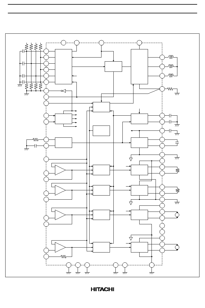
Block Diagram
27
CT
31
32
33
34
35
26
23
COMM
CLK
36
VCTL
24
BRKSEL
25
41
40
CE
37
REFIN
53
OP1IN
Rt
Ct1
W
V
U
Zero cross
detection
1.5 A
SPN
output
22
FGOUT
21
19
20
17
V
W
U
EXTCOM
30
VSPN
43
VSS
ENABLE
15
14
38
39
CLK
OSC
CLK
OP1
PWM
control
PWM
carrier
Vref
C104
Rnf
OTSD
Bias
Logic
FCS
SPN
TRK
SLD
TRY
16
13
49
48
54
55
C103
C103
BP2
BP1
VFCS
50
51
FCS
Vbst
Vbst
Ct2
P
N
PWM
control
47
46
TRK
Vbst
P
N
PWM
control
52
FCSIN
-
+
3
OP3IN
OP3
5
VSLD
7
8
SLD
Vbst
P
N
PWM
control
2
SLDIN
-
+
44
OP2IN
OP2
45
TRKIN
-
+
18
M
4
OP4IN
OP4
10
VTRY
11
12
TRY
Vbst
P
N
PWM
control
6
TRYIN
SGND
-
+
M
9
42
1
28
29
56
5 k

HA13631T
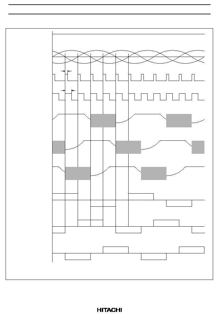
6
Timing Chart
1. Start-up
EN
COMM
Output voltage
(U phase)
FGOUT
Notes: 1.
2.
T1 to T10, and Tmext are set by CPU.
B-EMF sensing is masked while COMM = H.
Also, when EXTCOM = H, B-EMF sensing is masked during the period from T1 to T6.
T1 T3
T5
T6
T2
T4
T7
T8
T9
T10
Vspn
0
Tmext
L
H
EXTCOM
L
H
L
H
Output voltage
(V phase)
Vspn
0
0
Output voltage
(W phase)
Vspn
Output current
(U phase)
0
+
-
0
Output current
(V phase)
+
-
L
H
Mute
(B-EMF detection)
PWM
PWM
PWM
PWM
PWM
0
Output current
(W phase)
+
-
HA13631T
7
2. Acceleration
Output voltage
(U phase)
Note: 1.
Vspn
Reverse start-up
voltage
B-EMF
0
EXTCOM
L
H
Output voltage
(V phase)
Vspn
0
0
Output voltage
(W phase)
Vspn
Output current
(U phase)
0
+
-
0
U
V
W
+
-
0
Output current
(V phase)
+
-
Tmext
Tmint
FGOUT
L
H
0
Output current
(W phase)
+
-
COMM
L
H
PWM
PWM
PWM
PWM
PWM
PWM
PWM
B-EMF sensing is masked while COMM = H (= Tmext) or FGOUT = H (= Tmint).
Tmext is set by the CPU.

HA13631T
8
3. Running
Output voltage
(U phase)
Vspn
Reverse start-up
voltage
B-EMF
0
EXTCOM
L
H
Output voltage
(V phase)
Vspn
0
0
Output voltage
(W phase)
Vspn
Output current
(U phase)
0
+
-
0
U
V
W
+
-
0
Output current
(V phase)
+
-
FGOUT
0
Output current
(W phase)
+
-
L
H
Zero cross
detection
input
0
U
V
W
+
-
PWM
PWM
PWM
PWM
PWM
PWM
Td
Notes: 1.
2.
Delay time Td is determined by C105 to C107, and R109 to R116.
Refer to the section of External Components.
B-EMF sensing is masked while FGOUT = H (= Tmint). The Tmint time is set internally.
Refer to the Electrical Characteristics.

HA13631T
9
Truth Table
Table 1
CE and BRKSEL
CE
BRKSEL
SPN Driver
FCS Driver
TRK Driver
SLD Driver
TRY Driver
L
L
Z
Z
Z
Z
Z
H
Enable *
2
Enable
Enable
Z
Enable
H
L
Enable *
3
Enable
Enable
Enable
Z
H
Enable *
2
Enable
Enable
Enable
Z
Notes: 1. Z: Hi impedance
2. Short brake mode
3. Reverse brake mode
Table 2
EXTCOM and COMM
EXTCOM
COMM
T1~T6
Mask
T7~
Mask
FGOUT
(@P = 12)
Logic
L
L
OFF
Internal
6 cycle/rotation
Corresponds to sensor
H
OFF
Internal
Corresponds to sensorless
H
L
ON
Internal
36 pulse/rotation
H
ON
External

HA13631T
10
Application
VSPN
VSS
HUN
HVP
HVN
HWP
HB
COMM
FGOUT
EXTCOM
VCTL
REFIN
BRKSEL
CE
RT
CT1
C105a~d
R101a~d
HUP
W
B1
B2
U
V
+5 V or
+12 V
+5 V or
+12 V
+5 V or
+12 V
FCS
+5 V
TRYIN
OP4IN
MPU
DSP
HWN
Ct1
C101
C103
RNF
Rnf
VBST
VFCS
+5 V or
+12 V
VSLD
VTRY
FCSP
FCSN
TRYP
TRYN
BSTGND
FCSGND
P55
P54
SLDGND
SGND
ASGND
C102
C104
PWMDC
Ct2
CT2
TRY
R110
R109
R102a~d
SLDIN
OP3IN
R108
R107
TRKIN
OP2IN
R106
R105
FCSIN
OP1IN
R104
R103
Rt
M
SLDP
SLDN
SLD
M
TRK
TRKP
TRKN
HA13631T
11
External Components
Parts No.
Reccomended
Value
Reccomended
Range
Purpose
Note
R101a~d
2.4 k
22 k
Filter resistor and atenuation for B-EMF
1
R102a~d
7.5 k
22 k
Filter resistor and atenuation for B-EMF
1
R103, R104
--
220 k
for FCS driver gain setting
R105, R106
--
220 k
for TRK driver gain setting
R107, R108
--
220 k
for SLD driver gain setting
R109, R110
--
220 k
for TRY driver gain setting
5
Rnf
0.25
0.25
SPN driver current detection resistor
2
Rt
6.8 k
5 k
Reference current setting
C101
--
0.1
µ
F
for Power supply by passing
C102
0.1
µ
F
--
for Booster pumping
C103
0.47
µ
F
--
for Booster output smoothing
C104
2200 pF
--
for PWM carrier oscillation DC level adjustment
C105a~d
0.1
µ
F
--
for B-EMF filter
1
Ct1
100 pF
--
Time constant for CLK oscillation
3, 4
Ct2
400 pF
--
PWM carrier generation time constant
3, 4
Notes: 1. The values of R101a~d, R102a~d, and C105a~d are determined by the following equation.
Where, Nomax : Maximum rotation speed (rpm)
P
: Number of spindle motor poles (Total number of S poles and N poles)
R101
R102
1
4
(at Vspn = 5 V)
11
Nomax P
1
R101x
1
R102x
C105x =
+
2. The output current maximum value Iospnmax of SPN driver is controlled according to the
following equation. However, Vspncl is the current limiter reference voltage. (See the electrical
characteristics)
Iospnmax =
Vspncl
Rnf
3. The CLK oscillation frequency fclk and Rt1
Ct1 are related by the following equation.
Vrt
2 Ct1 Rt (Vct1h
-
Vct1l)
fclk =
fclk =
Where, Vrt
: RT pin voltage (See the electrical characteristics)
Vct1h : CT1 pin high voltage (See the electrical characteristics)
Vct1l : CT1 pin low voltage (See the electrical characteristics)

HA13631T
12
4. The PWM carrier frequency fpwm and the amplitude Apwm are determined by the following
equation.
fpwm =
Vrt
8 Ct1 Rt (Vct1h
-
Vct1l)
Apwm =
(Vct1h
-
Vct1l)
4 Ct1
Ct2
However, Ct2 = 4 Ct1
5. As 5 k
appears as an internal resistance at TRYIN (pin 6), caution is required when marking
the gain setting.

HA13631T
13
Absolute Maximum Ratings (Ta = 25
∞
C)
Item
Symbol
Rating
Unit
Note
Control block supply voltage
Vss
7
V
1
SPN supply voltage
Vspn
7
V
1
FCS & TRK supply voltage
Vfcs
9.5
V
1
SLD supply voltage
Vsld
7
V
1
TRY supply voltage
Vtry
9.5
V
1
Input voltage
Vin
0 to Vss
V
2
SPN output current
Iospn
1.5 (2.5)
A
3
FCS output current
Iofcs
0.75 (1.5)
A
3
TRK output current
Iotrk
0.75 (1.5)
A
3
SLD output current
Iosld
1.0 (1.5)
A
3
TRY output current
Iotry
0.75 (1.5)
A
3
Power dissipation
Pt
2.5
W
4
Junction temperature
Tj
150
∞
C
1
Storage temperature range
Tstg
≠55 to +125
∞
C
Note:
1. Operating range is shown below.
Vss = 4.5 to 5.5 V, Vspn = 4.25 to 5.75 V, Vfcs = 4.25 to 8.5 V, Vsld = 4.25 to 5.75 V, Vtry = 4.25
to 8.5 V, Tjopr = ≠20 to +135
∞
C
When operating with Vfcs > Vss, it is necessary to set Vtry = Vfcs. Also, settings must be made
that satisfy the following condition:
Vtry + Vss ≠ Vsld
8.5 V
2. Applied to analog and logic input.
3. Values in parentheses are peak values. ASO (Area of Safety Operation) is shown below.
Drain Current Id (A)
ASO of SPN Driver
0.1
3
1
0.5
The voltage between Drain and Source Vds (V)
1.5
0.2
0.3
2
2.5
20
1
5
10 15
2
3
Drain Current Id (A)
ASO of SLD Driver
0.1
3
1
0.5
The voltage between Drain and Source Vds (V)
1.5
0.2
0.3
2
20
1
5
10 15
2
3
Drain Current Id (A)
ASO of FCS
TRK
TRY Driver
0.1
3
1
0.5
The voltage between Drain and Source Vds (V)
1.5
0.2
0.3
2
20
1
5
10 15
2
3
t = 0.1 ms
Duty = 1/3
Duty = 1/2
Duty = 1/2
t = 10 ms
t = 1 ms
t = 1 ms
t = 0.1 ms
t = 0.1 ms
t = 10 ms
t = 10 ms
t = 1 ms
4. Thermal resistance is shown below.
j-tab
6
∞
C/W (back side tab soldering area is 70% or more)
j-a1
30
∞
C/W (mounted on 4 layer glass-epoxy board, back side tab soldering area is 70% or
more)

HA13631T
14
Electrical Characteristics
(Ta = 25
∞
C, Vss = 5 V, Vspn = 12 V, Vfcs = 5 V, Vsld = 12 V)
Item
Symbol
Min
Typ
Max
Unit
Test Conditions
Applicable
Pins
Note
Quiescent current
Iss0
--
0.2
0.5
mA
CE = L
VSS
Ispn0
--
0.1
0.2
mA
VSPN
Ifcs0
--
--
0.1
mA
VFCS
Isld0
--
--
0.1
mA
VSLD
Itry0
--
--
0.1
mA
VTRY
Iss1
--
25
35
mA
CE = H
VSS
Ispn1
--
--
1.0
mA
All load open
VSPN
Ifcs1
--
--
1.0
mA
VFCS
Isld1
--
--
1.0
mA
VSLD
Itry1
--
4.0
6.0
mA
VTRY
Logic
Input current
Iin
--
--
±
10
µ
A
Vin = 0 to Vss
EXTCOM,
input
Low level voltage
Vil
--
--
0.8
V
COMM,
High level voltage
Vih
2.0
--
--
V
BRKSEL,
CE
Logic
Low level voltage
Vol
--
0.2
0.4
V
Io = 1 mA
FGOUT
output 1
Leakage current
I
CER
1
--
--
±
10
µ
A
V
CE
= 5.5 V
Logic
Low level voltage
Vol
--
0.3
0.6
V
Io = 15 mA
HB
output 2
Leakage current
I
CER
1
--
1.2
1.5
µ
A
V
CE
= 5.5 V
SPN
driver
Output on
resistance
Ronspn
--
1.2
1.5
Io = 1.0 A
U, V, W
1
Leakage current
Ioffspn
--
--
±
100
µ
A
Vspn = 15 V
Slew rate
SRspn
--
60
--
V/
µ
s
Load open
5
Current limiter
voltage
Vspncl
--
0.25
±
10%
V
Rnf = 0.25
RNF
FCS/
TRK
Output on
resistance
Ronfcs
--
3.0
3.75
Io = 0.5 A
FCSP/N,
TRKP/N
1
driver
Leakage current
Iofffcs
--
--
±
100
µ
A
Vfcs = 15 V
Slew rate
SRfcs
--
60
--
V/
µ
s
Load open
5
SLD
driver
Output on
resistance
Ronsld
--
2.0
2.5
Io = 1.0 A
SLDP/N
1
Leakage current
Ioffsld
--
--
±
100
µ
A
Vsld = 15 V
Slew rate
SRsld
--
60
--
V/
µ
s
Load open
5

HA13631T
15
Electrical Characteristics
(Ta = 25
∞
C, Vss = 5 V, Vspn = 12 V, Vfcs = 5 V, Vsld = 12 V) (cont)
Item
Symbol
Min
Typ
Max
Unit
Test Conditions
Applicable
Pins
Note
TRY
driver
Output on
resistance
Rontry
--
3.0
3.75
Io = 0.5 A
TRYP/N
1
Leakage current
Iofftry
--
--
±
100
µ
A
Vtry = 15 V
Slew rate
SRtry
--
125
--
V/
µ
s
Load open
5
CLK
RT voltage
Vrt
--
1.37
±
5%
V
RT
OSC
CT1 charge current
Ict1p
--
180
±
10%
µ
A
Rt = 6.8 k
CT1
CT1 discharge
current
Ict1n
--
≠180
±
10%
µ
A
Rt = 6.8 k
CT1 high voltage
Vct1h
--
2.7
±
0.1
V
CT1 low voltage
Vct1l
--
1.47
±
0.1
V
CLK oscillation
frequency
fclk
--
460
±
10%
kHz
Ct1 = 100 pF
Bias
Drive frequency
fbst
--
fclk/2
--
kHz
BP1
Output voltage
Vbst
16.0
16.5
--
V
Vspn = 12 V
VBST
9.0
9.5
--
V
Vspn = 5 V
PWM
PWM frequency
fpwm
--
fclk/4
--
kHz
CT2
carrier
CT2 charge current
Ict2p
--
180
±
10%
µ
A
Rt = 6.8 k
CT2 discharge
current
Ict2n
--
≠180
±
10%
µ
A
Rt = 6.8 k
DC feedback
resistance
Rdc
--
20
±
20%
k
PWMDC
Offset voltage
Vospwm
--
--
±
30
mV
Zero
cross
Common mode
input voltage range
Vczd
0
--
4.0
V
HU+/≠,
HV+/≠,
detection
Input voltage range
Vinzd
50
--
--
mVpp
HW+/≠
Hysteresis
Vhyszd
11
16
21
mVpp
FGOUT pulse
width
Tmint
--
64/
fclk
±
4/
fclk
µ
s
FGOUT
SPN
Input current
Ictl
--
--
±
3.0
µ
A
Vctl = 0.5 to 4.5 V
VCTL
control
Dead zone voltage
Vdzctl
±
50
--
±
200
mV
2
REFIN voltage
range
Vref
1.0
--
2.65
V
REFIN
4
Control gain
Dspn
119
139
159
%/V
Ct2 = 680 pF,
Ct1 = 100 pF
U, V, W
2

HA13631T
16
Electrical Characteristics
(Ta = 25
∞
C, Vss = 5 V, Vspn = 12 V, Vfcs = 5 V, Vsld = 12 V) (cont)
Item
Symbol
Min
Typ
Max
Unit
Test Conditions
Applicable
Pins
Note
OP1~
Input current
Iinop
--
--
±
0.1
µ
A
Vin = 0 to Vss
OP1~4IN
OP4
Offset voltage
Vosop
--
--
±
60
mV
FCSIN,
Open loop gain
Gvolop
--
64
--
dB
f = 1kHz
TRKIN,
5
Gain bandwidth
Bop
--
1.6
--
MHz
SLDIN,
TRYIN
5
OP1~
OP3
Output low
voltage
Voopl
--
--
0.5
V
Io = ≠0.2 mA
FCSIN,
TRKIN,
Output high
voltage
Vooph
Vss
≠1.0
--
--
V
Io = 0.2 mA
SLDIN
OP4
Output low
voltage
Voopl
--
--
0.5
V
Io = ≠0.03 mA
TRYIN
Output high
voltage
Vooph
Vss
≠1.7
--
--
V
Io = 0.03 mA
FCS/
TRK/
Quiescent offset duty
Dqfcs
--
--
±
2
%
FCS/TRK/SLD/
TRYIN = REFIN
FCSP/N,
TRKP/N,
3
SLD/
TRY
control
Control gain
Dfcs
63
68
73
%/V
Ct2 = 680 pF,
Ct1 = 100 pF
SLDP/N,
TRYP/N
OTSD
Operating temperature
Tsd
135
180
--
∞
C
5
Hysteresis
Thys
--
80
--
∞
C

HA13631T
17
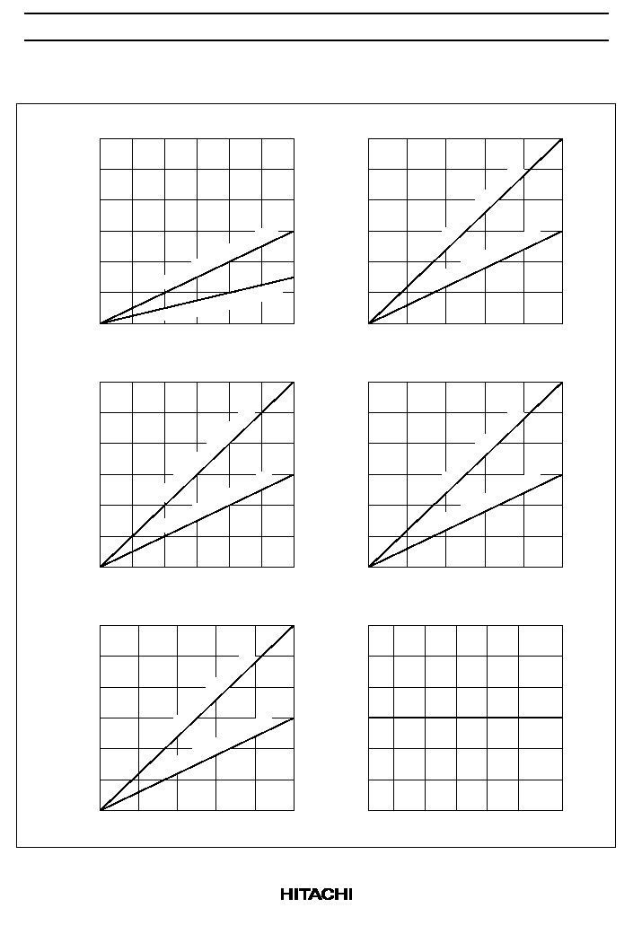
Note:
1. Specified by sum of the upper and lower saturation voltages.
2. See figure 1. Where,
Dspn =
D
Vctl
Reverse
torque
Forward
torque
Vctl(V)
Vdzctl
D
Vctl
Vref
0
100
Duty
(%)
Figure 1
3. See figure 2. Where, x = fcs, trk, sld, try.
Dx =
D
Vxin
Vref
Vxin
N
P
D
Vxin
0
100
50
X = fcs, trk, sld, try
Duty
(%)
Figure 2
4. If Vref < 1.5 V, 100% PWM duty control may not be possible.
5. Design guide only.
HA13631T
18
Reference Data
Output Current Iospn (A)
1.0
0.5
0
1.5
3
1
2
0
Output Saturation Voltage Vsatspn (V)
SPN Driver Output Saturation Voltage vs.
Output Current
FCS Driver Output Saturation Voltage vs.
Output Current
Output Current Iofcs (A)
Output Saturation Voltage Vsatfcs (V)
0.6
0.4
0.8
0.2
0
1.0
3
1
2
0
Output Current Iosld (A)
1.0
0.5
0
1.5
Output Saturation Voltage Vsatsld (V)
SLD Driver Output Saturation Voltage vs.
Output Current
TRK Driver Output Saturation Voltage vs.
Output Current
Output Current Iotrk (A)
Output Saturation Voltage Vsattrr (V)
3
1
2
0
Output Current Iotry (A)
0
3
1
2
0
Output Saturation Voltage Vsattry (V)
TRY Driver Output Saturation Voltage vs.
Output Current
RT Voltage vs. Junction Temperature
Junction Temperature Tj (
∞
C)
RT Voltage Vrt (V)
1.6
1.2
1.4
1.0
-
20
100
75
50
25
0
135
3
1
2
0
0.6
0.4
0.8
0.2
0
1.0
0.6
0.4
0.8
0.2
1.0
Upper arm, Lower arm
Upper arm, Lower arm
Upper arm + Lower arm
Upper arm, Lower arm
Upper arm + Lower arm
Upper arm, Lower arm
Upper arm + Lower arm
Upper arm, Lower arm
Upper arm + Lower arm
Upper arm + Lower arm

HA13631T
19
Package Dimensions
Hitachi Code
JEDEC
EIAJ
Weight (reference value)
TTP-56DT
--
--
0.32 g
Unit: mm
*Dimension including the plating thickness
Base material dimension
0.08
M
0.10
*0.17
±
0.05
8.10
±
0.20
0.65 Max
1
28
29
56
14.0
6.10
0
∞
≠ 8
∞
0.50
1.20 Max
0.05
±
0.05
14.2 Max
0.15
±
0.04
0.50
±
0.1
1.0
*0.21
+0.04
≠0.05
0.19
+0.03
≠0.05
56
29
28
1
(9.30)
(3.50)
(2.50)
(7.20)
HA13631T
20
Cautions
1. Hitachi neither warrants nor grants licenses of any rights of Hitachi's or any third party's patent,
copyright, trademark, or other intellectual property rights for information contained in this document.
Hitachi bears no responsibility for problems that may arise with third party's rights, including
intellectual property rights, in connection with use of the information contained in this document.
2. Products and product specifications may be subject to change without notice. Confirm that you have
received the latest product standards or specifications before final design, purchase or use.
3. Hitachi makes every attempt to ensure that its products are of high quality and reliability. However,
contact Hitachi's sales office before using the product in an application that demands especially high
quality and reliability or where its failure or malfunction may directly threaten human life or cause risk
of bodily injury, such as aerospace, aeronautics, nuclear power, combustion control, transportation,
traffic, safety equipment or medical equipment for life support.
4. Design your application so that the product is used within the ranges guaranteed by Hitachi particularly
for maximum rating, operating supply voltage range, heat radiation characteristics, installation
conditions and other characteristics. Hitachi bears no responsibility for failure or damage when used
beyond the guaranteed ranges. Even within the guaranteed ranges, consider normally foreseeable
failure rates or failure modes in semiconductor devices and employ systemic measures such as fail-
safes, so that the equipment incorporating Hitachi product does not cause bodily injury, fire or other
consequential damage due to operation of the Hitachi product.
5. This product is not designed to be radiation resistant.
6. No one is permitted to reproduce or duplicate, in any form, the whole or part of this document without
written approval from Hitachi.
7. Contact Hitachi's sales office for any questions regarding this document or Hitachi semiconductor
products.
Hitachi, Ltd.
Semiconductor & Integrated Circuits.
Nippon Bldg., 2-6-2, Ohte-machi, Chiyoda-ku, Tokyo 100-0004, Japan
Tel: Tokyo (03) 3270-2111 Fax: (03) 3270-5109
Copyright ' Hitachi, Ltd., 2000. All rights reserved. Printed in Japan.
Hitachi Asia Pte. Ltd.
16 Collyer Quay #20-00
Hitachi Tower
Singapore 049318
Tel: 535-2100
Fax: 535-1533
URL
NorthAmerica
: http:semiconductor.hitachi.com/
Europe
: http://www.hitachi-eu.com/hel/ecg
Asia (Singapore)
: http://www.has.hitachi.com.sg/grp3/sicd/index.htm
Asia (Taiwan)
: http://www.hitachi.com.tw/E/Product/SICD_Frame.htm
Asia (HongKong)
: http://www.hitachi.com.hk/eng/bo/grp3/index.htm
Japan
: http://www.hitachi.co.jp/Sicd/indx.htm
Hitachi Asia Ltd.
Taipei Branch Office
3F, Hung Kuo Building. No.167,
Tun-Hwa North Road, Taipei (105)
Tel: <886> (2) 2718-3666
Fax: <886> (2) 2718-8180
Hitachi Asia (Hong Kong) Ltd.
Group III (Electronic Components)
7/F., North Tower, World Finance Centre,
Harbour City, Canton Road, Tsim Sha Tsui,
Kowloon, Hong Kong
Tel: <852> (2) 735 9218
Fax: <852> (2) 730 0281
Telex: 40815 HITEC HX
Hitachi Europe Ltd.
Electronic Components Group.
Whitebrook Park
Lower Cookham Road
Maidenhead
Berkshire SL6 8YA, United Kingdom
Tel: <44> (1628) 585000
Fax: <44> (1628) 778322
Hitachi Europe GmbH
Electronic components Group
Dornacher Stra
e 3
D-85622 Feldkirchen, Munich
Germany
Tel: <49> (89) 9 9180-0
Fax: <49> (89) 9 29 30 00
Hitachi Semiconductor
(America) Inc.
179 East Tasman Drive,
San Jose,CA 95134
Tel: <1> (408) 433-1990
Fax: <1>(408) 433-0223
For further information write to: