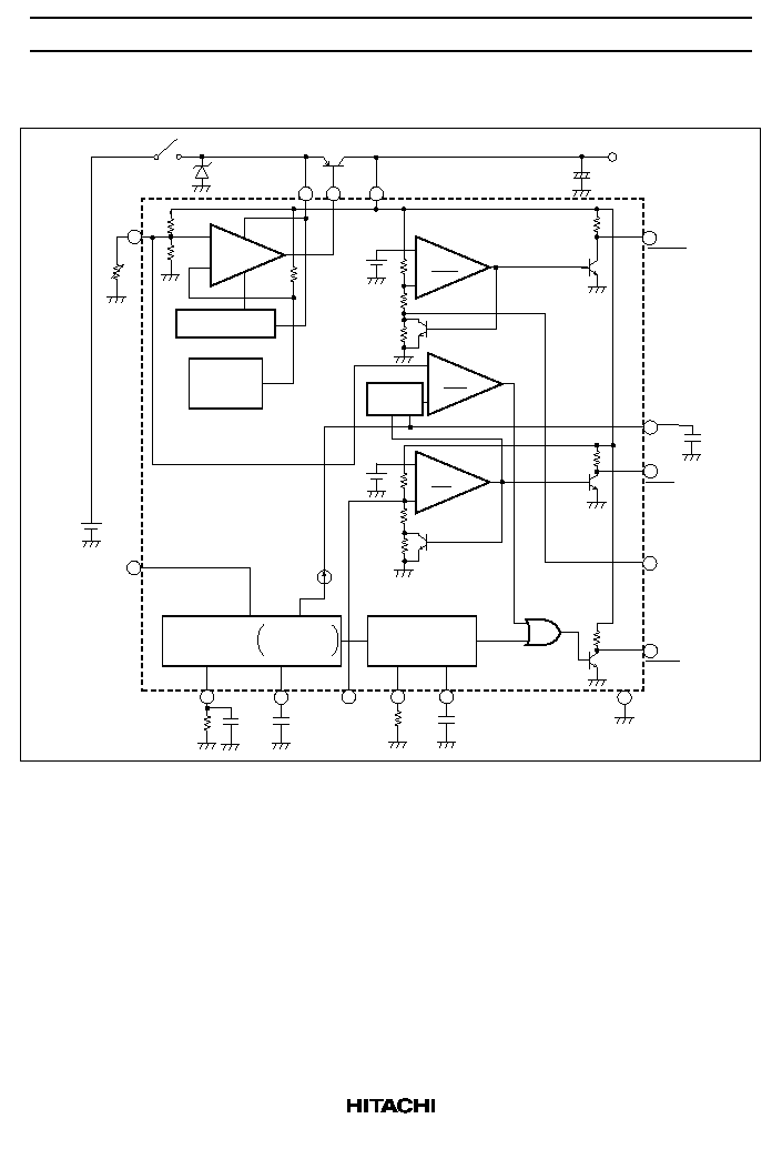
HA16103 FPJ/FPK
Watchdog Timer
Description
The HA16103FPJ/FPK monolithic voltage control is designed for microcomputer systems. In addition to
voltage regulator, it includes watch dog timer function, power on reset function, and output voltage monitor
function.
It is suitable for battery use microcomputer systems.
Functions
∑
5 V regulated power supply
∑
Power on reset pulse generator
∑
Watch dog timer
∑
Low voltage inhibit protection
Features
∑
Wide operational supply voltage range (V
CC
= 6 to 40 V)
∑
Various control signals are generated when microcomputer system runaway occurs. (
NMI signal and
STBY signal are generated by detecting voltage level, and RES signal is generated by monitoring the
time after
NMI signal is detected)
∑
Regulated voltage,
NMI detecting voltage, STBY detecting voltage are adjustable.
∑
At low voltage and re-start, the delay time of
RES signal is adjustable
∑
Watchdog timer filtering uses the minimum clock input pulse width and maximum cycle detection
method
Ordering Information
Type No.
Package
HA16103FPJ
FP-20DA
HA16103FPK
FP-20DA

HA16103 FPJ/FPK
3
Pin Functions
No.
Pin Name
Description
1
NC
NC pin
2
P-RUN
P-RUN signal input pin for watchdog timer
3
Rf
Connect resistor Rf. Frequency bandwidth of the filter circuit depends on Rf
4
Cf
Connect resistor Cf. Frequency bandwidth of the filter circuit depends on Cf
5
R
R
Connect resistor R
R
. Reset-signal power-on time depends on R
R
6
C
R
Connect resistor C
R
. Reset-signal power-on time depends on C
R
7
GND
Ground
8
Voadj
5-V reference voltage fine-tuning pin. Connect a resistor between this pin and
GND. The value of output voltage is given by
V
OUT
= {1 + 5.34/(R1 // 2.0)}
◊
Voadj Unit for R1: k
9
V
OUT
Connect the collector of an external PNP-type transistor. The pin supplies 5-V
regulated voltage for internal circuit
10
NC
NC pin
11
NC
NC pin
12
V
CONT
The external PNP-type transistor's base control pin
13
V
CC
Supply voltage pin. Operating supply voltage range is 6.0 to 40 V.
14
C
RES
If the voltage of V
OUT
pin declines to less than Detection voltage(1) (because of
an instant power cut or other cause),
NMI
signals are generated.
If t
RES
0.5∑Rf∑C
RES
(sec) has passed since then,
RES
signals are generated.
If the voltage of V
OUT
pin inclines to more than Detection voltage(1) (in case of
re-start from LVI state),
NMI
signals are stop. t
r
0.5∑Rf∑C
RES
(sec) has passed
since then,
RES
signals are stop. Connect capacitor C
RES
between this pin and
GND to adjust the
RES
signals delay time(t
RES
, t
r
). If delay time is unnecessary,
make this pin open (t
RES
= 2
µ
s typ. t
r
= 10
µ
s typ. at open)
15
V
NMIadj
NMI
detection voltage fine-tuning pin. Connect a resistor between this pin and
V
OUT
pin or GND. The value of output voltage is given by
V
NMI
= {1 + (R2 // 25.5)/(R3 // 10.6)}
◊
V
NMIadj
. Unit for R2, R3: k
16
NMI
NMI
signal output pin. Connect to pin
NMI
of the microcomputer
17
RES
RES
signal output pin. Connect to pin
RES
of the microcomputer
18
V
STBYadj
STBY
detection voltage tuning pin. Connect a resistor between this pin and
V
OUT
or GND. The value of output voltage is given by
V
STBY
= 1.89
◊
{1 + 21/(7.9 + 8.85 // R4)}
◊
V
STBYadj
Unit for R4: k
19
STBY
STBY
signal output pin. Connect to pin
STBY
of the microcomputer
20
NC
NC pin

HA16103 FPJ/FPK
5
Functional Description
Stabilized Power Supply Function
The stabilized power supply includes the following features:
∑
Wide range of operating input voltage from 6 V to 40 V to provide stabilized voltages
∑
Availability of any output current, by simply replacing the external transistor
∑
Fine adjustment of output voltage
Figure 1 shows the fine adjustment circuit of the output circuit. Select the resistor R1 as shown in
equation 1.
Add a resistor between GND and Voadj to increase the output voltage.
HA16103
To micro-
computer system
C1
100
µ
F
V
CC
V
GND
V
Q1
BATT
CONT
V
OUT
R
1
Vout = (1+ ) Voadj
Equation 1
5.34
R // 2.0
◊
1
(Voadj 1.31V)
(R
1
: k
)
Figure 1 Fine Adjustment Circuit of Output Voltage
0
5
10
5
4
3
2
1
1 A
(Ta = 25
∞
C)
Input voltage V
CC
(V)
Output voltage (V)
I = 0.1 A
OUT
0.5 A
1 : 1
Figure 2 Output Voltage Characteristic