 | –≠–ª–µ–∫—Ç—Ä–æ–Ω–Ω—ã–π –∫–æ–º–ø–æ–Ω–µ–Ω—Ç: HA16108FP | –°–∫–∞—á–∞—Ç—å:  PDF PDF  ZIP ZIP |

HA16107P/FP, HA16108P/FP
PWM Switching Regulator for
High-performance Voltage Mode Control
Description
The IC products in this series are primary control switching regulator control IC's appropriate for obtaining
stabilized DC voltages from commercial AC power.
These IC's can directly drive power MOS FET's, they have a timer function built in to the secondary
overcurrent protection, and they can perform intermittent operation or delayed latched shutdown as
protection operations in unusual conditions. They can be used to implement switching power supplies with
a high level of safety due to the wide range of built-in functionality.
Functions
∑
6.45 V reference voltage
∑
Triangle wave generator
∑
Error amplifier
∑
Under voltage lockout protector
∑
PWM comparator
∑
Pulse-by-pulse current limitting
∑
Timer-latch current limitting (HA16107)
∑
ON/OFF timer function (HA16108)
∑
Soft start and quick shutdown
∑
Output circuit for power MOS FET driving

HA16107P/FP, HA16108P/FP
2
Features
∑
Operating frequencies up to a high 600 kHz
∑
Built-in pre-driver circuit for driving power MOS FET
∑
Built-in timer latch over-current protection function (HA16107)
∑
The OCL enables intermittent operation by an ON/OFF timer for prevention of secondary overcurrent.
(HA16108)
∑
The UVL function (under voltage lockout) is applied to both Vin and Vref.
∑
ON/OFF reset: an auto-reset function which is based on the time constant of an external capacitor and
observation of drops in Vin.
∑
Since the over-voltage protection function OVP (the TL pin) only observes voltage drops in Vin, it is
possible to use the OVP and ON/OFF pin for independent purposes.
∑
Built-in 34 V Zener diode between Vin and ground.
Ordering Information
Typical Threshold Voltage
Product
UVL1
OVP
Notes
Package
HA16107P
Hi: 16.2 V
7.0 V
Timer latch protection
DP-16
HA16107FP
Lo: 9.5 V
FP-16DA
HA16108P
Hi: 16.2 V
Hi: 7.0 V
On-off timer protection
DP-16
HA16108FP
Lo: 9.5 V
Lo: 1.3 V
(intermittent operation possible)
FP-16DA
HA16107P/FP, HA16108P/FP
3
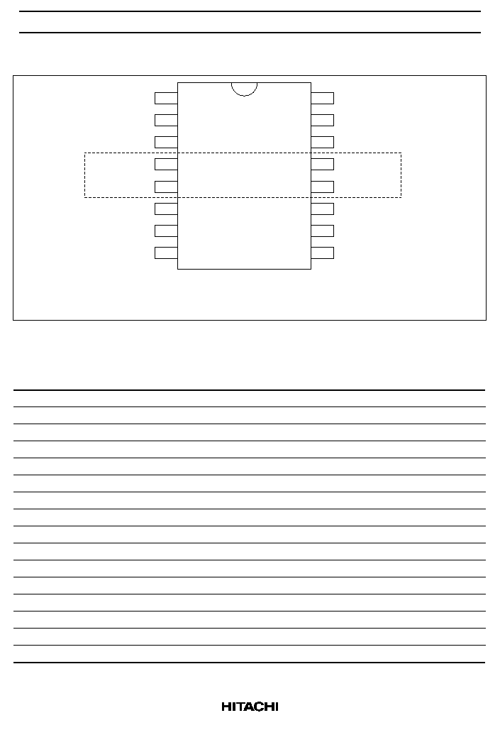
Pin Arrangement
V
IN
OUT
CL(+)
V
E
CL(
-
)
R
T1
C
T
R
T2
TL, ON/OFF
E/O
IN(
-
)
NC
GND
IN(+)
ST
Vref
(Top view)
1
2
3
4
5
6
7
8
16
15
14
13
12
11
10
9
Note 1
Note 2
Notes: 1.
2.
In the SOP package models (HA16107FP and HA16108FP) pins 4, 5, and 13 are connected
inside the IC. However, all must be connected to the system ground.
Pin 16 is TL (HA16107), ON/OFF (HA16108).
Pin Functions
∑
HA16107P, HA16108P
Pin No.
Symbol
Pin Functions
1
V
IN
Input voltage
2
OUT
Pulse output
3
CL (+)
Current limiter
4
V
E
Output ground
5
CL (≠)
Current limiter
6
R
T1
Timing resistor (rising time)
7
C
T
Timing capacitor
8
R
T2
Timing resistor (falling time)
9
Vref
Reference voltage output
10
ST
Soft start
11
IN (+)
Error amp (+) input
12
GND
Ground
13
NC
NC
14
IN (≠)
Error amp (≠) input
15
E/O
Error output
16
TL, ON/OFF
Timer latch (HA16107), ON/OFF (HA16108)

HA16107P/FP, HA16108P/FP
4
∑
HA16107FP, HA16108FP
Pin No.
Symbol
Pin Functions
1
V
IN
Input voltage
2
OUT
Pulse output
3
CL (+)
Current limiter
4
GND
Ground
5
GND
Ground
6
R
T1
Timing resistor (rising time)
7
C
T
Timing capacitor
8
R
T2
Timing resistor (falling time)
9
Vref
Reference voltage output
10
ST
Soft start
11
IN (+)
Error amp (+) input
12
GND
Ground
13
GND
Ground
14
IN (≠)
Error amp (≠) input
15
E/O
Error output
16
TL, ON/OFF
Timer latch (HA16107), ON/OFF (HA16108)
HA16107P/FP, HA16108P/FP
5
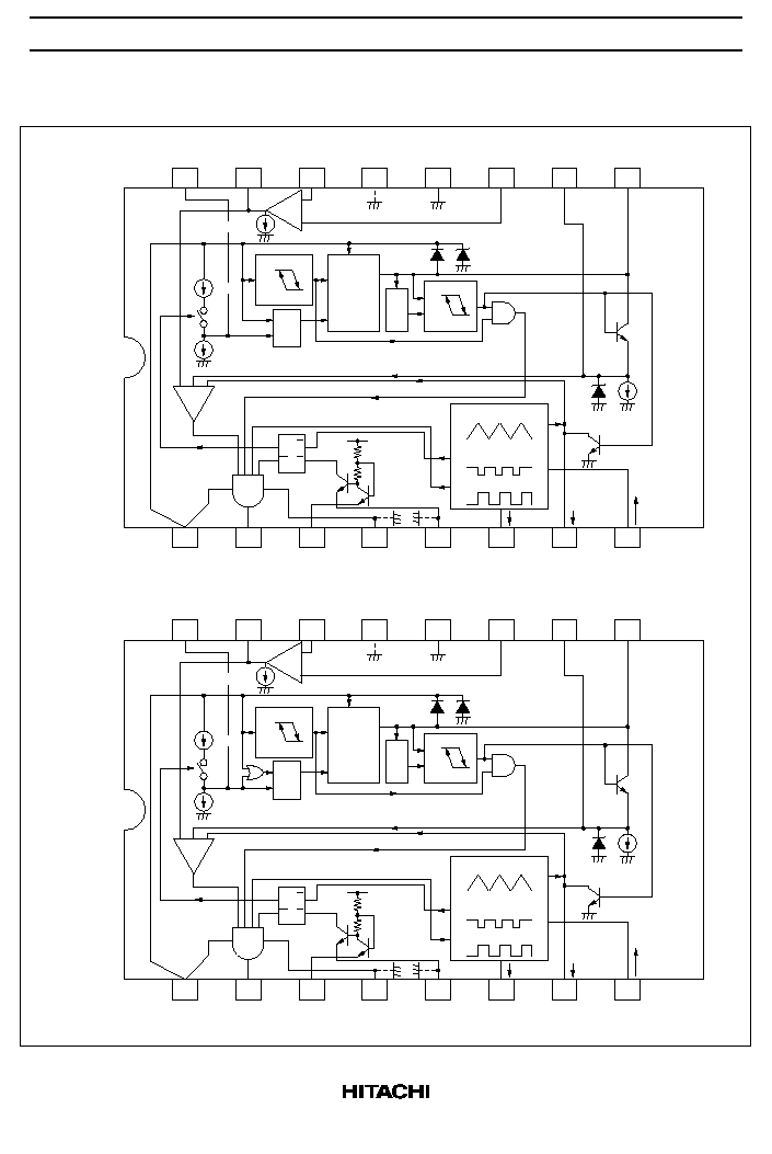
Block Diagram
6.45 V
zener type
Ref.
voltage
Gen.
UVL1
H
L
V
L
V
H
R
S
Q
TL
16
E/O
15
IN (
-
)
14
NC
13
GND
12
IN (+)
11
ST
10
Vref
9
1
V
IN
2
OUT
3
CL (+)
4
V
E
5
CL (
-
)
6
R
T1
7
C
T
8
R
T2
16 A
4 A
On/Off latch
(V
TH
= 7 V)
O
V
P
UVL2
H
L
4 V 5 V
UVL1
ST
Triangle waveform
UVL1 and UVL2
Pulse-by-pulse latch
Q
Q
R
S
OUT
V
E
V
C
QCLM
+ +
-
PWM Comparator
Current
limiter
Triangle waveform OSC
Triangle waveform
Latch reset pulse
ON duty pulse
3.4 V 10 A
34 V
V
IN
UVL2
Vref
Vref
Error amp.
EA
+
-
140 A
6.45 V
zener type
Ref.
voltage
Gen.
UVL1
H
L
V
L
V
H
R
S
Q
ON/OFF
16
E/O
15
IN (
-
)
14
NC
13
GND
12
IN (+)
11
ST
10
Vref
9
1
V
IN
2
OUT
3
CL (+)
4
V
E
5
CL (
-
)
6
R
T1
7
C
T
8
R
T2
16 A
4 A
On/Off latch
(V
TH
= 7 V)
O
V
P
UVL2
H
L
4 V 5 V
UVL1
ST
Triangle waveform
UVL1 and UVL2
Pulse-by-pulse latch
Q
Q
R
S
OUT
V
E
V
C
QCLM
+ +
-
PWM Comparator
Current
limiter
Triangle waveform OSC
Triangle waveform
Latch reset pulse
ON duty pulse
3.4 V 10 A
34 V
V
IN
UVL2
Note: Dotted lines apply to the SOP package model (pins 4, 5, and 13: ground)
Vref
Vref
Error amp.
EA
+
-
140 A
∑
HA16107P/FP
∑
HA16108P/FP