 | –≠–ª–µ–∫—Ç—Ä–æ–Ω–Ω—ã–π –∫–æ–º–ø–æ–Ω–µ–Ω—Ç: HA16116 | –°–∫–∞—á–∞—Ç—å:  PDF PDF  ZIP ZIP |

HA16116FP/FPJ, HA16121FP/FPJ
Switching Regulator for Chopper Type DC/DC Converter
Description
HA16116FP/FPJ and HA16121FP/FPJ are dual-channel PWM switching regulator controller ICs for use in
chopper-type DC/DC converters.
This IC series incorporates totem pole gate drive circuits to allow direct driving of a power MOS FET. The
output logic is preset for booster, step-down, or inverting control in a DC/DC converter. This logic
assumes use of an N-channel power MOS FET for booster control, and a P-channel power MOS FET for
step-down or inverting control.
HA16116 includes a built-in logic circuit for step-down control only, and one for use in both step-down
and inverting control. HA16121 has a logic circuit for booster control only and one for both step-down and
inverting control.
Both ICs have a pulse-by-pulse current limiter, which limits PWM pulse width per pulse as a means of
protecting against overcurrent, and which uses an on/off timer for intermittent operation. Unlike
conventional methods that use a latch timer for shutdown, when the pulse-by-pulse current limiter
continues operation beyond the time set in the timer, the IC is made to operate intermittently (flickering
operation), resulting in sharp vertical setting characteristics. When the overcurrent condition subsides, the
output is automatically restored to normal.
The dual control circuits in the IC output identical triangle waveforms, for completely synchronous
configuring a compact, high efficiency dual-channel DC/DC converter, with fewer external components
than were necessary previously.
Functions
∑
2.5 V reference voltage (Vref) regulator
∑
Triangle wave form oscillator
∑
Dual overcurrent detector
∑
Dual totem pole output driver
∑
UVL (under voltage lock out) system
∑
Dual error amplifier
∑
Vref overvoltage detector
∑
Dual PWM comparator

HA16116FP/FPJ, HA16121FP/FPJ
2
Features
∑
Wide operating supply voltage range* (3.9 V to 40.0 V)
∑
Wide operating frequency range (600 kHz maximum operation)
∑
Direct power MOS FET driving (output current ±1 A peak in maximum rating)
∑
Pulse-by-pulse overcurrent protection circuit with intermittent operation function (When overcurrent
state continues beyond time set in timer, the IC operates intermittently to prevent excessive output
current.)
∑
Grounding the ON/
OFF pin turns the IC off, saving power dissipation. (HA16116: I
OFF
= 10
µ
A max.;
HA16121: I
OFF
= 150
µ
A max.)
∑
Built-in UVL circuit (UVL voltage can be varied with external resistance.)
∑
Built-in soft start and quick shutoff functions
Note:
The reference voltage 2.5 V is under the condition of V
IN
4.5 V.
Ordering Information
Hitachi Control ICs for Chopper-Type DC/DC Converters
Product
Channel
Control Functions
Overcurrent
Channels
Number
No.
Step-Up
Step-Down
Inverting
Output Circuits
Protection
Dual
HA17451
Ch 1
r
r
r
Open collector
SCP with timer (latch)
Ch 2
r
r
r
Single
HA16114
--
--
r
r
Totem pole
Pulse-by-pulse
HA16120
--
r
--
--
power MOS FET
current limiter and
Dual
HA16116
Ch 1
--
r
r
driver
intermittent operation
Ch 2
--
r
--
by on/off timer
HA16121
Ch 1
--
r
r
Ch 2
r
--
--

HA16116FP/FPJ, HA16121FP/FPJ
3
Pin Arrangement
1
2
3
4
5
6
7
8
9
10
20
19
18
17
16
15
14
13
12
11
S.GND
CT
RT
IN(+)1
IN(
-
)1
E/O1
DB1
CL1
OUT1
P.GND
S.V
Vref
TIM
ON/OFF
IN(
-
)2
E/O2
DB2
CL2
OUT2
P.V
IN
IN
*
*
2
2
*
*
1
1
(top view)
Notes:
Channel 2
Channel 1
1.
2.
Pins S.GND (pin 1) and P.GND (pin 10) have no direct internal interconnection.
Both pins must be connected to ground.
Pins S.V (pin 20) and P.V (pin 11) have no direct internal interconnection.
Both pins must be connected to V .
IN
IN
IN

HA16116FP/FPJ, HA16121FP/FPJ
4
Pin Functions
Pin No.
Symbol
Function
1
S.GND
Signal circuitry*
1
ground
2
C
T
Timing capacitance (triangle wave oscillator output)
3
R
T
Timing resistance (for bias current synchronization)
4
IN(+)1
Error amp. noninverting input (1)
Channel 1
5
IN(≠)1
Error amp. inverting input (1)
6
E/O1
Error amp. output (1)
7
DB1
Dead band timer off period adjustment input (1)
8
CL1
Overcurrent detection input (1)
9
OUT1
PWM pulse output (1)
10
P.GND
Output stage*
1
ground
11
P.V
IN
Output stage*
1
power supply input
12
OUT2
PWM pulse output (2)
Channel 2
13
CL2
Overcurrent detection input (2)
14
DB2
Dead band timer off period adjustment input (2)
15
E/O2
Error amp. output (2)
16
IN(≠)2
Error amp. inverting input (2)*
2
17
ON/
OFF
IC on/off switch input (off when grounded)
18
TIM
Setting of intermittent operation timing when overcurrent is detected
(collector input of timer transistor)
19
Vref
2.5 V reference voltage output
20
S.V
IN
Signal circuitry*
1
power supply input
Notes: 1. Here "output stage" refers to the power MOS FET driver circuits, and "signal circuitry" refers to all
other circuits on the IC. Note that this IC is not protected against reverse insertion, which can
cause breakdown of the IC between V
IN
and GND. Be careful to insert the IC correctly.
2. Noninverting input of the channel 2 error amp is connected internally to Vref.
HA16116FP/FPJ, HA16121FP/FPJ
5
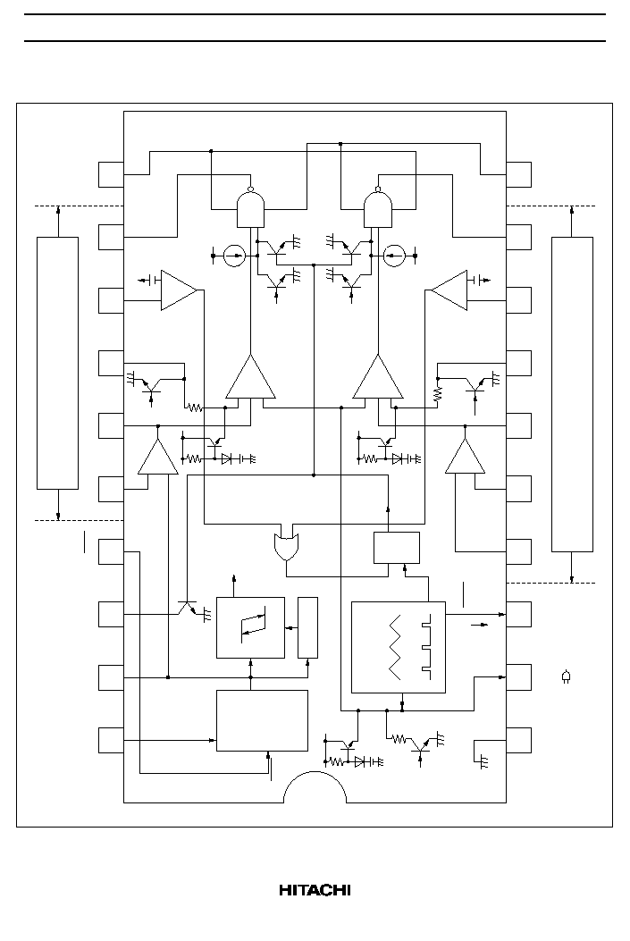
Block Diagram
S.V
20
V
ref
19
TIM
18
ON/OFF
17
IN(
-
)2
16
E/O2
15
DB2
14
CL2
13
OUT2
12
P
.V
11
IN
IN
1
S.GND
2
C
3
R
4
IN(+)1
5
IN(
-
)1
6
E/O1
7
DB1
8
CL1
9
OUT1
10
P
.GND
TT
from
UVL
1.1 V
R
T
S
R
Q
OR
OVP
UVL
H
L
V
L
V
H
+
-
EA1
from
UVL
-
+
+
+
+
-
PWM COMP
2
from
UVL
PWM COMP
1
5k
5k
5k
from UVL
from UVL
V
ref
V
ref
OUT2
OUT1
*
NAND
(HA161
16)
NAND
0.2 V
-
+
CL2
CL1
to S.V
IN
to S.V
IN
-
+
0.2 V
1.6 V
1.0 V
-
+
EA2
UVL
output
Latch
V
IN
0.8V
V
IN
0.8V
V
IN
0.8V
[Channel 2]
Step-down control only (HA161
16)
Booster control only (HA16121)
[Channel 1] (HA161
16/HA16121)
Step-down or inverting control
ON/OFF
T
riangle wave
oscillator circuit
triangle wave
latch reset pulse
Bias current
2.5 V output
band gap
reference
voltage
generator
circuit
Note:
This block is
AND ( ) in the case of
HA16121.
*