 | –≠–ª–µ–∫—Ç—Ä–æ–Ω–Ω—ã–π –∫–æ–º–ø–æ–Ω–µ–Ω—Ç: HA16141P | –°–∫–∞—á–∞—Ç—å:  PDF PDF  ZIP ZIP |
HA16141P/FP, HA16142P/FP
PFC and PWM Controller
ADE-204-036D (Z)
Preliminary
Rev. 4
Sep. 2001
Description
The HA16141P/FP and the HA16142P/FP are power supply controller ICs combining an AC-DC converter
switching controllers for power factor correction and off-line power supply switching controllers. PFC
(Power factor correction) section employs average current mode PWM and off-line power supply control
section employs peak current mode PWM.
The HA16142P/FP is the change version of HA16141P/FP's PWM maximum on duty cycle.
The PFC operation can be turned on and off by external control signal. Use of this on/off function makes it
possible to disable PFC operation at a low line voltage, or to perform remote control operation from the
transformer secondary side. The PFC power supply boosted output voltage is not only fed to an error
amplifier input signal but also fed to as the boost voltage monitor circuit.
PG signal is put out if the boost
voltage is out-of-spec.
The PWM controller, which begins operation at the same time as release of the IC's UVLO (under-voltage
lockout) is suitable for auxiliary power supply use in a multi-output power supply system.
Features
∑ Synchronized PFC and PWM timing
∑ Self oscillation with fixed frequency
PFC
: 100 kHz (
±15 %)
PWM : 200 kHz (
±15 %)
∑ PFC function on/off control
∑ PFC boosted output voltage monitor
∑ High-output current gate drivers
PFC driver peak current
:
±1.5 A typ.
PWM driver peak current :
±1.0 A typ.
∑ PWM maximum on duty cycle
72% min (HA16141P/FP)
49.5% max (HA16142P/FP)

HA16141P/FP, HA16142P/FP
Rev.4, Sep. 2001, page 2 of 18
Pin Arrangement
(Top view)
1
2
3
4
5
6
7
8
PWM-CS
PWM-EO
O.C
PFC-EO
TIM
PFC-FB
IAC
PFC-ON
16
15
14
13
12
11
10
9
GND
PWM-OUT
PFC-OUT
VCC
VREF
PG
CAO
PFC-CS
Pin Description
Pin No.
Symbol
Function
1
GND
Ground
2
PWM-OUT
Power MOS FET driver output (PWM control)
3
PFC-OUT
Power MOS FET driver output (PFC control)
4
VCC
Supply voltage
5
VREF
Reference voltage
6
PG
Power Good signal output (open-drain output)
7
CAO
Average current control error amp. output
8
PFC-CS
PFC control current sense signal input
9
PFC-ON
PFC function on/off signal input
10
IAC
Multiplier reference current input
11
PFC-FB
PFC control error amp. input
12
TIM
Overcurrent timer time setting
13
PFC-EO
PFC control error amp. output
14
O.C
Overcurrent detector signal input
PWM control error amp. output (photocoupler input also possible) (HA16141 only)
15
PWM-EO
PWM control feedback voltage signal input (HA16142 only)
16
PWM-CS
PWM control current sense signal input
HA16141P/FP, HA16142P/FP
Rev.4, Sep. 2001, page 3 of 18
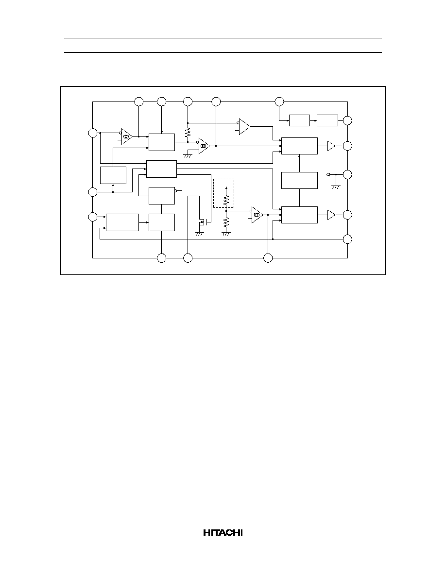
Block Diagram
13
11
2.5V
-0.5V
PFC-FB
14
O.C
9
PFC-ON
PFC-EO
PFC-V
AMP
PWM-V
AMP
PFC-C
AMP
PFC-C
LIMIT
7
CAO
4
5 VREF
1 GND
2 PWM-OUT
16 PWM-CS
3 PFC-OUT
VCC
10
IAC
2.5V
100kHz
±1.5A
200kHz
Multiplier
Integrator
LATCH
RES
VCC
VCC
5R
2.7k
PFC/PWM
Supervisor
±1.0A
Over
Current Det.
Gain
Selector
8
PFC-CS
PFC Control
UVLO
VREF
Oscillator
PWM Control
R
12
6
TIM
15
PWM-EO
2/
HA16141 only

HA16141P/FP, HA16142P/FP
Rev.4, Sep. 2001, page 4 of 18
System Diagram
CAO
VCC
CT
3.3n
36k
VREF
Rec+
1.8m
Q1
B+
B+ OUT
GND
(385V dc)
T1
+
Rec
-
PWM-RES
PFC-DT
+B HIGH
RAMP
22.2V
100
220p
I
AC
I
MO
IAC
I
MO
= K {I
AC
◊ (V
EO
- 1V)}
PFC-C
AMP
PFC-V
AMP
PWM-V
AMP
◊1
Gain Selector
Over
Current
Detector
Integrator
Latch Block
910k
K
V
EO
2.7k
0.1
(5W)
TIM
PG
PFC
-CS
PFC
-EO
47n
750k
PFC
-FB
PFC
-ON
GND
Note: The constants for the external components are for reference. Please confirm the operation when designing the system.
4.7n
From
VRB(B+monitor)
55k
-0.5V
VREF
PFC-C
LIMIT
-
+
-
+
+
-
+
-
+
+B LOW
PFC-OFF
PWM-OFF
Circuit Ground Level
2.5V
2.75V
2.60V
2.5V
RB
3.83V
3.63V
R
Q
Supervisor
K = 0.25
S
R
PWM-RES
Q
S
R
Q
S
H
UVLO
L
H
VREF
GOOD
VREF
GOOD
VREF
GOOD
Gate Driver
±1.5A(PEAK)
Gate Driver
±1A(PEAK)
UVL
L
5V VREF
Generator
5V Internal Bias
-
+
-
+
-
K = 0.05
LOGIC
2.34V
1.70V
+
-
1.5V
1.2V
0.1
µ
51k
5.1k
VREF
Enable to
secondary
33k
720k
2.2
µ
+
-
1V
0.3V
5V
4V
VCC
LOGIC
2.5V
+
-
+
-
PWM
-CS
2R
R
5RB
VCC
0.1
(1W)
1
(1W)
To T1
To
Q1 gate
From PFC-OUT
From
Q2 drain
To
PFC-FB
Current Monitor
Unit R:
C: F
+
-
+
-
7.1V
0.1
µ
38.2
µ
3V
26.2
µ
5.2
µ
Q
S
R
Q
R
S
+
-
-
+
O.C
VREF
PWM
-EO
PWM
-OUT
PFC
-OUT
1n
0.1
µ
0.47
µ
470
µ
(600V)
1n
51k
+
4.7
µ
570k
(1/2W)
710k
VRB
4.7k
100kHz
3.4V
0.65V
200kHz
Oscillator
500ns
10
µs
5
µs
1
µs (HA16141)
2.3
µs (HA16142)
820k
10n
HA16141 only
External parts of
PWM-EO pin are
applies to HA16141
only.
HA16141P/FP, HA16142P/FP
Rev.4, Sep. 2001, page 5 of 18
Absolute Maximum Ratings
(Ta = 25
∞C)
Item
Symbol
Rating
Unit
Note
Supply voltage
V
CC
20
V
Peak PFC-OUT current
Ipk-pfc
±1.5
A
3
Peak PWM-OUT current
Ipk-pwm
±1.0
A
3
DC PFC-OUT current
Idc-pfc
±0.15
A
DC PWM-OUT current
Idc-pwm
±0.10
A
Vi-group1
-0.3 to V
CC
V
4
Terminal voltage
Vi-group2
-0.3 to Vref
V
5
CAO voltage
Vcao
-0.3 to Veoh-ca
V
PFC-EO voltage
Vpfc-eo
-0.3 to Veoh-pfc
V
PWM-EO voltage
Vpwm-eo
-0.3 to Veoh-pwm
V
PFC-ON voltage
Vpfc-on
-0.3 to +7
V
IAC voltage
Vi-ac
-0.3 to +5
V
IAC current
Ii-ac
0.8
mA
PFC-CS voltage
Vi-cs
-1.5 to +0.3
V
TIM voltage
Vi-tim
-0.3 to +6
V
VREF current
Io-ref
-20
mA
PG voltage
Vo-pg
-0.3 to +7
V
PG current
Io-pg
15
mA
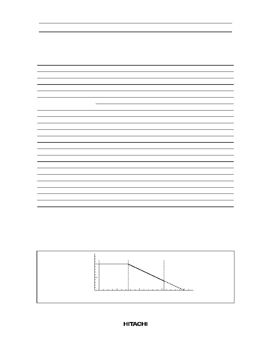
Power dissipation
P
T
1
W
6
Operating temperature
Topr
-40 to +105
∞C
Storage temperature
Tstg
-55 to +150
∞C
Junction temperature
Tj
150
∞C
Notes: 1. Rated voltages are with reference to the GND pin.
2. For rated currents, inflow to the IC is indicated by (+), and outflow by (
-).
3. Shows the transient current when driving a capacitive load.
4. Group1 is the rated voltage for the following pins: PFC-OUT, PWM-OUT
5. Group2 is the rated voltage for the following pins: VREF, PFC-FB, PWM-CS
6. This is the value when the ambient temperature (Ta) is 25
∞C or below. If Ta exceeds 25∞C, the
graph below applies. For the SOP package, this value is based on actual measurements on a
10% wiring density glass epoxy circuit board (40 mm
◊ 40 mm ◊ 1.6 mm).
1
0.5
0
-40
0
50
100
150
25
∞C
-8mW/∞C
105
∞C
Ambient temperature Ta (
∞C)
Maximum power
dissipation P
T
(W)

HA16141P/FP, HA16142P/FP
Rev.4, Sep. 2001, page 6 of 18
Electrical Characteristics
(Ta = 25
∞C, V
CC
= 14 V)
Item
Symbol
Min
Typ
Max
Unit
Test Conditions
Start threshold
V
H
12.2
13.0
13.8
V
Shutdown threshold
V
L
9.4
10.0
10.6
V
UVLO hysteresis
dV
UVL
2.6
3.0
3.4
V
Start-up current
I
S
150
200
300
µA
V
CC
= 12V
Is temperature stability
dI
S
/dTa
-0.3
%/
∞C
*
1
Operating current
I
CC
4
7
9
mA
IAC = 100
µA, C
L
= 0F
Latch current
I
LATCH
230
310
375
µA
V
CC
= 9V
Shunt zener voltage
V
Z
21.2
22.2
23.2
V
I
CC
= 14mA
Supply
Vz temperature stability
dV
Z
/dTa
+4
mV/
∞C
I
CC
= 14mA *
1
Minimum duty cycle
Dmin-pfc
0
%
CAO = 3.6V
Maximum duty cycle
Dmax-pfc
90
95
98
%
CAO = 0V
Rise time
t
r
-pfc
30
100
ns
C
L
= 1000p
Fall time
t
f
-pfc
30
100
ns
C
L
= 1000p
Peak current
Ipk-pfc
1.5
A
C
L
= 0.01
µF *
1
Vol1-pfc
0.05
0.2
V
Iout = 20mA
Vol2-pfc
0.35
1.4
V
Iout = 200mA
Low voltage
Vol3-pfc
0.03
0.7
V
Iout = 10mA, V
CC
= 5V
Voh1-pfc
13.5
13.9
V
Iout =
-20mA
PFC-OUT
High voltage
Voh2-pfc
12.6
13.3
V
Iout =
-200mA
Minimum duty cycle
Dmin-pwm
0
%
PWM-EO = 1.3V
PWM-CS = 0V
72
80
88
%
PWM-EO = 5V
PWM-CS = 0V *
2
Maximum duty cycle
Dmax-pwm
42.5
46
49.5
%
PWM-EO = 5V
PWM-CS = 0V *
3
Rise time
t
r
-pwm
30
100
ns
C
L
= 1000p
Fall time
t
f
-pwm
30
100
ns
C
L
= 1000p
Peak current
Ipk-pwm
1.0
A
C
L
= 0.01
µF *
1
Vol1-pwm
0.05
0.2
V
Iout = 20mA
Vol2-pwm
0.5
2.0
V
Iout = 200mA
Low voltage
Vol3-pwm
0.03
0.7
V
Iout = 10mA, V
CC
= 5V
Voh1-pwm
13.5
13.9
V
Iout =
-20mA
PWM-OUT
High voltage
Voh2-pwm
12.0
13.0
V
Iout =
-200mA
Output voltage
Vref
4.9
5.0
5.1
V
Isource = 1mA
Line regulation
Vref-line
5
20
mV
Isource = 1mA
V
CC
= 12V to 18V
Load regulation
Vref-load
5
20
mV
Isource = 1mA to 20mA
VREF
Temperature stability
dVref
80
ppm/
∞C
Ta =
-40 to 105∞C *
1
Note:
1. Design spec.
2. Apply to HA16141.
3. Apply to HA16142.
HA16141P/FP, HA16142P/FP
Rev.4, Sep. 2001, page 7 of 18
Electrical Characteristics
(Ta = 25
∞C, V
CC
= 14 V) (cont.)
Item
Symbol
Min
Typ
Max
Unit
Test Conditions
fpwm
170
200
230
kHz
Measured pin: PWM-OUT
Initial accuracy
fpfc
85
100
115
kHz
Measured pin: PFC-OUT
fpwm temperature
stability
dfpwm/dTa
±0.1
%/
∞C
Ta =
-40 to 105∞C *
1
fpwm voltage stability
fpwm(line)
-1.5
+0.5
+1.5
%
V
CC
= 12V to 18V
Ramp peak voltage
Vramp-H
3.4
3.6
V
Oscillator
Ramp valley volatge
Vramp-L
0.65
V
*
1
PFC on voltage
Von-pfc
1.3
1.5
1.7
V
PFC off voltage
Voff-pfc
1.0
1.2
1.4
V
PFC on-off hysteresis
dVon-off
0.15
0.30
0.45
V
PFC-ON
Input current
Ipfc-on
0.1
1.0
µA
PFC-ON = 2V
PFC GOOD
threshold voltage
Vb-good
2.29
2.34
2.39
V
Input pin: PFC-FB
PFC FAIL
threshold voltage
Vb-fail
1.66
1.70
1.74
V
Input pin: PFC-FB
+B High
PFC inhibit voltage
Vb-h
2.69
2.75
2.81
V
Input pin: PFC-FB
+B High
PFC restart voltage
Vb-res
2.54
2.60
2.66
V
Input pin: PFC-FB
PG leak current
Ioff-pg
0.001
1.0
µA
PG = 5V
PG shunt current
Ion-pg
5
15
mA
PG = 3V *
2
Supervisor/
PG
Delay to
PG
tg-pg
0.2
1
µs
Step signal (5 to 0V) to
PFC-ON
O.C threshold voltage
V
OC
0.27
0.30
0.33
V
PWM-CS threshold
voltage
V
CS
0.9
1.0
1.1
V
O.C
(Over Current
Detector)
O.C input current
I
OC
-0.1
-1.0
µA
O.C = 0V
Sink current
Isnk-tim
3.9
5.2
6.5
µA
TIM = 2V
Source current
O.C trigger
Isrc-tim1
-16
-21
-26
µA
TIM = 2V, O.C = 0.5V *
1
Source Current
PWM-CS trigger
Isrc-tim2
-25
-33
-41
µA
TIM = 2V, PWM-CS = 2V *
1
Integrated time
O.C trigger
t-tim1
88
110
132
µs
Step signal (0 to 1V) to
O.C, Ctim = 1000p,
Measured pin:
PG
Integrator
Integrated Time
PWM-CS trigger
t-tim2
53
67
81
µs
Step signal (0 to 2V) to
PWM-CS, Ctim = 1000p,
Measured pin:
PG
Notes: 1. Design spec.
2. Maximum rating of PG current is 15 mA. Use series resistor to limit PG current lower than 15
mA.

HA16141P/FP, HA16142P/FP
Rev.4, Sep. 2001, page 8 of 18
Electrical Characteristics
(Ta = 25
∞C, V
CC
= 14 V) (cont.)
Item
Symbol
Min
Typ
Max
Unit
Test Conditions
Threshold voltage
for PFC stop
Vlch-pfc
2.4
2.5
2.6
V
Input pin: TIM
Threshold Voltage
for PWM stop
Vlch-sys
3.8
4.0
4.2
V
Input pin: TIM
Latch
Latch Reset Voltage
Vcc-res
6.1
7.1
8.1
V
Feedback V
CC
voltage
Vfb-pwm
14.2
14.8
15.4
V
PWM-EO = 2.5V *
2
Open loop gain
Av-pwm
45
dB
*
1,
*
2
High voltage
Veoh-pwm
5.1
5.7
6.3
V
V
CC
= 14V,
PWM-EO: Open
Low voltage
Veol-pwm
0.1
0.3
V
V
CC
= 16V,
PWM-EO: Open *
2
Source current
Isrc-pwm
-77
µA
*
1
V
CC
= 11V
Sink current
Isnk-pwm
77
µA
*
1
V
CC
= 18V *
2
PWM-V
AMP
Transconductance
respect to V
CC
Gm-pwm
19
27
35
µA/V
V
CC
= 15V,
PWM-EO = 2.5V *
2
PWM current
sense
Delay to output
td-cs
210
300
ns
PWM-EO = 5V,
PWM-CS = 0 to 2V
Threshold voltage
V
LM
-0.47
-0.50
-0.53
V
PFC current
limit
Delay to output
td-
LM
280
500
ns
PFC-CS = 0 to
-1V
Feedback voltage
Vfb-pfc
2.45
2.50
2.55
V
PFC-EO = 2.5V
Input bias current
Ifb-pfc
-0.30
-0.07
+0.30
µA
Measured pin: PFC-FB
Open loop gain
Av-pfc
65
dB
*
1
High voltage
Veoh-pfc
5.1
5.7
6.3
V
PFC-FB = 2.3V,
PFC-EO: Open
Low voltage
Veol-pfc
0.1
0.3
V
PFC-FB = 2.7V,
PFC-EO: Open
Source current
Isrc-pfc
-62
-77
-93
µA
PFC-FB = 1.0V,
PFC-EO = 2.5V
Sink current
Isnk-pfc
62
77
93
µA
PFC-FB = 4.0V,
PFC-EO = 2.5V
PFC-V
AMP
Transconductance
Gm-pfcv
120
160
200
µA/V
PFC-FB = 2.5V,
PFC-EO = 2.5V
Note:
1. Design spec.
2. Apply to HA16141.

HA16141P/FP, HA16142P/FP
Rev.4, Sep. 2001, page 9 of 18
Electrical Characteristics
(Ta = 25
∞C, V
CC
= 14 V) (cont.)
Item
Symbol
Min
Typ
Max
Unit
Test Conditions
Input offset voltage
Vio-ca
±7
mV
*
1
Open loop gain
Av-ca
65
dB
*
1
High voltage
Veoh-ca
5.1
5.7
6.3
V
Low voltage
Veol-ca
0.1
0.3
V
Source current
Isrc-ca
-77
µA
CAO = 2.5V *
1
Sink current
Isnk-ca
77
µA
CAO = 2.5V *
1
PFC-C
AMP
Transconductance
Gm-pfcc
120
160
200
µA/V
*
1
IAC PIN voltage
Viac
0.7
1.0
1.3
V
IAC = 100
µA
Terminal offset current
Imo-offset
-56
-75
-94
µA
IAC = 0A, PFC-CS = 0V,
Measured pin: PFC-CS
Imo1
-25
µA
PFC-EO = 2V,
IAC = 100
µA *
1,
*
2
Output current
(PFC-ON = 3.4V)
Imo2
-75
µA
PFC-EO = 4V,
IAC = 100
µA *
1,
*
2
Imo3
-5
µA
PFC-EO = 2V,
IAC = 100
µA *
1,
*
2
Output current
(PFC-ON = 3.9V)
Imo4
-15
µA
PFC-EO = 4V,
IAC = 100
µA *
1,
*
2
IAC/
Multiplier
PFC-CS resistance
Rmo
2.7
k
*
1
Threshold voltage
for K = 0.05
V
K-H
3.71
3.83
3.95
V
Threshold voltage
for K = 0.25
V
K-L
3.51
3.63
3.75
V
Gain
selector
V
K
hysteresis voltage
dV
K
0.15
0.20
0.25
V
*
1
Notes: 1. Design spec.
2. Imo
1
to Imo
4
are defined as,
Imo = (PFC-CS Terminal Current)
- (Imo-offset)
I
AC
Imo
IAC
Imo = K {I
AC
◊ (V
EO
- 1V)}
PFC-C
AMP
PFC-CS Terminal
Current
Imo-offset
K
V
EO
2.7k
PFC-CS
55k
-0.5V
VREF
PFC-C
LIMIT
-
+
-
+
-
+

HA16141P/FP, HA16142P/FP
Rev.4, Sep. 2001, page 10 of 18
Internal Timing
1. UVLO
VCC
VREF
VREF GOOD
(internal signal)
5V
0V
0V
13V
10V
4.6V
System Enable
2. Oscillator, Gate driver output
Reference
triangle wave CT
200 kHz
(internal signal)
Note: All numeric values in the figure are typical values.
PWM-RES
(internal signal)
PFC-DT
(internal signal)
PFC triangle wave
Ramp
100 kHz
(internal signal)
PFC current amp.
output
CAO
PWM current sense
PWM-CS
PWM-OUT
(Trailing Edge control)
PFC-OUT
(Leading Edge control)
3.2V
1.6V
3.4V
0.65V
PWM voltage feedback
(internal signal)

HA16141P/FP, HA16142P/FP
Rev.4, Sep. 2001, page 11 of 18
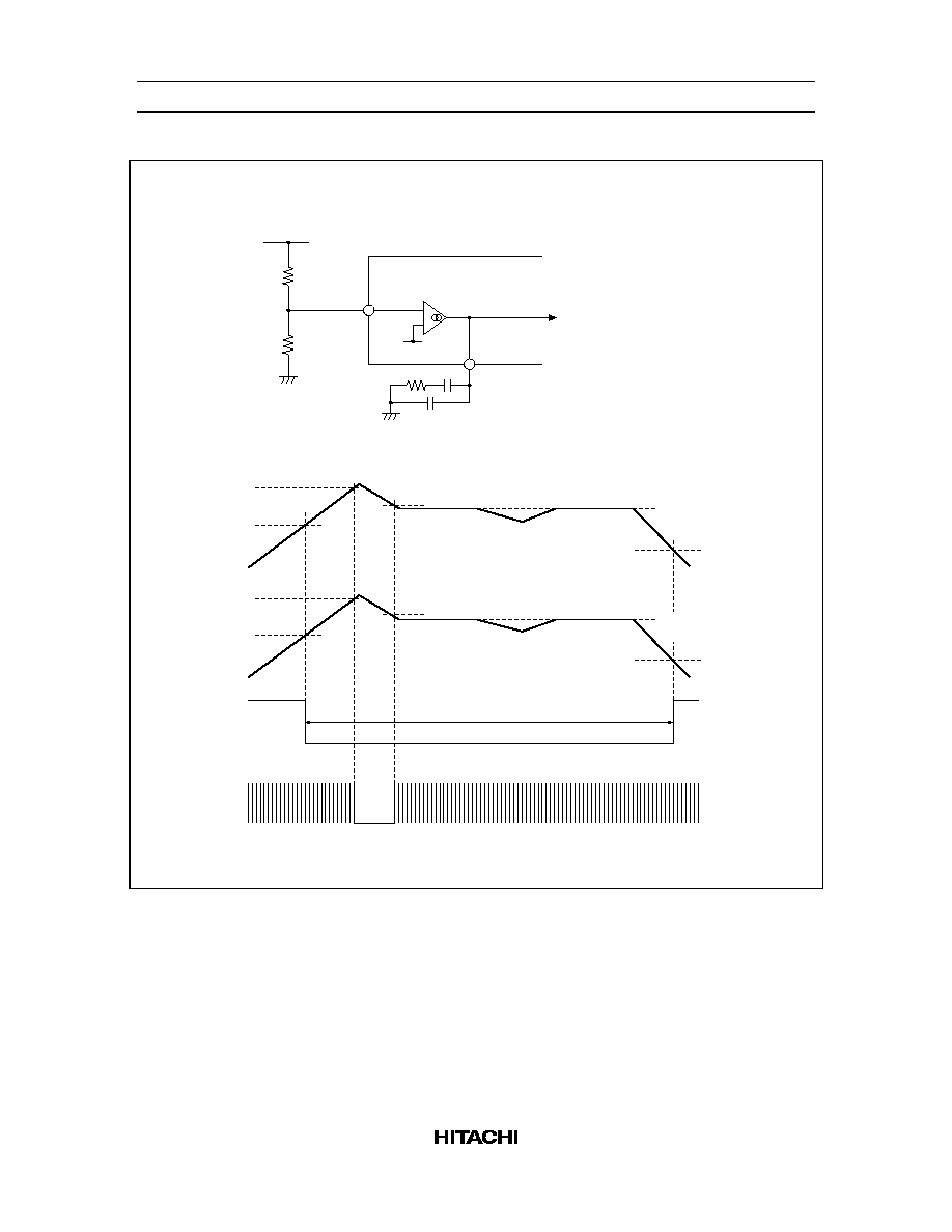
3. PFC controller status
PFC-ON
PFC-FB
1.2V
Notes: 1.
2.
3.
All numeric values in the figure are typical values.
PFC-ON
The HA16141P/FP can perform on/off control of the PFC function using the PFC-ON pin.
If an AC voltage that has undergone primary rectification and has been divided with an external resistance is input,
PFC stoppage is possible in the event of a low input voltage.
On/off control by means of a logic signal is also possible.
PFC-FB
The input to this pin is the voltage obtained by dividing the stepped-up PFC output voltage.
The pin voltage is fed back to the PFC control system, and is also used for step-up voltage logic decisions.
This is outlined in the figure below.
2.34V
Precondition: VREF GOOD, Non latched.
1.5V
PG
PFC-OUT
2.75V
2.60V
1.5V
1.70V
2.34V
1.2V
PG signal high due to
low PFC-FB voltage
Normal
operation
PFC pulses stopped due to
high PFC-FB voltage
(overshoot prevention)
PFC pulses stopped
by PFC-ON,
and PG signal high
2.34V
2.75V
2.60V
1.70V
Hysteresis
Hysteresis
PFC-OUT pulse stoppage
(Reduction of step-up voltage overshoot)
PG
(Power Good) signal is output
Feedback voltage
2.50V
(Note 3 is continued on the next page)
PFC pulses stopped
by PFC-ON,
and PG signal high
PFC pulses stopped
by PFC-ON,
and PG signal high
PG signal high due to
low PFC-FB voltage
Normal
operation
Normal
operation
Normal
operation
HA16141P/FP, HA16142P/FP
Rev.4, Sep. 2001, page 12 of 18
3. PFC controller status (cont.)
Step-up voltage
+B
356V
418V
395V
259V
380V
(Typical Output Voltage)
PFC-FB
2.34V
2.75V
2.60V
1.70V
PFC-OUT
PG
2.5V
(PFC Feedback Voltage)
Precondition: VREF GOOD, PFC-ON, Non latched.
Power Good Period
To Multiplier
Notes:
+B
R1
3.
Notes: 4.
PFC-FB (cont.)
The actual input voltage to the PFC-FB pin is the step-up voltage divided with a resistance (see figure below).
If R1 is set as 710 kW and R2 as 4.7 kW, the decision voltage at the step-up pin (+B) is as shown in the figure below.
All numeric values in the figure are typical values.
-
+
R2
710kW
2.5V
PFC-V
AMP
PFC-FB
PFC-EO
4.7kW
HA16141P/FP, HA16142P/FP
Rev.4, Sep. 2001, page 13 of 18
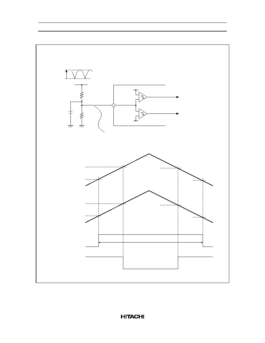
4. PFC-ON pin
AC voltage
Vac
Note: All numeric values in the figure are typical values.
157Vac
PFC Status
(internal status)
Precondition: VREF GOOD, Non latched.
PFC-ON Period
Em
0Vac
62Vac
149Vac
49Vac
PFC-ON
3.83V
0V
1.5V
3.63V
1.2V
OFF
ON
Multiplier gain
(internal status)
0.05
0.25
The following functions are effected by inputting an AC voltage that has undergone primary rectification
and has been divided with an external resistance to the PFC-ON pin (see figure below).
a) Turning PFC operation off when AC voltage is low
b) Switching multiplier gain with AC 100 V system and 200 V system input
Rec+
R1
Switching Multiplier Gain
-
+
R2
2.2mF
720kW
3.83V
3.63V
1.5V
1.2V
PFC-ON
20kW
PFC-ON/OFF Control
-
+
PFC-ON(dc) = 2 ◊ Em / p ◊ R2 / (R1 + R2)
= 2 ◊ (÷2) ◊ Vac / p ◊ R2 / (R1 + R2)

HA16141P/FP, HA16142P/FP
Rev.4, Sep. 2001, page 14 of 18
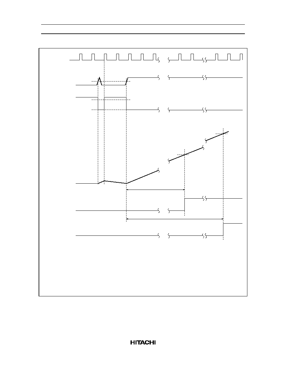
5. Integrator (OC detection operation)
PWM-RES
(internal signal)
O.C
(overcurrent
detection input)
TIM pin current
(integral output
current)
TIM pin voltage
(integral output
voltage)
LATCH STATUS
(for PFC-STOP)
LATCH STATUS
(for PWM-STOP)
0.3V
0
5.2
µA
-21µA
2.5V
0.2V
PFC Enable
PWM Enable
PFC Stop
3V
t-tim1
Note: Timer time calculation equation
Timer time t-tim1 is the time until PG pin inversion (from low to high) after the O.C pin trigger.
t-tim1 can be set using the following approximate equation.
t-tim1 =
-Ctim (Vlch - pfc - 0.2V) / Isrc - tim1
=
-Ctim (2.5V - 0.2V) / (-21µA) Typical calculation
HA16141P/FP, HA16142P/FP
Rev.4, Sep. 2001, page 15 of 18
6. Integrator (PWM-CS detection operation)
PWM-RES
(internal signal)
PWM-CS
(current sense
input)
TIM pin current
(integral output
current)
TIM pin voltage
(integral output
voltage)
LATCH STATUS
(for PFC-STOP)
LATCH STATUS
(for PWM-STOP)
1V
0
5.2
µA
-33µA
2.5V
4V
0.2V
PFC Enable
PWM Enable
PFC Stop
PWM Stop
t-tim2
t-tim2'
Note: Timer time calculation equation
Timer time t-tim2 is the time until PG pin inversion (from low to high) after the PWM-CS pin trigger.
t-tim2 can be set using the following approximate equation.
t-tim2
The time at which both the PFC and PWM functions are stopped by this timer can be calculated
using the following approximate equation.
t-tim2' = 1.65
t - tim2 Typical calculation
=
-Ctim (Vlch - pfc - 0.2V) / Isrc - tim2
=
-Ctim (2.5V - 0.2V) / (-33µA) Typical calculation
HA16141P/FP, HA16142P/FP
Rev.4, Sep. 2001, page 16 of 18
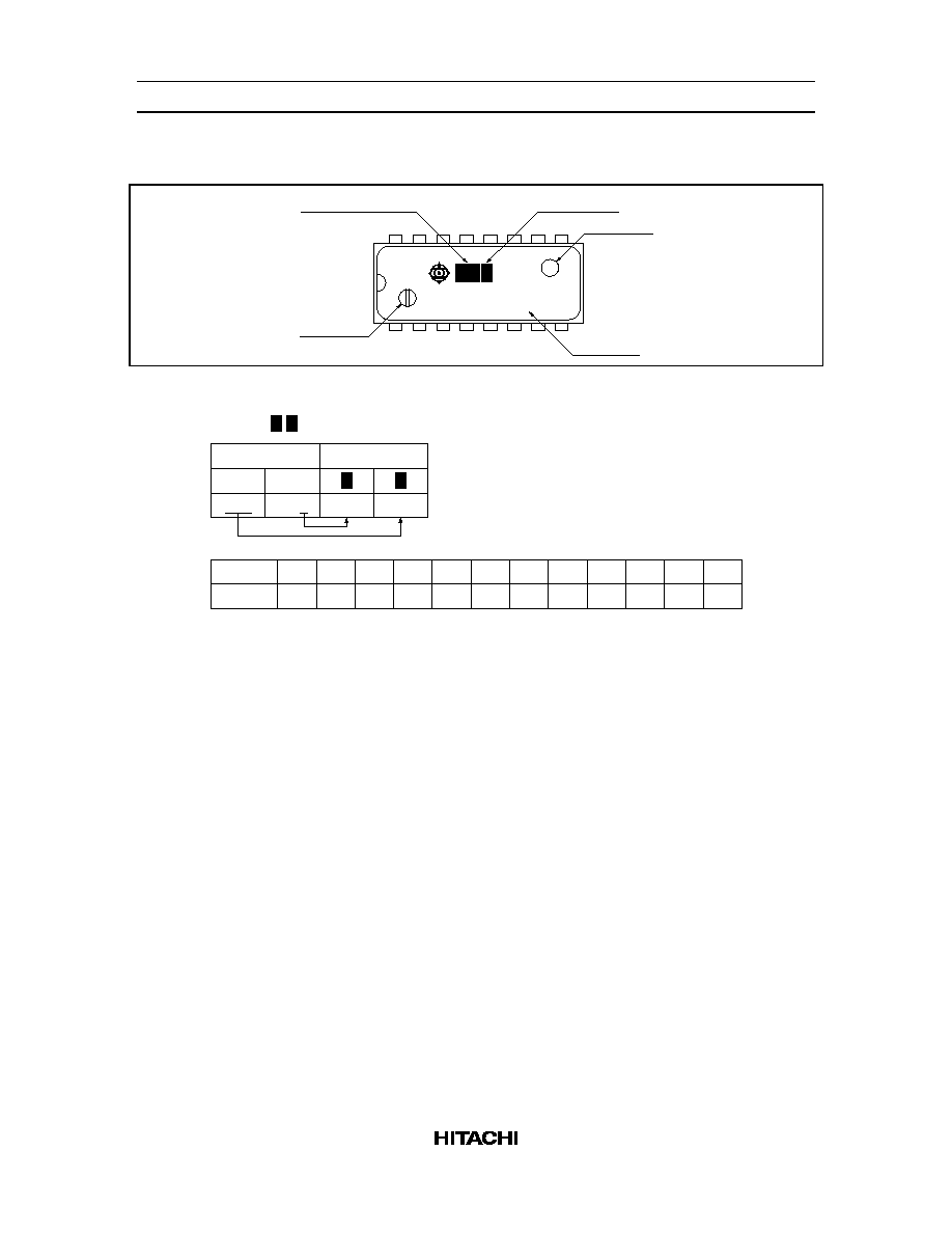
Mark Pattern
Ejector pin
Ejector pin
Type code
Control code
1, 2: Lot indication
HA16141P
(HA16142P)
1 2 3
Notes: 1. Example of lot indication.
For example, a product manufactured in May 2000 has the markings "0E" in
positions in the above figure.
Production
Month
May
Month
Code
Jan
A
Mar
C
Feb
B
Apr
D
Jun
F
May
E
Jul
G
Sep
J
Aug
H
Oct
K
Dec
M
Nov
L
Year
2000
Indication
0
E
1
1
2
2
2. Laser marking is used.
HA16141P/FP, HA16142P/FP
Rev.4, Sep. 2001, page 17 of 18
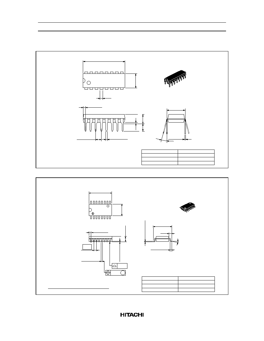
Package Dimensions
Hitachi Code
JEDEC
EIAJ
Mass (reference value)
DP-16
Conforms
Conforms
1.07 g
6.30
19.20
16
9
8
1
1.3
20.00 Max
7.40 Max
7.62
0.25
+ 0.13
≠ 0.05
2.54 ± 0.25
0.48 ± 0.10
0.51 Min
2.54 Min
5.06 Max
0∞ ≠ 15∞
1.11 Max
As of January, 2001
Unit: mm
Hitachi Code
JEDEC
EIAJ
Mass (reference value)
FP-16DA
--
Conforms
0.24 g
*Dimension including the plating thickness
Base material dimension
*0.22 ± 0.05
*0.42 ± 0.08
0.12
0.15
M
2.20 Max
5.5
10.06
0.80 Max
16
9
1
8
10.5 Max
+ 0.20
≠ 0.30
7.80
0.70 ± 0.20
0∞ ≠ 8∞
0.10 ± 0.10
1.15
1.27
0.40 ± 0.06
0.20 ± 0.04
As of January, 2001
Unit: mm

HA16141P/FP, HA16142P/FP
Rev.4, Sep. 2001, page 18 of 18
Disclaimer
1. Hitachi neither warrants nor grants licenses of any rights of Hitachi's or any third party's patent,
copyright, trademark, or other intellectual property rights for information contained in this document.
Hitachi bears no responsibility for problems that may arise with third party's rights, including
intellectual property rights, in connection with use of the information contained in this document.
2. Products and product specifications may be subject to change without notice. Confirm that you have
received the latest product standards or specifications before final design, purchase or use.
3. Hitachi makes every attempt to ensure that its products are of high quality and reliability. However,
contact Hitachi's sales office before using the product in an application that demands especially high
quality and reliability or where its failure or malfunction may directly threaten human life or cause risk
of bodily injury, such as aerospace, aeronautics, nuclear power, combustion control, transportation,
traffic, safety equipment or medical equipment for life support.
4. Design your application so that the product is used within the ranges guaranteed by Hitachi particularly
for maximum rating, operating supply voltage range, heat radiation characteristics, installation
conditions and other characteristics. Hitachi bears no responsibility for failure or damage when used
beyond the guaranteed ranges. Even within the guaranteed ranges, consider normally foreseeable
failure rates or failure modes in semiconductor devices and employ systemic measures such as fail-
safes, so that the equipment incorporating Hitachi product does not cause bodily injury, fire or other
consequential damage due to operation of the Hitachi product.
5. This product is not designed to be radiation resistant.
6. No one is permitted to reproduce or duplicate, in any form, the whole or part of this document without
written approval from Hitachi.
7. Contact Hitachi's sales office for any questions regarding this document or Hitachi semiconductor
products.
Sales Offices
Hitachi, Ltd.
Semiconductor & Integrated Circuits
Nippon Bldg., 2-6-2, Ohte-machi, Chiyoda-ku, Tokyo 100-0004, Japan
Tel: (03) 3270-2111 Fax: (03) 3270-5109
Copyright © Hitachi, Ltd., 2001. All rights reserved. Printed in Japan.
Hitachi Asia Ltd.
Hitachi Tower
16 Collyer Quay #20-00
Singapore 049318
Tel : <65>-538-6533/538-8577
Fax : <65>-538-6933/538-3877
URL : http://semiconductor.hitachi.com.sg
URL
http://www.hitachisemiconductor.com/
Hitachi Asia Ltd.
(Taipei Branch Office)
4/F, No. 167, Tun Hwa North Road
Hung-Kuo Building
Taipei (105), Taiwan
Tel : <886>-(2)-2718-3666
Fax : <886>-(2)-2718-8180
Telex : 23222 HAS-TP
URL : http://www.hitachi.com.tw
Hitachi Asia (Hong Kong) Ltd.
Group III (Electronic Components)
7/F., North Tower
World Finance Centre,
Harbour City, Canton Road
Tsim Sha Tsui, Kowloon Hong Kong
Tel : <852>-(2)-735-9218
Fax : <852>-(2)-730-0281
URL : http://semiconductor.hitachi.com.hk
Hitachi Europe GmbH
Electronic Components Group
Dornacher Straþe 3
D-85622 Feldkirchen
Postfach 201, D-85619 Feldkirchen
Germany
Tel: <49> (89) 9 9180-0
Fax: <49> (89) 9 29 30 00
Hitachi Europe Ltd.
Electronic Components Group
Whitebrook Park
Lower Cookham Road
Maidenhead
Berkshire SL6 8YA, United Kingdom
Tel: <44> (1628) 585000
Fax: <44> (1628) 585200
Hitachi Semiconductor
(America) Inc.
179 East Tasman Drive
San Jose,CA 95134
Tel: <1> (408) 433-1990
Fax: <1>(408) 433-0223
For further information write to:
Colophon 5.0

This datasheet has been download from:
www.datasheetcatalog.com
Datasheets for electronics components.