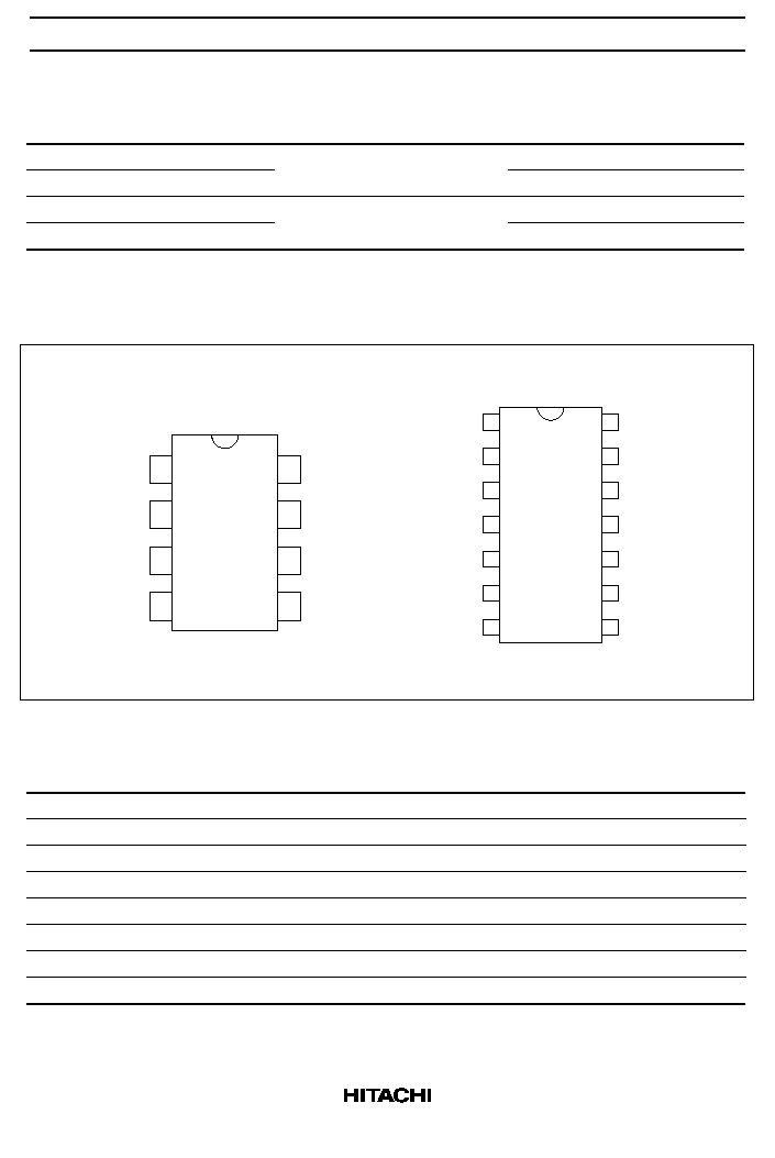
HA16654A, HA16664A Series
PWM Controlled Switching Regulator
The HA16654A and HA16664A are PWM control switching regulator ICs which drive a power MOSFET
at high speed and high frequency. The standby current is limited to as small as 1.5 mA (typ). These
devices incorporate totem pole circuits suited for high-speed push-pull operation at the output stage,
accomplishing high-speed switching with rising time t
r
= 80 ns (typ) and falling time t
f
= 40 ns (typ) at 20
V swing.
Functions
∑
Reference voltage circuit
∑
Triangular waveform oscillation circuit
∑
PWM comparator circuit
∑
Low-input malfunction protection circuit
∑
Output drive circuit
∑
Soft start and quick shut down
Features
∑
High speed switching: t
r
= 80 ns, t
f
= 40 ns (typ) when use exernal driver circuit
∑
High frequency operation:
HA16654A (f = 100 kHz to 500 kHz)
HA16664A (f = 100 kHz to 200 kHz)
Low power dissipation : 2 mA max in standby state
∑
5 V reference voltage
∑
Low-input malfunction protection (High threshold voltage: 10 V Typ, Low threshold voltage: 8 V
Typ)
∑
Adjustable dead band width
∑
Enlarged output pulse width control range (0 to 80%)
∑
Soft start and quick shut down functions
∑
Single output: totem pole

HA16654A, HA16664A Series
4
Absolute Maximum Ratings (Ta = 25∞C)
Item
Symbol
Rating
Unit
Notes
Power supply voltage
V
IN
+40
V
Collector current (Push-pull)
I
O
20
mA
Comparator input voltage
V
COM
Vref + 0.3
V
R
T
input current
I
RT
1
mA
Power dissipation
P
T
680
mW
1, 2
Operation temperature range
Topr
≠20 to +85
∞
C
Storage temperature range
Tstg
≠55 to 125
∞
C
Notes: 1. Ta
45
∞
C, if Ta > 45
∞
C, derate by 8.3 mW/
∞
C
2. Tjmax =
j≠a ∑ Pcmax + Ta (
j≠a:Thermal resistance between junction and atmosphere at set
board use)
The wiring density and the material of the set board must be chosen for thermal conductance of
efficacy board.
Electrical Characteristics
HA16654APS/AFP (Ta = 25∞C, V
IN
= 20 V, C
T
= 220 pF, R
T
= 27 k
at f 500 kHz)
Voltage Reference
Item
Symbol
Min
Typ
Max
Unit
Test Condition
Output voltage
Vref
4.75
5.00
5.25
V
Line regulation
Line
--
--
100
mV
V
IN
= 7.3 to 11 V
--
10
25
mV
V
IN
= 11 to 40 V
Load regulation
Load
--
5
16
mV
I
O
= 0 to 10 mA
Temperature stability
V
RTC
--
≠26
--
ppm/
∞
C
Short circuit current
I
OS
10
35
--
mA
Vref = 0 V