 | –≠–ª–µ–∫—Ç—Ä–æ–Ω–Ω—ã–π –∫–æ–º–ø–æ–Ω–µ–Ω—Ç: HA17080 | –°–∫–∞—á–∞—Ç—å:  PDF PDF  ZIP ZIP |

HA17080 Series
J-FET Input Operational Amplifiers
Description
Since J-FET input operational amplifiers are formed from a pair of J-FET transistors, they provide
superlative characteristics, including a high input impedance and a low input bias current. Thus they can be
used in a wide range of applications, from general-purpose control equipment to medical applications. In
particular, they are optimal for processing signals from high-impedance sensors.
Hitachi J-FET input operational amplifiers are available in single, dual, and quad versions. Other than the
HA17080, all products are internal phase compensation types and include a built-in phase compensation
capacitor. The HA17080 and the HA17083 allow offset adjustment. These products are also available in
"A" grade versions with superlative electrical characteristics to allow the selection of an operational
amplifier appropriate for the application.
Features
∑
Wide operating power supply voltage range: ±5 V to ±18 V
∑
Low input bias current: 30 pA
∑
Low input offset current: 5 pA
∑
High input impedance: 10
12
∑
High slew rate: 13 V/
µ
s
∑
Wide common mode input voltage range with operation possible near the power-supply voltage (V
CC
).
∑
High voltage gain: 106 dB
∑
The HA17080 and HA17083 support offset adjustment.
∑
Pin compatible with the Texas Instruments TL080 series.
Notes: 1. Since these products are high input impedance operational amplifiers, contamination may cause
the input bias and input offset currents to increase if they are handled with bare hands.
Avoid contamination when handling these devices.
2. Since these products provide a high slew rate, oscillation may occur due to load capacitances.
(C
L
< 100 pF: voltage follower mode)
HA17080 Series
2
Ordering Information
Type No.
Item
HA17080
HA17082
HA17083
HA17084
Number of operational amplifiers
(number of channels)
Single
Dual
Dual
Quad
Offset adjustment pin
Yes
No
Yes
No
Phase compensation type
External
Internal
Internal
Internal
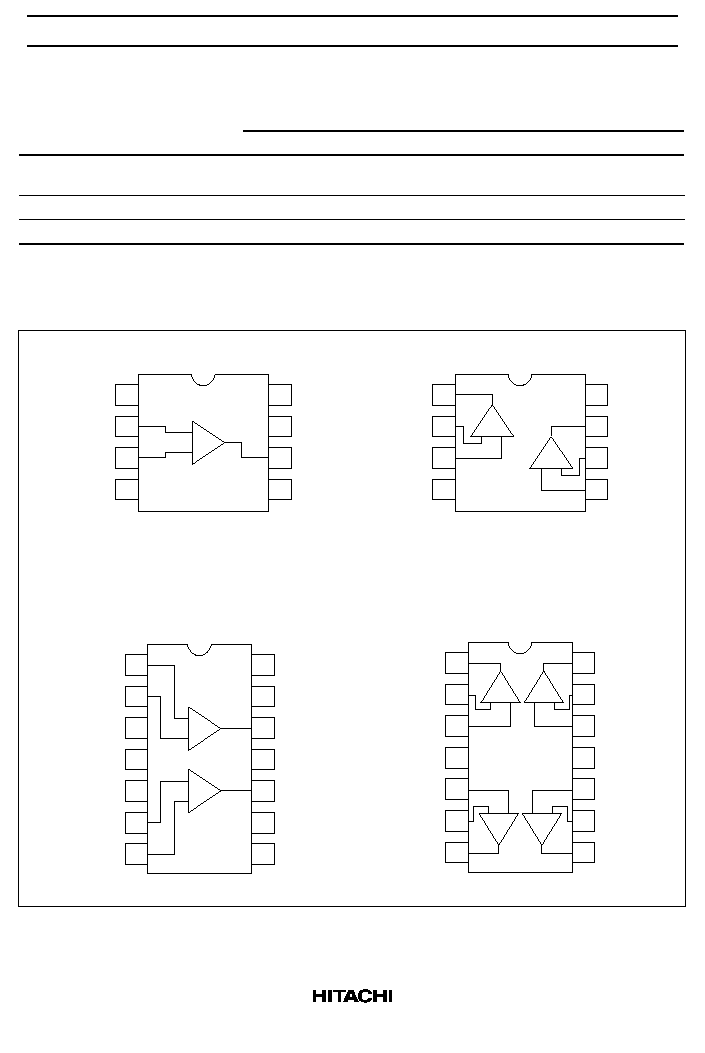
Pin Arrangement
-
+
Comp
V
CC
Vout
Offset
Null
(Top view)
Offset
Null/Comp
Vin(
-
)
Vin(+)
V
EE
1
2
3
4
8
7
6
5
HA17080
-
+
Offset
Null (N1)
V
CC
Vout1
NC
Vout2
V
CC
Offset
Null (N1)
(Top view)
Vin(
-
)1
Vin(+)1
Offset
Null (N2)
V
EE
Offset
Null (N2)
Vin(+)2
Vin(
-
)2
HA17083
-
+
1
2
1
2
3
4
5
6
7
14
13
12
11
10
9
8
(Top view)
HA17082
(Top view)
HA17084
1
-
+
+
-
1
-
+
-
+
4
2
-
+
-
+
2
3
Vout4
Vin(
-
)4
Vin(+)4
V
EE
Vin(+)3
Vin(
-
)3
Vout3
14
13
12
11
10
9
8
Vout1
Vin(
-
)1
Vin(+)1
V
CC
Vin(+)2
Vin(
-
)2
Vout2
1
2
3
4
5
6
7
Vout1
Vin(
-
)1
Vin(+)1
V
EE
1
2
3
4
V
CC
Vout2
Vin(
-
)2
Vin(+)2
8
7
6
5
HA17080 Series
3
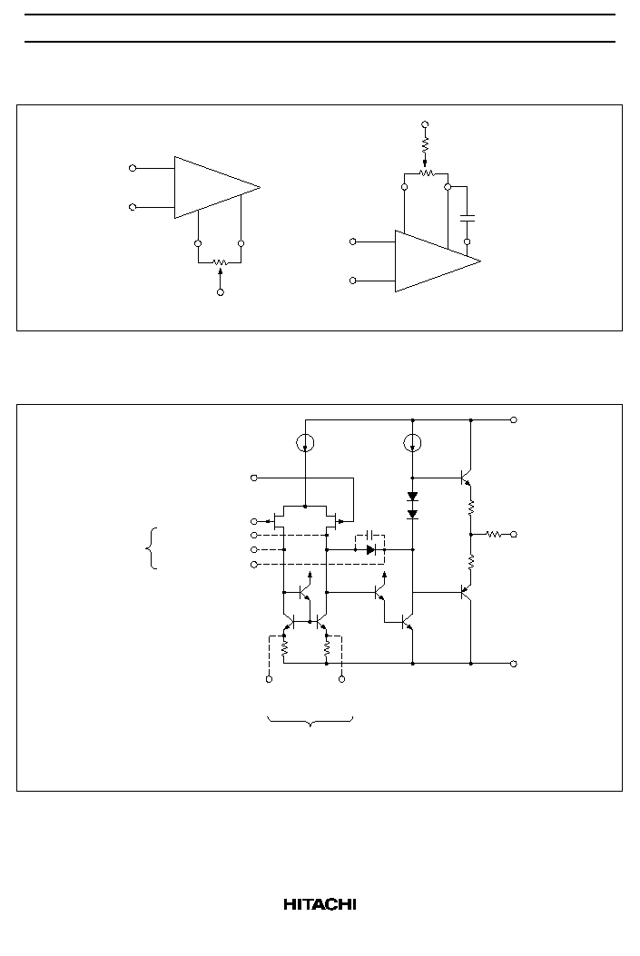
Voltage Offset Test Circuit
N2
100 K
N1
V
EE
-
+
V
CC
+
-
1 M
2 M
Offset
Null/Comp
Offset
Null
C
C
Comp
HA17080
HA17083
Circuit Structure
V
CC
Vout
V
EE
To V
CC
To V
CC
Offset
Null (N2)
Offset
Null (N1)
Vin(+)
Vin(
-
)
Offset Null/Comp
Offset Null
Comp
HA17083 only
HA17080
only
Note: The HA17080 does not have an internal phase compensation capacitor.
HA17080 Series
4
Absolute Maximum Ratings (Ta = 25∞C)
Item
Symbol
Ratings (P, PS Series)
Unit
Notes
Power-supply voltage
V
CC
+18
V
V
EE
≠18
V
Differential input voltage
Vin(diff)
±
30
V
Input voltage
Vin
±
15
V
1
Allowable power dissipation
P
T
625
mW
2
Operating temperature
Topr
≠20 to +75
∞
C
Storage temperature
Tstg
≠55 to +125
∞
C
Notes: 1. When the power-supply voltage is less than
±
15 V, the input voltage must fall within the power-
supply voltage range.
2. These are the allowable values up to Ta = 50
∞
C for the P and PS series. Derate by 8.3 mW/
∞
C
above that temperature.

HA17080 Series
5
Electrical Characteristics (V
CC
= ≠V
EE
= 15 V, Ta = 25∞C)
HA17080 Series
HA17080A Series
Item
Symbol
Min
Typ
Max
Min
Typ
Max
Unit
Test Conditions
Notes
Input offset voltage
V
IO
--
5
15
--
3
6
mV
R
S
= 50
1
Input offset current
I
IO
--
5
200
--
5
100
pA
I
IO
=
|
I
IB(+)
≠ I
IB(≠)
|
1
Input bias current
I
IB
--
30
400
--
30
200
pA
1, 2
Common-mode
input voltage range
V
CM
±
10
--
--
±
11
--
--
V
1
Maximum output
voltage amplitude
Vop-p
24
27
--
24
27
--
V
R
L
10 k
20
24
--
20
24
--
R
L
2 k
Voltage Gain
A
VD
88
106
--
94
106
--
dB
R
L
2 k
, V
O
=
±
10 V
1
Common-mode
rejection ratio
CMR
70
86
--
80
86
--
dB
R
S
10 k
1
Power supply
rejection ratio
PSRR
70
86
--
80
86
--
dB
R
S
10 k
1
Supply current
I
CC
--
1.4
2.8
--
1.4
2.8
mA
3
Bandwidth
BW
--
3
--
--
3
--
MHz
A
VD
= 1
Slew rate
SR
--
13
--
--
13
--
V/
µ
s
Vin = 10 V, R
L
= 2 k
,
C
L
= 100 pF, A
VD
= 1
Channel separation
CS
--
120
--
--
120
--
dB
A
VD
= 100
Rise time
t
r
--
0.1
--
--
0.1
--
µ
s
Vin = 20 mV, R
L
= 2 k
Overshoot
Vover
--
10
--
--
10
--
%
C
L
= 100 pF, A
VD
= 1
Input resistance
Rin
--
10
12
--
--
10
12
--
Input noise voltage
Vn
--
35
--
--
35
--
nV/
Hz
R
S
= 100
, f = 1 kHz
Notes: 1. The non-A ratings apply to the HA17080, HA17082, HA17083, and HA17084.
The A version ratings apply to the HA17080A, HA17082A, HA17083A, and HA17084A.
2. This is the J-FET gate leakage current, which is temperature dependent. The junction
temperature must be held near room temperature when measuring this parameter.
3. This is the per-channel value.
HA17080 Series
6
Characteristic Curves
-
50
-
25
0
25
50
75
100
10 k
1 k
100
10
-
10
-
5
0
5
10
120
100
80
60
40
20
0
-
50
-
25
0
50
100
30
25
20
15
10
5
0
25
75
100
1 k
10 k
1 M
10 M
30
25
20
15
10
5
0
100 k
V
CC
= +15 V
V
EE
=
-
15 V
Ta = 25
∞
C
V
CC
= +15 V
V
EE
=
-
15 V
2 k
R
L
= 10 k
V
CC
= +15 V
V
EE
=
-
15 V
V
CM
= 0 V
R
L
= 10 k
2 k
V
CC
= +15 V
V
EE
=
-
15 V
Ta = 25
∞
C
0
±
3
±
6
±
12
±
18
30
25
20
15
10
5
0
Power-supply voltage V
CC
, V
EE
(V)
±
9
±
15
0.1
0.2
0.5
2
10
30
25
20
15
10
5
0
Load resistance R
L
(k
)
1.0
5
R
L
= 10 k
Ta = 25
∞
C
V
CC
= +15 V
V
EE
=
-
15 V
Ta = 25
∞
C
Common-mode input voltage V
CM
(V)
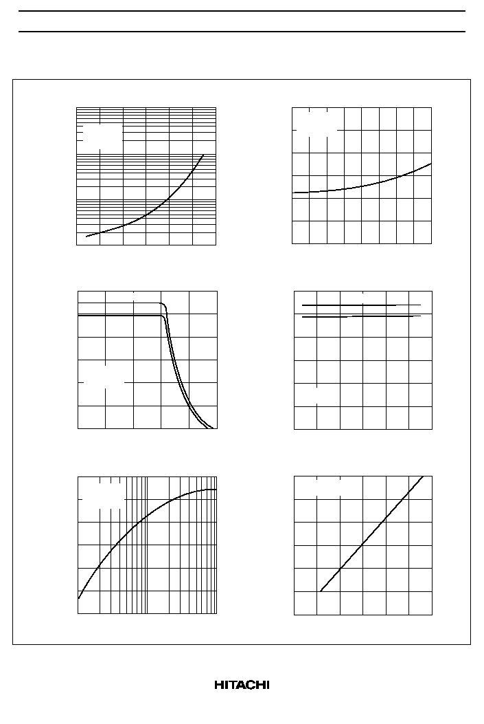
Input Bias Current vs.
Common-Mode Input Voltage
Maximum output voltage amplitude
V
OP-P
(V)
Maximum output voltage amplitude
V
OP-P
(V)
Maximum output voltage amplitude
V
OP-P
(V)
Maximum output voltage amplitude
V
OP-P
(V)
Ambient temperature Ta (
∞
C)
Maximum Output Voltage
Amplitude vs. Ambient Temperature
Frequency f (Hz)
Maximum Output Voltage
Amplitude vs. Frequency
Maximum Output Voltage
Amplitude vs. Load Resistance
Maximum Output Voltage
Amplitude vs. Power-Supply Voltage
Input bias current I
IB
(pA)
Input bias current I
IB
(pA)
Ambient temperature Ta (
∞
C)
Input Bias Current vs.
Ambient Temperature

HA17080 Series
7
1
10
100
1 k
10 k
150
125
100
75
50
25
0
Frequency f (Hz)
Frequency f (Hz)
Frequency f (Hz)
Frequency f (Hz)
Frequency f (Hz)
150
125
100
75
50
25
0
100 k 1 M 10 M
10
100
1 k
10 k
100 k
1 M
10 M
V
CC
= +15 V
V
EE
=
-
15 V
R
L
= 10 k
Ta = 25
∞
C
V
CC
= +15 V
V
EE
=
-
15 V
C
L
= 3 pF
Ta = 25
∞
C
-
50
-
25
0
25
50
150
125
100
75
50
25
0
75
100
10
100
1 k
10 k
100 k
120
100
80
60
40
20
0
1 M
10 M
10
100
1 k
10 k
100 k
120
100
80
60
40
20
0
1 M
10 M
10
100
1 k
10 k
100 k
120
100
80
60
40
20
0
Input noise voltage Vn (nV/
Hz
)
V
CC
= +15 V
V
EE
=
-
15 V
R
S
= 100
Ta = 25
∞
C
V
CC
= +15 V
V
EE
=
-
15 V
Ta = 25
∞
C
V
CC
= +15 V
V
EE
=
-
15 V
Ta = 25
∞
C
V
CC
= +15 V
V
EE
=
-
15 V
R
L
= 2 k
V
CC
V
EE
Voltage gain A
VD
(dB)
Voltage gain A
VD
(dB)
Voltage gain A
VD
(dB)
Voltage Gain vs. Frequency (1)
Voltage Gain vs. Frequency (2)
Ambient temperature Ta (
∞
C)
Voltage Gain vs.
Ambient Temperature
Common-mode rejection ratio
CMR (dB)
Common-Mode Rejection Ratio vs.
Frequency
Power-supply rejection ratio
PSRR (dB)
Power-Supply Rejection Ratio vs.
Frequency
Input Noise Voltage vs.
Frequency

HA17080 Series
8
0
±
3
±
18
2.4
2.0
1.6
1.2
0.8
0.4
0
±
6
±
9
±
12
±
15
-
50
-
25
100
2.4
2.0
1.6
1.2
0.8
0.4
0
0
25
50
75
-
50
-
25
100
120
100
80
60
40
20
0
0
25
50
75
0
±
3
±
18
100
80
60
40
20
0
±
6
±
9
±
12
±
15
V
CC
= +15 V
V
EE
=
-
15 V
No signal
No load
Per channel
V
CC
= +15 V
V
EE
= ≠15 V
Per channel
Ta = 25
∞
C
No signal
No load
Ta = 25
∞
C
No signal
No load
0
0.5
3
6
4
2
0
-
2
-
4
-
6
Output Voltage Vout (V)
Output Voltage Vout (V)
1
1.5
2
2.5
0
100
+2.0
+1.0
0
-
1.0
-
2.0
50
3.5
V
CC
= +15 V
V
EE
=
-
15 V
R
S
= 51
Rf = 5.1 k
R = 100 k
V
CC
= +15 V
V
EE
=
-
15 V
R
L
= 2 k
C
L
= 100 pF
Ta = 25
∞
C
Input
Output
Supply current I
CC
±
(mA)
Supply current I
CC
±
(mA)
Power-supply voltage V
CC
, V
EE
(V)
Power-supply voltage V
CC
, V
EE
(V)
Supply current vs.
Power-Supply Voltage
Ambient temperature Ta (
∞
C)
Ambient temperature Ta (
∞
C)
Supply current vs.
Ambient Temperature
Power Dissipation vs.
Ambient Temperature
Power Dissipation vs.
Power-Supply Voltage
Power dissipation Pd (mW)
Power dissipation Pd (mW)
Time t (
µ
s)
Voltage Follower Large Signa
Pulse Response
Resistor position a (%)
HA17083 Offset Adjustment

HA17080 Series
9
Package Dimensions
Hitachi Code
JEDEC
EIAJ
Mass (reference value)
DP-8
Conforms
Conforms
0.54 g
Unit: mm
1
4
5
8
9.6
10.6 Max
0.89
1.3
6.3
7.4 Max
2.54 Min
5.06 Max
2.54
±
0.25
0.48
±
0.10
7.62
0.25
+ 0.10
≠ 0.05
0
∞
≠ 15
∞
0.1 Min
1.27 Max
Hitachi Code
JEDEC
EIAJ
Mass (reference value)
DP-14
Conforms
Conforms
0.97 g
Unit: mm
7.62
0.25
0
∞
≠ 15
∞
19.20
20.32 Max
1
8
14
7
1.30
2.54
±
0.25
0.48
±
0.10
6.30
7.40 Max
0.51 Min
2.54 Min
5.06 Max
+ 0.10
≠ 0.05
2.39 Max

HA17080 Series
10
Cautions
1. Hitachi neither warrants nor grants licenses of any rights of Hitachi's or any third party's patent,
copyright, trademark, or other intellectual property rights for information contained in this document.
Hitachi bears no responsibility for problems that may arise with third party's rights, including
intellectual property rights, in connection with use of the information contained in this document.
2. Products and product specifications may be subject to change without notice. Confirm that you have
received the latest product standards or specifications before final design, purchase or use.
3. Hitachi makes every attempt to ensure that its products are of high quality and reliability. However,
contact Hitachi's sales office before using the product in an application that demands especially high
quality and reliability or where its failure or malfunction may directly threaten human life or cause risk
of bodily injury, such as aerospace, aeronautics, nuclear power, combustion control, transportation,
traffic, safety equipment or medical equipment for life support.
4. Design your application so that the product is used within the ranges guaranteed by Hitachi particularly
for maximum rating, operating supply voltage range, heat radiation characteristics, installation
conditions and other characteristics. Hitachi bears no responsibility for failure or damage when used
beyond the guaranteed ranges. Even within the guaranteed ranges, consider normally foreseeable
failure rates or failure modes in semiconductor devices and employ systemic measures such as fail-
safes, so that the equipment incorporating Hitachi product does not cause bodily injury, fire or other
consequential damage due to operation of the Hitachi product.
5. This product is not designed to be radiation resistant.
6. No one is permitted to reproduce or duplicate, in any form, the whole or part of this document without
written approval from Hitachi.
7. Contact Hitachi's sales office for any questions regarding this document or Hitachi semiconductor
products.
Hitachi, Ltd.
Semiconductor & Integrated Circuits.
Nippon Bldg., 2-6-2, Ohte-machi, Chiyoda-ku, Tokyo 100-0004, Japan
Tel: Tokyo (03) 3270-2111 Fax: (03) 3270-5109
Copyright ' Hitachi, Ltd., 1998. All rights reserved. Printed in Japan.
Hitachi Asia Pte. Ltd.
16 Collyer Quay #20-00
Hitachi Tower
Singapore 049318
Tel: 535-2100
Fax: 535-1533
URL
NorthAmerica
: http:semiconductor.hitachi.com/
Europe
: http://www.hitachi-eu.com/hel/ecg
Asia (Singapore)
: http://www.has.hitachi.com.sg/grp3/sicd/index.htm
Asia (Taiwan)
: http://www.hitachi.com.tw/E/Product/SICD_Frame.htm
Asia (HongKong)
: http://www.hitachi.com.hk/eng/bo/grp3/index.htm
Japan
: http://www.hitachi.co.jp/Sicd/indx.htm
Hitachi Asia Ltd.
Taipei Branch Office
3F, Hung Kuo Building. No.167,
Tun-Hwa North Road, Taipei (105)
Tel: <886> (2) 2718-3666
Fax: <886> (2) 2718-8180
Hitachi Asia (Hong Kong) Ltd.
Group III (Electronic Components)
7/F., North Tower, World Finance Centre,
Harbour City, Canton Road, Tsim Sha Tsui,
Kowloon, Hong Kong
Tel: <852> (2) 735 9218
Fax: <852> (2) 730 0281
Telex: 40815 HITEC HX
Hitachi Europe Ltd.
Electronic Components Group.
Whitebrook Park
Lower Cookham Road
Maidenhead
Berkshire SL6 8YA, United Kingdom
Tel: <44> (1628) 585000
Fax: <44> (1628) 778322
Hitachi Europe GmbH
Electronic components Group
Dornacher Stra
e 3
D-85622 Feldkirchen, Munich
Germany
Tel: <49> (89) 9 9180-0
Fax: <49> (89) 9 29 30 00
Hitachi Semiconductor
(America) Inc.
179 East Tasman Drive,
San Jose,CA 95134
Tel: <1> (408) 433-1990
Fax: <1>(408) 433-0223
For further information write to: