HA17324/A Series
Quad Operational Amplifier
ADE-204-031 (Z)
1st Edition
Apr. 2000
Description
HA17324 series and HA17324A series are quad operational amplifier that provide high gain and internal
phase compensation, with single power supply. They can be widely used to control equipments.
Features
∑
Wide range of supply voltage, and single power supply used
∑
Internal phase compensation
∑
Wide range of common mode voltage, and possible to operate with an input about 0V
Features only for "A" series
∑
Low electro-magnetic interference level
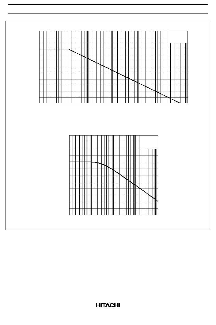
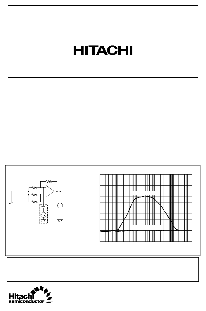
Output Offset Voltage vs. Input Interference
Measurement Condition
Output offset voltage
(arb. unit)
5.0
4.0
3.0
2.0
1.0
0
-
1.0
100E+3
1E+6
10E+6
100E+6
1E+9
10E+9
Input RF frequency (Hz)
HA17324A series
HA17324 series
Rs
-
+
Rs
0.01
µ
Vin
-
10 dBm
RF signal source
(for quasi-RF noise)
Vcc = +7.5 V
Vee =
-
7.5 V
Rf
Rf
Vout
(= 100
Vio)
V
_
Notice: The example of an applied circuit or combination with other equipment shown herein indicates
characteristics and performance of semiconductor -applied products.
The company shall assume no responsibility for any problem involving a patent caused when
applying the descriptions in the example.

HA17324/A Series
4
Absolute Maximum Ratings (Ta = 25
∞
C)
Ratings
Item
Symbol
HA17324/P/AP
HA17324F/FP/ARP/AFP
Unit
Supply voltage
V
CC
32
32
V
Sink current
Isink
50
50
mA
Power dissipation
P
T
625 *
1
625 *
2
mW
Common mode input voltage
V
CM
≠0.3 to V
CC
≠0.3 to V
CC
V
Differential input voltage
Vin (diff)
±
V
CC
±
V
CC
V
Operating temperature
Topr
≠20 to +75
≠20 to +75
∞
C
Storage temperature
Tstg
≠55 to +125
≠55 to +125
∞
C
Notes: 1. This is the allowable values up to Ta = 50
∞
C. Derate by 8.3 mW/
∞
C.
2. Tjmax =
j-a ∑ P
C
max + Ta (
j-a; Thermal resistor between junction and ambient at set board
use).
The wiring density and the material of the set board must be chosen for thermal conductance of
efficacy board.
And P
C
max cannot be over the value of P
T
.
240
220
200
180
160
140
120
100
80
Thermal resistor
j-a
(
∞
C)
0.5
1
2
5
10
20
Thermal conductance of efficacy board (W/m
∞
C)
a
b
SOP14
-
with compound
SOP14
-
no compound
40 mm
a. Class epoxy board of 10% wiring density
b. Class epoxy board of 30% wiring density
1.5 t epoxy

HA17324/A Series
11
Cautions
1. Hitachi neither warrants nor grants licenses of any rights of Hitachi's or any third party's patent,
copyright, trademark, or other intellectual property rights for information contained in this document.
Hitachi bears no responsibility for problems that may arise with third party's rights, including
intellectual property rights, in connection with use of the information contained in this document.
2. Products and product specifications may be subject to change without notice. Confirm that you have
received the latest product standards or specifications before final design, purchase or use.
3. Hitachi makes every attempt to ensure that its products are of high quality and reliability. However,
contact Hitachi's sales office before using the product in an application that demands especially high
quality and reliability or where its failure or malfunction may directly threaten human life or cause risk
of bodily injury, such as aerospace, aeronautics, nuclear power, combustion control, transportation,
traffic, safety equipment or medical equipment for life support.
4. Design your application so that the product is used within the ranges guaranteed by Hitachi particularly
for maximum rating, operating supply voltage range, heat radiation characteristics, installation
conditions and other characteristics. Hitachi bears no responsibility for failure or damage when used
beyond the guaranteed ranges. Even within the guaranteed ranges, consider normally foreseeable
failure rates or failure modes in semiconductor devices and employ systemic measures such as fail-
safes, so that the equipment incorporating Hitachi product does not cause bodily injury, fire or other
consequential damage due to operation of the Hitachi product.
5. This product is not designed to be radiation resistant.
6. No one is permitted to reproduce or duplicate, in any form, the whole or part of this document without
written approval from Hitachi.
7. Contact Hitachi's sales office for any questions regarding this document or Hitachi semiconductor
products.
Hitachi, Ltd.
Semiconductor & Integrated Circuits.
Nippon Bldg., 2-6-2, Ohte-machi, Chiyoda-ku, Tokyo 100-0004, Japan
Tel: Tokyo (03) 3270-2111 Fax: (03) 3270-5109
Copyright ' Hitachi, Ltd., 2000. All rights reserved. Printed in Japan.
Hitachi Asia Pte. Ltd.
16 Collyer Quay #20-00
Hitachi Tower
Singapore 049318
Tel: 535-2100
Fax: 535-1533
URL
NorthAmerica
: http:semiconductor.hitachi.com/
Europe
: http://www.hitachi-eu.com/hel/ecg
Asia (Singapore)
: http://www.has.hitachi.com.sg/grp3/sicd/index.htm
Asia (Taiwan)
: http://www.hitachi.com.tw/E/Product/SICD_Frame.htm
Asia (HongKong)
: http://www.hitachi.com.hk/eng/bo/grp3/index.htm
Japan
: http://www.hitachi.co.jp/Sicd/indx.htm
Hitachi Asia Ltd.
Taipei Branch Office
3F, Hung Kuo Building. No.167,
Tun-Hwa North Road, Taipei (105)
Tel: <886> (2) 2718-3666
Fax: <886> (2) 2718-8180
Hitachi Asia (Hong Kong) Ltd.
Group III (Electronic Components)
7/F., North Tower, World Finance Centre,
Harbour City, Canton Road, Tsim Sha Tsui,
Kowloon, Hong Kong
Tel: <852> (2) 735 9218
Fax: <852> (2) 730 0281
Telex: 40815 HITEC HX
Hitachi Europe Ltd.
Electronic Components Group.
Whitebrook Park
Lower Cookham Road
Maidenhead
Berkshire SL6 8YA, United Kingdom
Tel: <44> (1628) 585000
Fax: <44> (1628) 778322
Hitachi Europe GmbH
Electronic components Group
Dornacher Stra
e 3
D-85622 Feldkirchen, Munich
Germany
Tel: <49> (89) 9 9180-0
Fax: <49> (89) 9 29 30 00
Hitachi Semiconductor
(America) Inc.
179 East Tasman Drive,
San Jose,CA 95134
Tel: <1> (408) 433-1990
Fax: <1>(408) 433-0223
For further information write to: