 | –≠–ª–µ–∫—Ç—Ä–æ–Ω–Ω—ã–π –∫–æ–º–ø–æ–Ω–µ–Ω—Ç: HA17358A | –°–∫–∞—á–∞—Ç—å:  PDF PDF  ZIP ZIP |
HA17358/A Series
Dual Operational Amplifier
ADE-204-033A (Z)
Rev. 1
Mar. 2001
Description
HA17358 series and HA17358A series are dual operational amplifier that provide high gain and internal
phase compensation, with single power supply. They can be widely applied to control equipments and to
general use.
Features
∑
Wide range of supply voltage, and single power supply used
∑
Wide range of common mode voltage, and possible to operate with an input about 0 V, and output
around 0 V is available
∑
Frequency characteristics and input bias current are temperature compensated
Features only for "A" series
∑
Low electro-magnetic susceptibility level
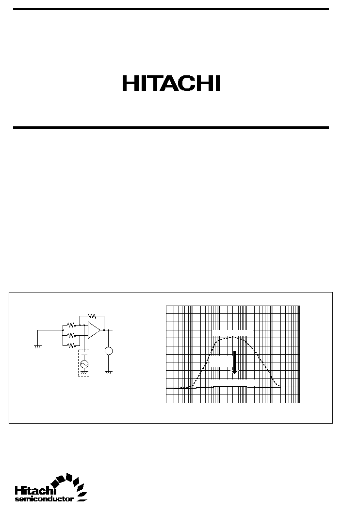
Output Offset Voltage vs. Input Interference
Measurement Condition
Output offset voltage
(arb. unit)
5.0
4.0
3.0
2.0
1.0
0
-
1.0
100E+3
1E+6
10E+6
100E+6
1E+9
10E+9
Input RF frequency (Hz)
HA17358A series
HA17358 series
Rs
-
+
Rs
0.01
µ
Vin
-
10 dBm
RF signal source
(for quasi-RF noise)
Vcc = +7.5 V
Vee =
-
7.5 V
Rf
Rf
Vout
(= 100
Vio)
V
_
Improve-
ment

HA17358/A Series
2
Ordering Information
Type No.
Application
Package
HA17358
Commercial use
DP-8B
HA17358F
FP-8D
HA17358APS
Industrial use
DP-8B
HA17358ARP
Commercial use
FP-8DC
HA17358AFP
FP-8D
Pin Arrangement
-
+
Vout1
Vin(
-
)1
Vin(+)1
GND
V
CC
Vout2
Vin(
-
)2
Vin(+)2
+
-
8
7
6
5
1
2
3
4
(Top View)
1
2
Circuit Schematic (1/2)
Q
1
Q
4
Q
2
Q
3
Q
5
Q
6
Q
7
Q
13
Q
12
Q
11
Q
10
Q
8
Q
9
Vout
R
1
Vin(+)
Vin(
-
)
C

HA17358/A Series
3
Absolute Maximum Ratings (Ta = 25
∞
C)
Ratings
Item
Symbol
HA17358
HA17358F
HA17358APS
HA17358AFP/ARP
Unit
Supply voltage
V
CC
32
32
32
32
V
Sink current
Isink
50
50
50
50
mA
Power dissipation
P
T
570 *
1
385 *
2
570 *
1
385 *
2
mW
Common mode
input voltage
V
CM
-
0.3 to V
CC
-
0.3 to V
CC
-
0.3 to V
CC
-
0.3 to V
CC
V
Differential input
voltage
Vin (diff)
±
V
CC
±
V
CC
±
V
CC
±
V
CC
V
Operating
temperature
Topr
-
20 to +75
-
20 to +75
-
40 to +85
-
40 to +85
∞
C
Storage
temperature
Tstg
-
55 to +125
-
55 to +125
-
55 to +125
-
55 to +125
∞
C
Notes: 1. This is the allowable values up to Ta = 50
∞
C. Derate by 8.3 mW/
∞
C.
2. These are the allowable values up to Ta = 25
∞
C mounting in air.
When it is mounted on glass epoxy board of 40 mm
◊
40 mm
◊
1.5 mmt with 30% wiring density,
the allowable value is 570 mW up to Ta = 45
∞
C. If Ta > 45
∞
C, derate by 7.14 mW/
∞
C.

HA17358/A Series
4
Electrical Characteristics (V
CC
= +15 V, Ta = 25
∞
C)
Item
Symbol
Min
Typ
Max
Unit
Test Conditions
Input offset voltage
V
IO
--
3
7
mV
V
CM
= 7.5V, R
S
= 50
, Rf = 50k
Input offset current
I
IO
--
5
50
nA
V
CM
= 7.5V, I
IO
=
|
I
I (+)
≠ I
I (≠)
|
Input bias current
I
IB
--
30
250
nA
V
CM
= 7.5V
Power source rejection
ratio
PSRR
--
93
--
dB
R
S
= 1k
, Rf = 100k
Voltage gain
A
VD
75
90
--
dB
R
L
=
, R
S
= 1k
, Rf = 100k
Common mode rejection
ratio
CMR
--
80
--
dB
R
S
= 50
, Rf = 5k
Common mode input
voltage range
V
CM (+)
13.5
--
--
V
R
S
= 1k
, Rf = 100k
V
CM (≠)
--
--
≠0.3
V
R
S
= 1k
, Rf = 100k
Peak-to-peak output
voltage
Vop-p
--
13.6
--
V
f = 100Hz, R
L
= 20k
, R
S
= 1k
,
Rf = 100k
Output source current
Iosource
20
40
--
mA
V
IN
+
= 1V, V
IN
≠
= 0V, V
OH
= 10V
Output sink current
Iosink
10
20
--
mA
V
IN
≠
= 1V, V
IN
+
= 0V, V
OL
= 2.5V
Output sink current
Iosink
15
50
--
µ
A
V
IN
≠
= 1V, V
IN
+
= 0V,
Vout = 200mV
Supply current
I
CC
--
0.8
2
mA
V
IN
= GND, R
L
=
Slew rate
SR
--
0.2
--
V/
µ
s
R
L
=
, V
CM
= 7.5V, f = 1.5kHz
Channel separation
CS
--
120
--
dB
f = 1kHz

HA17358/A Series
5
Characteristic Curves
Output Source Current vs. Ambient Temperature
80
Output source current Iosource (mA)
Ambeint temperature Ta (
∞
C)
70
60
50
40
30
20
10
0
-
20
0
20
40
60
80
V
CC
= 15 V
V
OH
= 10 V
Input Bias Current vs. Ambient Temperature
80
Input bias current I
IB
(nA)
Ambeint temperature Ta (
∞
C)
70
60
50
40
30
20
10
0
-
20
0
20
40
60
80
V
CC
= 15 V
V
CM
= 7.5 V
Supply Current vs. Supply Voltage
4
Supply current I
CC
(mA)
Supply voltage V
CC
(V)
3
2
1
0
8
16
24
32
40
Ta = 25
∞
C
80
Input bias current I
IB
(nA)
Supply voltage V
CC
(V)
60
40
20
0
8
16
24
32
40
Ta = 25
∞
C
Voltage Gain vs. Supply Voltage
160
Voltage gain A
VD
(dB)
Supply voltage V
CC
(V)
120
80
40
0
8
16
24
32
40
Ta = 25
∞
C
R
L
=
Maxlmum Output Voltage vs. Frequency
Input Bias Current vs. Supply Voltage
20
Maximum output voltage V
OP
-
P
(V)
Frequency f (Hz)
1 k
3 k
10 k
30 k
100 k 300 k
16
12
8
4
0
V
CC
= 15 V
Ta = 25
∞
C
R
L
= 20 k
1 M