
HA17384SPS/SRP, HA17384HPS/HRP,
HA17385HPS/HRP
High Speed Current Mode PWM Control IC
for Switching Power Supply
ADE-204-028A (Z)
2nd Edition
Nov. 1999
Description
The HA17384S/H and HA17385H are PWM control switching regulator IC series suitable for highspeed,
current-mode switching power supplies. With ICs from this series and a few external parts, a small, low
cost flyback-transformer switching power supply can be constructed, which facilitates good line regulation
by current mode control. Synchronous operation driven after an external signal can also be easily obtained
which offers various applications such as a power supply for monitors small multi-output power supply.
The IC series are composed of circuits required for a switching regulator IC. That is a under-voltage
lockout (UVL), a high precision reference voltage regulator (5.0 V ± 2%), a triangular wave oscillator for
timing generation, a high-gain error amplifier, and as totem pole output driver circuit which directly drives
the gate of power MOSFETs found in main switching devices. In addition, a pulse-by-pulse type, high-
speed, current-detection comparator circuit with variable detection level is incorporated which is required
for current mode control.
The HA17384SPS includes the above basic function circuits. In addition to these basic functions, the H
Series incorporates thermal shut-down protection (TSD) and overvoltage protection (OVP) functions, for
configuration of switching power supplies that meet the demand for high safety levels.
Between the HA17384 and HA17385, only the UVL threshold voltages differ as shown in the product
lineup table.(See next page.)
This IC is pin compatible with the "3842 family" ICs made by other companies in the electronics industry.
However, due to the characteristics of linear ICs, it is not possible to achieve ICs that offer full
compatibility in every detail.
Therefore, when using one of these ICs to replace another manufacturer's IC, it must be recognized that it
has different electrical characteristics, and it is necessary to confirm that there is no problem with the power
supply (mounting) set used.

HA17384SPS/SRP, HA17384HPS/HRP, HA17385HPS/HRP
2
Functions
∑
Under-voltage lockout system
∑
Reference voltage regulator of 5.0 V ± 2%
∑
Triangular wave (sawtooth) oscillator
∑
Error amplifier
∑
Totem pole output driver circuit (direct driving for power MOSFETs)
∑
Current-detection comparator circuit for current mode
∑
OVP function (over voltage protection) *
1
∑
TSD function (thermal shut-down protection) *
1
∑
Protect function by zener diode (between power input and GND)
Note: 1. H series only.
Features
∑
High-safety UVL circuit is used (Both V
IN
and Vref are monitored)
∑
High speed operation:
Current detection response time: 100 ns Typ
Maximum oscillation frequency: 500 kHz
∑
Low standby current: 170
µ
A Typ
∑
Wide range dead band time
(Discharge current of timing capacitance is constant 8.4 mA Typ)
∑
Able to drive power MOSFET directly
(Absolute maximum rating of output current is ±1 A peak)
∑
OVP function (over voltage protection) is included *
1
(Output stops when FB terminal voltage is 7.0 V Typ or higher)
∑
TSD function (thermal shut-down protection) is included *
1
(Output stops when the temperature is 160∞C Typ or higher)
∑
Zener protection is included
(Clamp voltage between V
IN
and GND is 34 V Typ)
∑
Wide operating temperature range:
Operating temperature: ≠20∞C to +105∞C
Junction temperature: 150∞C *
2
Note: 1. H series only.
2. S series only.
HA17384SPS/SRP, HA17384HPS/HRP, HA17385HPS/HRP
3
Product Line-up
Package
Additional Function
UVL Power Supply
Threshold Voltage
DILP8 (DP-8)
SOP8 (FP-8DC)
TSD
(Thermal shut-
down protection)
OVP
(Over voltage
protection)
V
TH UVL
(V) Typ
V
TL UVL
(V) Typ
HA17384SPS
HA17384SRP
--
--
16.0
10.0
HA17384HPS
HA17384HRP
r
r
HA17385HPS
HA17385HRP
r
r
8.4
7.6
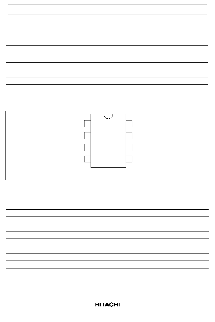
Pin Arrangement
1
2
3
4
8
7
6
5
COMP
FB
CS
R
T
/C
T
Vref
V
IN
OUT
GND
(Top view)
Pin Function
Pin No.
Symbol
Function
Note
1
COMP
Error amplifier output pin
2
FB
Inverting input of error amp./OVP input pin
1
3
CS
Current sensing signal input pin
4
R
T
/C
T
Timing resistance, timing capacitance connect pin
5
GND
Groung pin
6
OUT
PWM Pulse output pin
7
V
IN
Power supply voltage input pin
8
Vref
Reference voltage 5V output pin
Note:
1. Overvoltage protection (OVP) input is usable only for the HA17384H and HA17385H.
HA17384SPS/SRP, HA17384HPS/HRP, HA17385HPS/HRP
4
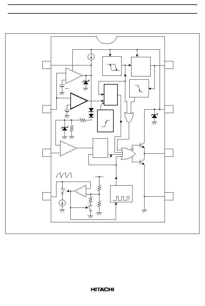
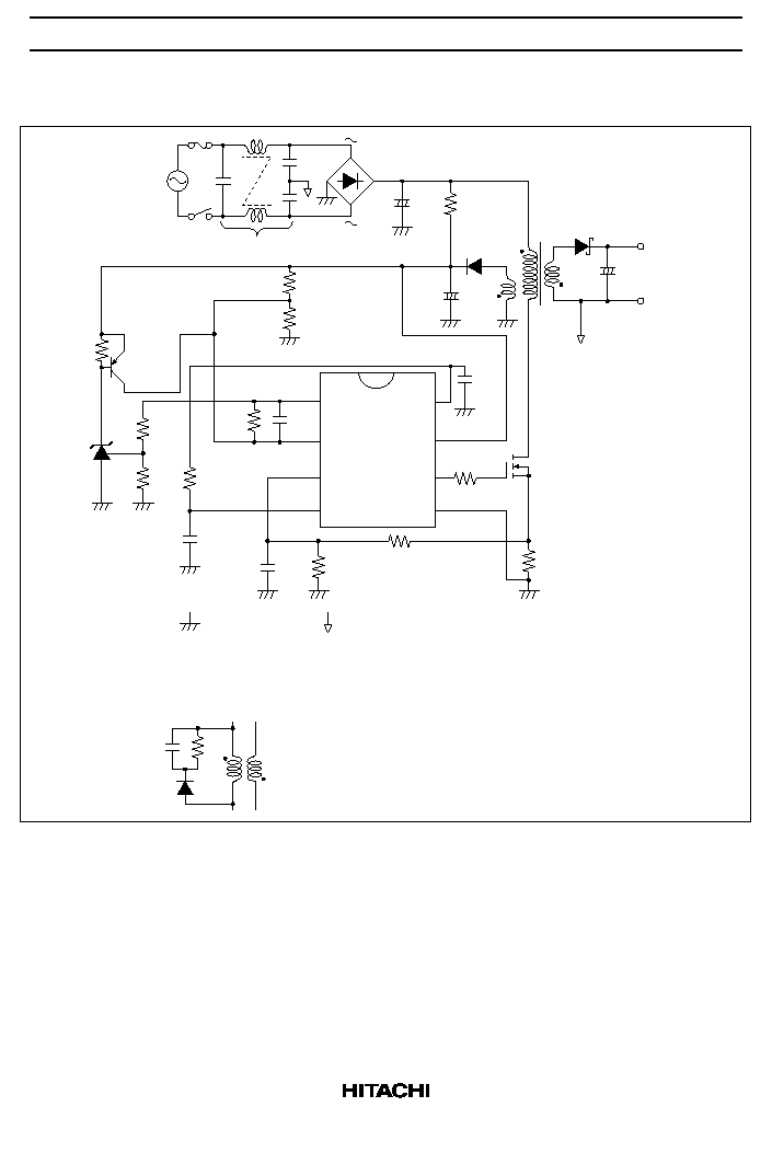
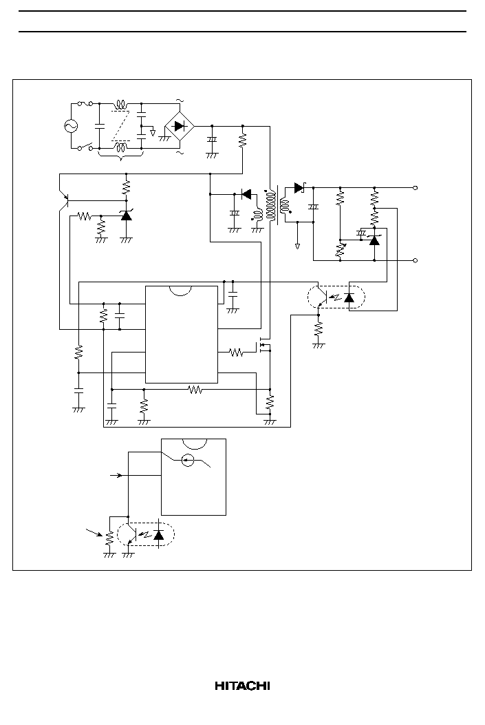
Block Diagram
Oscillator
Totem pole
output circuit
Note: 1. Blocks with bold line are not included in HA17384SPS/SRP.
0.8mA
EA
-
+
OVP
-
+
CS
-
+
7.0V
UVL1
H
L
VL VH
UVL2
Vref > 4.7V
R
Q
S
6.5V
1
2
Vref
(2.5V)
*
1
2V
F
160
∞
C
2R
R
1V
R
S
Q
PWM LOGIC
Vref
NOR
8.4 mA
1.2V
+
-
OR
34V
1
2
3
4
8
7
6
COMP
FB
(OVP input)
CS
RT/CT
Vref
V
IN
OUT
5
GND
2.8 V
OUT
5V band
gap
reference
regulator
OVP
latch
TSD
sense
CS
latch
Latch set
pulse
HA17384SPS/SRP, HA17384HPS/HRP, HA17385HPS/HRP
5
Absolute Maximum Ratings
Item
Symbol
Rating
Unit
Note
Supply voltage
V
IN
30
V
DC output current
I
O
±
0.1
A
Peak output current
I
O PEAK
±
1.0
A
Error amplifier input voltage
V
FB
≠0.3 to V
IN
V
COMP terminal input voltage
V
COMP
≠0.3 to +7.5
V
Error output sink current
I
OEA
10
mA
Power dissipation
P
T
680
mW
1, 2
Operating temperature
Topr
≠20 to +105
∞
C
Junction temperature
Tj
125
∞
C
3
150
∞
C
4
Storage temperature
Tstg
≠55 to +125
∞
C
3
≠55 to +150
∞
C
4
Notes: 1. For the HA17384HPS and HA17385HPS,
This value applies up to Ta = 43
∞
C; at temperatures above this, 8.3 mW/
∞
C derating should be
applied.
For the HA17384SPS,
This value applies up to Ta = 68
∞
C; at temperatures above this, 8.3 mW/
∞
C derating should be
applied.
Power Dissipation P
T
(mW)
Ambient Temperature Ta (
∞
C)
680mW
374mW
43
∞
C
68
∞
C
150
∞
C
800
600
400
200
0
-
20
0
20
40
60
80
100
120
140
160
166mW
105
∞
C
125
∞
C
HA17384SPS
HA17384HPS, HA17385HPS
HA17384SPS/SRP, HA17384HPS/HRP, HA17385HPS/HRP
6
Absolute Maximum Ratings (cont)
Notes: 2. This is the value when the device is mou nted on a glass-epoxy substrate (40 mm
◊
40 mm
◊
1.6
mm). However,
For the HA17384HRP and HA17385HRP,
Derating should be performed with 8.3 mW/
∞
C in the Ta
43
∞
C range if the substrate wiring
density is 10%.
Derating should be performed with 11.1 mW/
∞
C in the Ta
63
∞
C range if the substrate wiring
density is 30%.
For the HA17384SRP,
Derating should be performed with 8.3 mW/
∞
C in the Ta
68
∞
C range if the substrate wiring
density is 10%.
Derating should be performed with 11.1 mW/
∞
C in the Ta
89
∞
C range if the substrate wiring
density is 10%.
Power Dissipation P
T
(mW)
Ambient Temperature Ta (
∞
C)
374 mW
680 mW
43
∞
C
63
∞
C
150
∞
C
89
∞
C
800
600
400
200
0
-
20
0
20
40
60
80
100
120
140
160
166 mW
500 mW
222 mW
68
∞
C
105
∞
C
125
∞
C
HA17384SRP
:
-
11.1 mW/
∞
C (wiring density is 30%)
:
-
8.3 mW/
∞
C (wiring density is 10%)
HA17384HRP, HA17385HRP
:
-
11.1 mW/
∞
C (wiring density is 30%)
:
-
8.3 mW/
∞
C (wiring density is 10%)
3. Applies to the HA17384HPS/HRP and HA17385HPS/HRP.
4. Applies to the HA17384SPS/SRP.

HA17384SPS/SRP, HA17384HPS/HRP, HA17385HPS/HRP
7
Electrical Characteristics
(The condition is: Ta = 25∞C, V
IN
= 15 V, C
T
= 3300 pF, R
T
= 10 k
without notice)
Reference Part
Item
Symbol
Min
Typ
Max
Unit
Test Condition
Note
Reference output voltage
Vref
4.9
5.0
5.1
V
Io = 1 mA
Line regulation
Regline
--
20
50
mV
12 V
V
IN
25 V
Load regulation
Regload
--
10
25
mV
≠1 mA
Io
≠20 mA
Output short current
los
≠30
≠100
≠180
mA
Vref = 0V
Temperature stability
Vref
--
80
--
ppm/
∞
C
Io = ≠1 mA,
≠20
∞
C
Ta
105
∞
C
1
Output noise voltage
V
N
--
100
--
µ
V
10 Hz
fnoise
10 kHz
1
Notes: 1. Reference value for design.
Triangular Wave Oscillator Part
Item
Symbol
Min
Typ
Max
Unit
Test Condition
Note
Typical oscillating frequency
fosc Typ
47
52
57
kHz
C
T
= 3300 pF,
R
T
= 10 k
Maximum oscillating
frequency
fosc Max
500
--
--
kHz
Supply voltage dependency of
oscillating frequency
fosc 1
--
±
0.5
±
2.0
%
12 V
V
IN
25 V
Temperature dependency of
oscillating frequency
fosc 2
--
±
5.0
--
%
≠20
∞
C
Ta
105
∞
C
1
Discharge current of C
T
Isink
CT
7.5
8.4
9.3
mA
V
CT
= 2.0 V
Low level threshold voltage
V
TLCT
--
1.2
--
V
1
High level threshold voltage
V
THCT
--
2.8
--
V
1
Triangular wave amplitude
V
CT
--
1.6
--
V
V
CT
= V
THCT
≠ V
TLCT
1
Notes: 1. Reference value for design.

HA17384SPS/SRP, HA17384HPS/HRP, HA17385HPS/HRP
8
Electrical Characteristics (cont)
Error Amplifire Part / OVP Part
Item
Symbol
Min
Typ
Max
Unit
Test Condition
Note
Non-inverting input voltage
V
FB
2.42
2.50
2.58
V
V
COMP
= 2.5 V
Input bias current
I
IB
--
≠0.2
≠2.0
µ
A
V
FB
= 5.0 V
Open loop voltage gain
A
VOL
65
90
--
dB
2.0 V
V
O
4.0 V
Unity gain bank width
BW
0.7
1.0
--
MHz
Power supply voltage
rejection ratio
PSRR
60
70
--
dB
12 V
V
IN
25 V
Output sink current
I
Osink EA
3.0
9.0
--
mA
V
FB
= 2.7 V, V
COMP
= 1.1 V
Output source current
I
Osource EA
≠0.5
≠0.8
--
mA
V
FB
= 2.3 V, V
COMP
= 5.0 V
High level output voltage
V
OH EA
5.5
6.5
7.5
V
V
FB
= 2.3 V,
R
L
= 15 k
(GND)
Low level output voltage
V
OL EA
--
0.7
1.1
V
V
FB
= 2.7 V,
R
L
= 15 k
(Vref)
OVP latch threshold
voltage
V
OVP
6.0
7.0
8.0
V
Increase FB terminal
voltage
1
OVP (FB) terminal input
current
I
FB(OVP)
--
30
50
µ
A
V
FB
= 8.0 V
1
OVP latch reset V
IN
voltage
V
IN(OVP RES)
6.0
7.0
8.0
V
Decreasing V
IN
after OVP
latched
1
Note:
1. These values are not prescribe to the HA17384SPS/SRP because OVP function is not included.
HA17384SPS/SRP, HA17384HPS/HRP, HA17385HPS/HRP
9
Electrical Characteristics (cont)
Current Sensing Part
Item
Symbol
Min
Typ
Max
Unit
Test Condition
Note
Voltage gain
A
VCS
2.85
3.00
3.15
V/V
V
FB
= 0 V
1
Maximum sensing voltage
Vth
CS
0.9
1.0
1.1
V
Power supply voltage
rejection ratio
PSRR
--
70
--
dB
12 V
V
IN
25 V
2
Input bias current
I
BCS
--
≠2
≠10
µ
A
V
CS
= 2 V
Current sensing
response time
tpd
50
100
150
ns
Time from when V
CS
becomes 2 V to when
output becomes "L" (2 V)
3
Notes: 1. The gain this case is the ratio of error amplifier output change to the current-sensing threshold
voltage change.
2. Reference value for design.
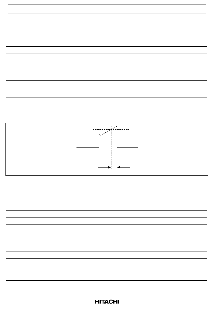
3. Current sensing response time tpd is definded a shown in the figure 1.
V
CS
V
OUT
(PWM)
Vth
tpd
Figure 1 Definition of Current Sensing Response Time tpd
PWM Output Part
Item
Symbol
Min
Typ
Max
Unit
Test Condition
Note
Output low voltage 1
V
OL1
--
0.7
1.5
V
losink = 20 mA
Output low voltage 2
V
OL2
--
1.5
2.2
V
losink = 200 mA
1
Output high voltage 1
V
OH1
13.0
13.5
--
V
losource = ≠20 mA
Output high voltage 2
V
OH2
12.0
13.3
--
V
losource = ≠200 mA
1
Output low voltage at
standby mode
V
OL STB
--
0.8
1.1
V
V
IN
= 5 V,
losink = 1 mA
Rise time
t
r
--
80
150
ns
C
L
= 1000 pF
Fall time
t
f
--
70
130
ns
C
L
= 1000 pF
Maximum ON duty
Du max
94
96
100
%
Minimum ON duty
Du min
--
--
0
%
Notes: 1. Pulse application test

HA17384SPS/SRP, HA17384HPS/HRP, HA17385HPS/HRP
10
Electrical Characteristics (cont)
UVL Part
Item
Symbol
Min
Typ
Max
Unit
Test Condition
Note
Threshold voltage for
V
TH UVL
14.5
16.0
17.5
V
Turn-ON voltage
1
high V
IN
level
7.6
8.4
9.2
V
when V
IN
is rising
2
Threshold voltage for
V
TL UVL
9.0
10.0
11.0
V
Minimum operating
1
low V
IN
level
6.8
7.6
8.4
V
voltage after turn-ON
2
V
IN
UVL hysteresis voltage
V
HYS UVL
5.0
6.0
7.0
V
V
HYS UVL
= V
TH UVL
≠ V
TL UVL
1
0.6
0.8
1.0
V
2
Vref UVL threshold voltage
V
T Vref
4.3
4.7
Vref
V
Voltage is forced toVref
terminal
Notes: 1. For the HA17384S/H.
2. For the HA17385H.
Total Characteristics
Item
Symbol
Min
Typ
Max
Unit
Test Condition
Note
Operating current
I
IN
7.0
10.0
13.0
mA
C
L
= 1000 pF, V
FB
= V
CS
= 0 V
Standby current
I
STBY
120
170
230
µ
A
Current at start up
Current of latch
I
LATCH
200
270
340
µ
A
V
FB
= 0 V after V
FB
= V
OVP
1, 2
Power supply zener
voltage
V
INZ
31
34
37
V
I
IN
+ 2.5 mA
Overheat protection
starting temperature
Tj
TSD
--
160
--
∞
C
3, 4
Notes: 1. These values are not prescribe to the HA17384SPS/SRP because OVP function is not included.
2. V
IN
= 8.5 V in case of the HA17384H.
2. These values are not prescribe to the HA17384SPS/SRP because TSD function is not included.
4. Reference value for design.
HA17384SPS/SRP, HA17384HPS/HRP, HA17385HPS/HRP
11
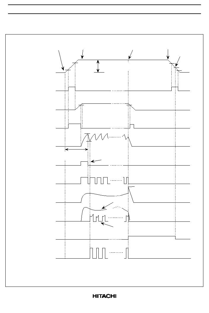
Timing Chart
Waveform timing (Outline)
Signal Name
Input voltage
V
IN
Pin 7
UVL1
Internal signal which
cannot be externally
monitored.
Reference voltage
Vref Pin 8
UVL2
Internal signal which
cannot be externally
monitored.
Oscillation voltage of
triangular wave
R
T
/C
T
Pin 4
Start up signal
Internal signal which
cannot be externally
monitored.
PWM latch setting signal
internal signal which
cannot be externally
monitored.
Error amplifier input signal
V
FB
Pin 2
Error amplifier output signal
V
COMP
Pin 1
I
D
*1
OVP latch signal
Internal signal which
cannot be externally
monitored.
Power ON
IC turn ON
Stationary operation
OVP input
OVP latched
condition
Power OFF
Reset of
OVP latch
Start up latch
release
( ) shows the case
using HA17385H
PWM output voltage
V
OUT
Pin 6
Note: 1. I
D
indicates the power MOSFET drain current; it is actually observed as voltage V
S
generated
by power MOSFET current detection source resistance R
S
.
V
COMP
indicates the error amp output voltage waveform. Current mode operation is
performed so that a voltage 1/3 that of V
COMP
is the current limiter level.
10 V
(7.6 V)
7.0 V
2 V
16 V
(8.4 V)
2 V
0V
0V
0V
0V
0V
0V
0V
0V
0V
0V
0V
5 V
4.7 V
2.8 V
1.2 V
7.0 V typ
(OVP input)
V
COMP
I
D
V
IN
4.7 V
IC operates and
PWM output stops.
This voltage is determined
by the transformer

HA17384SPS/SRP, HA17384HPS/HRP, HA17385HPS/HRP
12
Operation (Description of Timing Chart)
From Power ON to Turn On
After the power is switched ON, the power supply terminal voltage (V
IN
) of this IC rises by charging
through bleeder resistor R
B
. At this time, when the power voltage is in the range of 2 V to 16 V*
1
. The
low-voltage, lock out UVL1 operates and accordingly the OUT voltage, that is, the gate voltage of the
power MOSFET, is fixed at 1.3 V or a lower value, resulting in the power MOSFET remaining in the OFF
state.
When the power supply voltage reaches 16 V, UVL1 of this IC is reset and the reference voltage (Vref)
generating part turns ON. However, until Vref becomes 4.7 V, the low-voltage, lock out UVL2 operates to
keep the OUT terminal voltage low. After Vref terminal voltage becomes 4.7 V or higher, OUT terminal
outputs a PWM pulse.
Note: 1. The value is for the HA17384S/H.
The value is 8.4 V for the HA17385H.
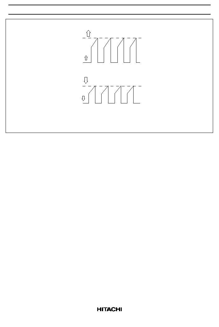
Generation of Triangular Wave and PWM Pulse
After the output of the Vref, each blocks begins to operate. The triangular wave is generated on the R
T
/C
T
terminal. For PWM pulses, the triangular wave rise time is taken as the variable on-duty on-time. The
triangular wave fall time is taken as the dead-band time. The initial rise of the triangular wave starts from 0
V, and to prevent a large on-duty at this time, the initial PWM pulse is masked and not output. PWM
pulses are outputted after the second triangular wave. The above operation is enabled by the charge energy
which is charged through the bleeder resistor R
B
into the capacitor C
B
of V
IN
.
Stationary Operation
PWM pulses are outputted after the second wave of the triangular wave and stationary operation as the
switching power supply starts.
By switching operation from ON/OFF to OFF/ON in the switching device (power MOSFET), the
transformer converts the voltage. The power supply of IC V
IN
is fed by the back-up winding of the
transformer.
In the current mode of the IC, the current in the switcing device is always monitored by a source resistor
R
CS
. Then the current limiter level is varied according to the error voltage (COMP terminal voltage) for
PWM control. One third of the error voltage level, which is divided by resistors "2R" and "R" in the IC, is
used to sense the current (R = 25 k
).
Two diodes between the error output and the 2R-R circuit act only as a DC level shifter. Actually, these
diodes are connected between the 2R-R circuit and GND, and, the current sensing comparator and GND,
respectively. Therefore, these blocks operate 1.4 V higher than the GND level. Accordingly, the error of the
current sensing level caused by the switching noise on the GND voltage level is eliminated. The zener
diode of 1 V symbolically indicates that the maximum sensing voltage level of the CS terminal is 1 V.
HA17384SPS/SRP, HA17384HPS/HRP, HA17385HPS/HRP
13
Power OFF
At power OFF, the input voltage of the transformer gradually decreases and then V
IN
of IC also decreases
according to the input voltage. When V
IN
becomes lower than 10 V*
2
or Vref becomes lower than 4.7 V,
UVL1 (UVL2) operates again and the PWM pulse stops.
Note: 2. The value is for the HA17384S/H.
The value is 7.6 V for the HA17385H.
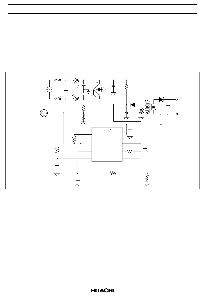
Commercial AC voltage
Power switch
Line filter
Rectifier
bridge diode
DC
output
Floating
ground
Power MOSFET
ex. 2SK1567
SBD
ex. HRP24
OVP input
(Ex: from photocoupler)
20k
3.6k
100
µ
200V
1000
µ
10V
R
T
10k
V
CS
R
B
220k
1/4W
C
B
10
µ
50V
V
IN
0.1
µ
51
1k
-
+
B
P
S
HRP32
Vref
V
IN
OUT
GND
COMP
FB
HA17384H,
HA17385H
CS
R
T
/C
T
+
-
+
-
+
-
+
-
R
CS
1
2W
100p
150k
330p
C
T
3300p
Figure 2 Mounting Circut Diagram for Operation Expression
HA17384SPS/SRP, HA17384HPS/HRP, HA17385HPS/HRP
14
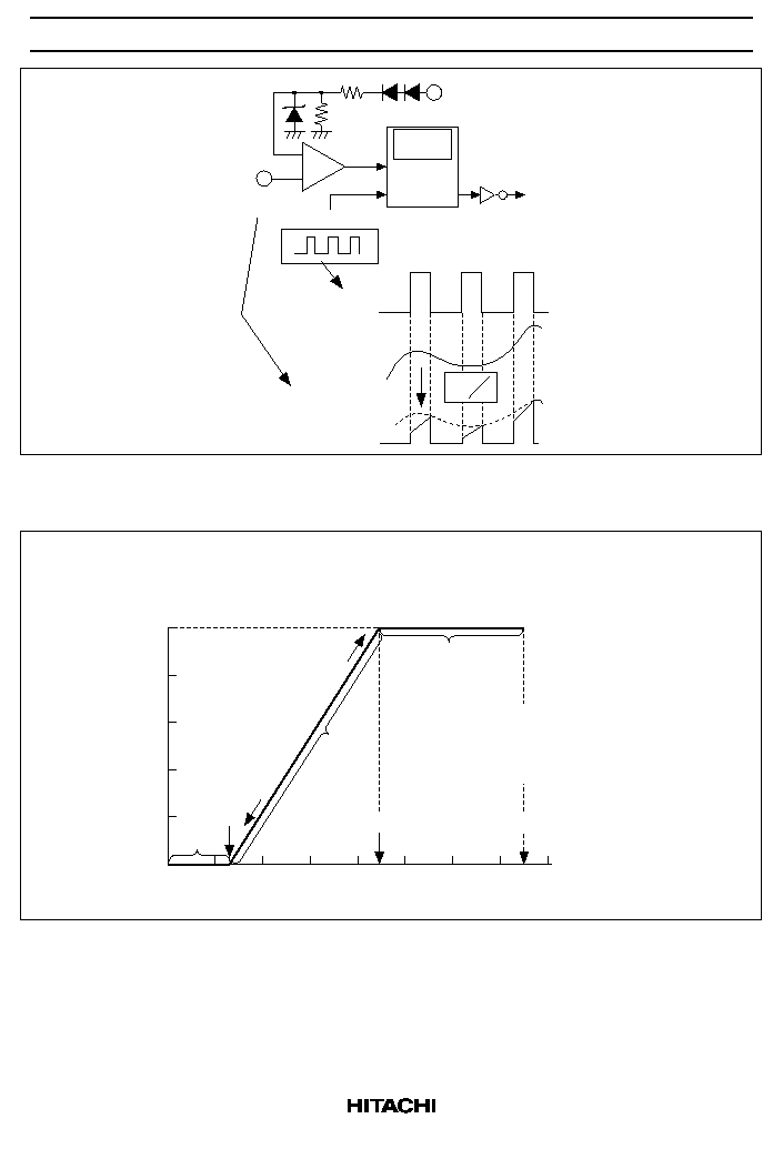
V
COMP
COMP terminal
(Error output)
PWM pulse
Latch setting pulse
(Implemented in triagular
wave oscillator)
Latch setting
pulse
V
COMP
Error voltage
V
CS
Current sensing
level
R
S
Q
1 V
V
CS
CS terminal
2 R
R
2V
F
◊
1
3
-
+
CS
CS
latch
Figure 3 Operation Diagram of Current Sensing Part
Point:
Current Sense Comparator
Threshold Voltage V
CS
(V)
Error Amplifier Output Voltage Vcomp (V)
Light load
Heavy load
1) At maximum rated load, the setting should be made to give
approximately 90% of area A below.
2) When the OVP latch is operated, the setting should be made
in area B or C.
1.0
0.8
0.6
0.4
0.2
0.0
0
1
2
3
4
5
6
7
8
B
A
C
1.4V
4.4V
7.5V
A : Stationary operation / PWM
(Current-mode operation)
B : Current limit operation / Max duty cycle
C : No sensitivity area / No PWM output
Figure 4 Current Sense Characteristics

HA17384SPS/SRP, HA17384HPS/HRP, HA17385HPS/HRP
15
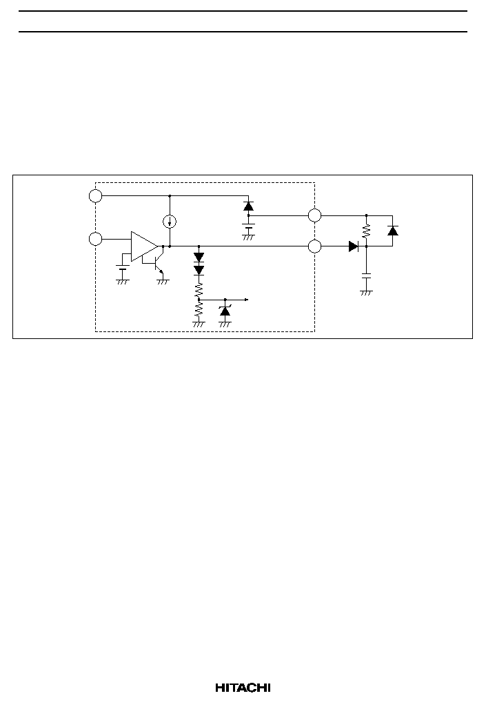
Features and Theory of Current Mode Control
Features of Current Mode Control
∑
Switch element current detection is performed every cycle, giving a high feedback response speed.
∑
Operation with a constant transformer winding current gives a highly stable output voltage (with
excellent line regulation characteristics, in particular).
∑
Suitable for flyback transformer use.
∑
External synchronous operation is easily achieved. (This feature, for example, is applicable to
synchronization with a forizontal synchronizing signal of CRT monitor.)
Theory of Current Mode Control
In current mode control, a PWM pulse is generated not by comparing an error voltage with a triangular
wave voltage in the voltage mode, but by changing the current limiter level in accordance with the error
voltage (COMP terminal in this IC, that is,output of the error amplifier output) which is obtained by
constantly monitoring the current of the switching device (power MOSFET) using source resistor R
CS
.
One of the features of current mode control is that the current limited operates in all cycles of PWM as
described by the above theory.
In voltage mode, only one feedback loop is made by an output voltage. In current mode, on the other hand,
two loops are used. One is an output voltage loop and the other is a loop of the switching device current
itself. The current of the switching device can be controlled switch high speed. In current mode control,
the current in the transformer winding is kept constant, resulting in high stability. An important
consequence is that the line regulation in terms of total characteristics is better than that in voltage mode.
Transformar
AC
input
Current sense
comparator
Error amplifier
DC
output
RS
2R
R
R
S
I
S
V
COMP
Vref
OSC
+
-
-
+
Flip flop
Figure 5 Block Diagram of Current Mode Switching Power Spply
HA17384SPS/SRP, HA17384HPS/HRP, HA17385HPS/HRP
16
A. Control in the case of heavy load
B. Control in the case of light load
V
CS
I
S
V
CS
I
S
As the load becomes heavy and the DC output decreases, the current sensing
level is raised as shown in A. above in order to increase the current in the switching
device in each cycle. When the load decreases, inverse control is carried out as
shown in B. above.
Figure 6 Primary Current Control of Transformer in Current Mode (Conceptual Diagram)

HA17384SPS/SRP, HA17384HPS/HRP, HA17385HPS/HRP
17
Main Characteristics
Operating Current I
IN
(mA)
Operating Current I
IN
(mA)
Operating Current I
IN
(mA)
Power supply voltage V
IN
(V)
Ambient temperature Ta (
∞
C)
Operating Current vs. Ambient Temperature
Standby Current/Latch Current vs. Supply Voltage
Exploded diagram of the small current part from the above figure
(HA17384S/H)
Power supply voltage V
IN
(V)
Standby Current/Latch Current vs. Supply Voltage
Exploded diagram of the small current part from the above figure
(HA17385H)
Power supply voltage V
IN
(V)
Power supply voltage V
IN
(V)
Ambient temperature Ta (
∞
C)
20
15
10
5
0
0
10
20
30
40
2.0
1.5
1.0
0.5
0
12
11
10
9
8
Ta
=
25
∞
C
Ta = 25
∞
C
fosc = 52kHz
C
T
= 3300pF
R
T
= 10k
Ta = 25
∞
C
fosc = 52kHz
C
T
= 3300pF
R
T
= 10k
20
15
10
5
0
0
10
20
30
40
Ta = 25
∞
C
0
10
20
30
40
2.0
1.5
1.0
0.5
0
0
10
20
30
40
400
300
200
100
0
Supply Current vs. Supply Voltage (HA17384S/H)
Supply Current vs. Supply Voltage (HA17385H)
Operating Current I
IN
(mA)
Operating Current I
IN
(mA)
Standby
Latch Current (
µ
A)
Standby Current/Latch Current vs. Ambient Temperature
Latch current
(HA17384H)
Latch current
(HA17384H)
Latch current
Stanby current
-
20
105
80
60
40
20
0
-
20
105
80
60
40
20
0
V
IN
= 15V
fosc = 52kHz
C
T
= 3300pF
R
T
= 10k
Latch current
V
IN
= 15V (HA17384H)
V
IN
= 8.5V (HA17385H)
Latch current
HA17384SPS/SRP, HA17384HPS/HRP, HA17385HPS/HRP
18
Ambient temperature Ta (
∞
C)
Ambient temperature Ta (
∞
C)
Ambient temperature Ta (
∞
C)
Supply voltage V
IN
(V)
Output current of Vref terminal (mA)
R
T
/C
T
terminal voltage V
CT
(V)
UVL Threshold Voltage vs. Ambient Temperature
Line Regulation Characteristics of Reference Voltage
Load Regulation Characteristics of Reference Voltage
Reference Voltage vs. Ambient Temperature
C
T
Discharge Current vs. R
T
/C
T
Terminal Voltage
C
T
Discharge Current vs. Ambient Temperature
UVL voltage (V)
Reference voltage Vref (V)
Reference voltage Vref (V)
Reference voltage Vref (V)
C
T
discharge current I
CT
(mA)
20
5.2
5.1
5.0
4.9
4.8
6.0
5.5
5.0
4.5
4.0
0
20
40
80
60
100
Ta = 25
∞
C
V
IN
= 15V
C
T
= 3300pF
R
T
= 10k
9.5
9.0
8.5
8.0
7.5
0
1
2
3
15
10
5
0
5.2
5.1
5.0
4.9
4.8
Ta = 25
∞
C
V
IN
= 15V
4
9.5
9.0
8.5
8.0
7.5
C
T
discharge current Isink
CT
(mA)
0
10
20
30
V
TL
V
TH
-
20
85
60
40
20
0
-
20
105
60
80
40
20
0
-
20
105
60
80
40
20
0
HA17385H
V
TH
HA17384S/H
V
TL
C
T
= 3300pF
R
T
= 10k
C
T
= 3300pF
R
T
= 10k
V
IN
= 15V
V
IN
=15 V
Ta = 25
∞
C
V
IN
= 10V or more (HA17384S/H)
V
IN
= 7.6V or more (HA17385H)
Vref short
protection
operates
Measured when
R
T
/C
T
terminal voltage
is externally supplied
Minimum voltage of
triangular wave
Maximum voltage of
triangular wave
Measured when R
T
/C
T
terminal voltage of 2 V is
externally supplied
HA17384SPS/SRP, HA17384HPS/HRP, HA17385HPS/HRP
19
Oscillation frequency fosc (kHz)
Timing resistance R
T
(
)
500
200
100
50
20
10
5
500
1k
2k
5k
10k
20k
50k 100k 200k
Ta = 25°C
V
IN
= 15V
2200pF
4700pF
0.01
µ
F
0.022
µ
F
0.047
µ
F
1000pF
C
T
=
470pF
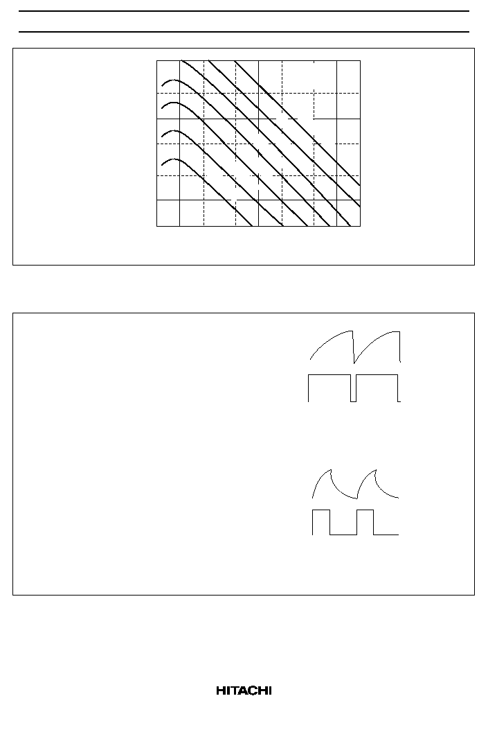
Figure 7 Oscillation Frequency vs. Timing Resistance
Triangular wave
PWM maximum ON pulse
In the case of small C
T
and large R
T
(ex. C
T
= 3300pF, R
T
= 10k
)
Du max = 95%
fosc = 52kHz
Triangular wave
PWM maximum ON pulse
In the case of large C
T
and small R
T
(ex. C
T
= 0.033
µ
F, R
T
= 680
)
Du max = 40%
fosc = 52kHz
Case 1.
Setting large maximum duty cycle.
Case 2.
Setting small maximum duty cycle.
Figure 8 Relationship Between Triangular Wave and Maximum ON Duty of PWM Pulse
HA17384SPS/SRP, HA17384HPS/HRP, HA17385HPS/HRP
20
Maximum ON duty Du max (%)
Timing Resistance R
T
(
)
Note: In the oscillation system of this IC, a constant discharging current of 8.4mA
flows the timing capacitor during triangular wave fall. Therefore, note that a
small maximum ON duty (large dead band) leads to a large supply current.
Refer to the equations of oscillation frequency and supply current for details.
100
75
50
25
0
500
1k
2k
5k
10k
20k
50k
100k 200k
Ta = 25
∞
C
V
IN
= 15V
Figure 9 PWM Pulse ON Duty vs. Timing Resistance

HA17384SPS/SRP, HA17384HPS/HRP, HA17385HPS/HRP
21
Oscillation Frequency fosc (kHz)
Ambient Temperature Ta (
∞
C)
Ambient temperature Ta (
∞
C)
Ambient temperature Ta (
∞
C)
Operating Current I
IN
(mA)
Maximum ON Duty Du max (%)
Output load capacitance C
L
(pF)
Oscillation Frequency vs. Ambient Temperature
Operating Current vs. Maximum ON Duty
Rise/Fall Time of Output Pulse vs. Load Capacitance
Rise/Fall Time of Output Pulse vs. Ambient Temperature
Rise/Fall Time (ns)
Rise/Fall Time (ns)
Current sensing level V
CS
(V)
V
IN
(UVL1)
Vref
(UVL2)
PWM
OUTPUT
Condition
description
L
L
L
L
H
L
H
H
L
Standby
state
IC is in
the ON
state and
output is
fixed to
LO.
Available
to
output
Current Sensing Level vs. Ambient Temperature
Relationship Between Low Voltage Malfunction
Protection and PWM Output
Operation
state
Standby
state
H
L
65
25
0
25
50
75
100
V
IN
= 15V
fosc=50kHz
fosc=300kHz
V
CS
= 0V
V
FB
= 0V
250
0
1000
2000
3000
Fall Time tf
60
55
50
45
40
20
15
10
5
0
200
150
100
50
0
V
IN
= 15V
V
CS
= 0V
V
FB
= 0V
Ta = 25
∞
C
C
T
= 3300pF
R
T
= 10k
4000
250
200
150
100
50
0
1.25
1.00
0.75
0.50
0.25
0
V
IN
= 15V
C
L
= 1000pF
C
T
= 3300pF
R
T
= 10k
Dumax = 95%
V
IN
= 15V
V
CS
= 0V
V
FB
= 0V
C
T
= 3300pF
R
T
= 10k
V
IN
= 15V
V
FB
= 0V
Rise time tr
C
L
= 1000pF
-
20
105
60
80
40
20
0
-
20
105
60
80
40
20
0
-
20
105
60
80
40
20
0
C
T
= 0.033
µ
F
R
T
= 680
Dumax = 40%
Ta=25
∞
C
C
L
= 1000pF
Rise time t
r
Fall Time t
f
Measured when COMP terminal
voltage is externally supplied

HA17384SPS/SRP, HA17384HPS/HRP, HA17385HPS/HRP
22
Gain A
VO
(dB)
Error Amplifier Input Signal Frequency f (Hz)
Gain A
VO
100
75
50
25
0
-
25
Phase
(deg)
0
60
120
180
10
100
1k
10k
100k
1M
10M
Phase
V
IN
= 15V, Ta = 25
∞
C
O
= 60
∞
Typ
Phase margin
at f
T
Unit gain frequency
f
T
= 1MHz Typ
Figure 10 Open Loop Gain Characterisrics of Error Amplifier
HA17384SPS/SRP, HA17384HPS/HRP, HA17385HPS/HRP
23
Triangular wave
PWM maximum
ON pulse
Dumax is the ratio of
maximum ON time of
PWM to one cycle time.
In the above case,
Dumax = 95%
∑
Calculation of operation parameters
1. Maximum ON duty Du max (Refer to the right figure.)
Du max =
1
1 + 1.78
◊
In 1 +
190
R
T
-
440
(
)
R
T
=
+ 440
190
0.56 (1/Du max
-
1)
C
T
= 1.78
◊
Du max
fosc
◊
R
T
ID
max
=
V
THCS
fosc =
1
C
T
◊
R
T
◊
0.56 + In 1 +
190
(
)
{
}
2. Oscillation frequency fosc
From the above two equations, the following two equations are
obtained.
3. Equalization to device R
T
from Du max
e
(e = 2.71828.base of natural logarithm)
4. Equation to device C
T
from fosc and R
T
5. Operating current I
IN
I
IN
= I
Q
+ Isink
CT
◊
(1
-
Du max) + Ciss
◊
V
IN
◊
fosc
providing that I
Q
= 8.4mA Typ (Supply current when oscillation in IC stops.)
Ciss is the input gate capacitance of the power MOSFET which is connected and V
IN
is
the supply voltage of the IC.
Note that the actual value may differ from the calculated one because of the internal
delay in operation and input characteristics of the POWER MOS FET. Check the
value when mounting.
Additionally a small Dumax leads to a large supply current, even if the frequency is
not changed, and start up may become difficult. In such a case, the following
measure is recommended.
Example 1: Calculation when R
T
= 10k
and C
T
= 3300pF
fosc = 52kHz, Du max = 95%, I
IN
= 9.7mA
Example 2: Calculation for 50% of Du max and 200 kHz of fosc
R
T
= 693
, C
T
= 6360pF, I
IN
= 12.5mA
(1) For an AC/DC converter, a small bleeder resistance is required.
(2) The large capacitance between Vref and GND is required.
(3) Use a large Dumax with a triangular wave and raise the current limit of the
switching device to around the maximum value (1.0V Typ).
The current limit is expressed as
R
T
-
440
However, Ciss = 1000pF, V
IN
= 18V
R
CS
-
1
Figure 11 Calculation of Operation Parameters
HA17384SPS/SRP, HA17384HPS/HRP, HA17385HPS/HRP
24
Application Circuit Example (1)
Notes:
P
Snubber circuit
example
51
470p
1kV
FRD
DFG1C8
1. : PRIMARY GND, : SECONDARY GND.
2. Check the wiring direction of the transformer coil.
3. Insert a snubber circuit if necessary.
4. OVP function is not included in HA17384SPS/SRP.
Commercial
AC 100V
Rectifier bridge diode
Line filter
Transformer specification
example
EI-22 type core
(H7C18
◊
06Z)
Gap length
lg = 0.3mm
Transformer coil example
P: 0.5ø80T/570
µ
H
S: 0.5ø16T Bifiler/22
µ
H
B: 0.2ø44T/170
µ
H
S
(Opetation Theory)
Because this circuit is a flyback type, the voltages in the
primary (P), secondary (s) coils of the transformer and
backup (B) coil are proportional to each other. Using this,
the output voltage of the backup coil (V
IN
of IC) is controlled
at constant 16.4V. (The voltage of the point divided by
resistors of 20k
and 3.6k
is 2.5V).
20k
3.6k
100
µ
200V
1000
µ
10V
R
T
10k
220k
1/4W
10
µ
50V
V
IN
16.4V
0.1
µ
51
1k
1k
-
+
B
P
S
HRP32
DC 5V, 3A
OUTPUT
Vref
V
IN
OUT
GND
COMP
FB
HA17384H,
HA17385H
2SK1567
SBD
HRP24
CS
R
T
/C
T
+
-
+
-
+
-
+
-
1
2W
100p
150k
470p
C
T
3300p
141V
10k
2SA1029
HA17431
10k
47k
Figure 12 Primary Voltage Sensing Flyback Converter
HA17384SPS/SRP, HA17384HPS/HRP, HA17385HPS/HRP
25
Application Circuit Example (2)
Photocoupler
(for output control)
Commercial
AC 100V
Rectifier bridge diode
When the error amplifier is used
Line filter
Transformer specification
example
EI-22 type core
(H7C18
◊
06Z)
Gap length
lg = 0.3mm
Transformer coil example
P: 0.5ø80T/570
µ
H
S: 0.5ø16T Bifiler/22
µ
H
B: 0.2ø44T/170
µ
H
(Operation Theory)
On the secondary side (S) of the flyback converter,
error amplification is carried out by a shunt
regulator and photocoupler.
The voltage of the backup coil (B) is not monitored,
which differs from the application example (1).
In addition, OVP operates on the secondary side
(S) using a photocoupler.
Refer to the application example (1) for the other
notes.
When the error
amplifier is not used
Bleeder resistor
(adjuster according
to the rating of the
Photocoupler)
100
µ
200V
1000
µ
10V
R
T
10k
220k
1/4W
10
µ
50V
V
IN
16.4V
141V
0.1
µ
51
1k
4.7k
-
+
B
P
S
HRP32
DC
5V, 3A
OUTPUT
Vref
V
IN
OUT
GND
COMP
FB
HA17384H,
HA17385H
HA17431
2SK1567
SBD
HRP24
CS
R
T
/C
T
R
T
/C
T
+
-
+
-
+
-
+
-
1.8k
B
4.7k
1
2W
100p
150k
470p
C
T
3300p
330
3.3
µ
3.3k
+
-
Vref
V
IN
OUT
GND
FB
CS
0.8mA
COMP
OVP input
1k
47k
HA17431
2SA1029
10k
10k
Figure 13 Secondary Voltage Sensing Flyback Converter
HA17384SPS/SRP, HA17384HPS/HRP, HA17385HPS/HRP
26
Application Examples for Fuller Exploitation of Power Supply Functions
A number of application examples are briefly described below.
1. Soft start
A soft start is a start method in which the PWM pulse width is gradually increased when the power
supply is activated. This prevents the stress on the transformer and switch element caused by a rapid
increase in the PWM pulse width, and also prevents overshoot when the secondary-side output voltage
rises. The circuit diagram is shown in figure 14.
-
+
EA
I
O
800
µ
A typ
Vref
5V
(3V)
(4.4V)
(3.7V)
(5V)
7
V
IN
D
IN
V
REF
R
CU
C
ST
D2
D1
2
2.5V
IC internal circuit
(around error amp.)
External circuit
(only partially shown)
FB
R
1V
To power supply
detection
comparator
(1V)
COMP
8
1
2R
Figure 14 Circuit Diagram for Soft Start
Operation: In this circuit, error amp output source current I
O
(800
µ
A typ.) gradually raises the switch
element current detection level, using a voltage slope that charges soft start capacitance C
ST
. When the
voltage at each node is at the value shown in parentheses in the figure, the soft start ends. The soft start
time is thus given by the following formula:
T
ST
= (3.7 V/800
µ
A)
◊
C
ST
4.62 C
ST
(ms)
(C
ST
unit:
µ
F)
External parts other than C
ST
operate as follows:
∑
Diode D1
: Current detection level shift and current reverse-flow prevention.
∑
Diode D2
: Together with diode D
IN
in the IC, C
ST
charge drawing when power supply falls.
∑
Resistance R
CU
: For C
ST
charge-up at end of soft start. (Use a high resistance of the order of several
hundred k
.)
Note:
During a soft start, since PWM pulses are not output for a while after the IC starts operating, there
is a lack of energy during this time, and intermittent mode may be entered. In this case, the
capacitance between Vref and GND should be increased to around 4.7
µ
F to 10
µ
F.
HA17384SPS/SRP, HA17384HPS/HRP, HA17385HPS/HRP
27
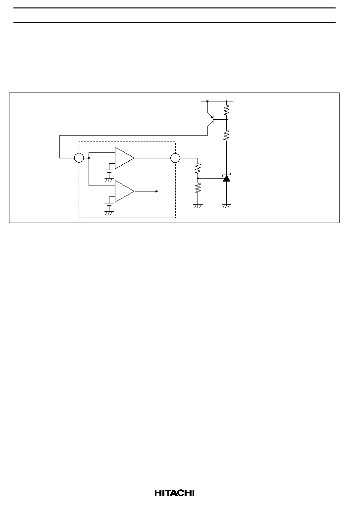
2. OVP latch output overvoltage protection (the HA17384H and HA17385H only)
The OVP latch is incorporated in the error amp input pin (FB). If the FB pin is pulled up to 7.0 V typ.
just once when the power supply enters any kind of error state, IC operation can be halted and held as it
is (latched). To reset the latch, drop the IC's supply voltage to 7.0 V typ. or below momentarily.
An OVP latch application example is shown in figure 15.
-
+
EA
V
IN
R
2
47k
2
2.5V
Inside IC
OVP comparator
FB
Error amplifier
-
+
OVP
7.0V
COMP
1
R
1
10k
HA17431
(Vref
2.5V)
1k
2SA1029
R
3
10k
External circuit
(only partially shown)
Figure 15 Example of OVP Latch Application Circuit
This circuit protects the system by causing latch operation in the event of an overload or load short. In
the steady state, the error amp input/output pins operate at 2.5 V typ., but if the load becomes heavy the
FB pin level drops and the COMP pin level rises. As shown in the figure, this is detected by the
HA17431 shunt regulator, and the FB pin level is pulled up, operating the OVP latch.
The operation parameters are as follows:
COMP pin voltage detection level: Vth = (R
1
+ R
2
) / R
2
◊
2.5 V
HA17384SPS/SRP, HA17384HPS/HRP, HA17385HPS/HRP
28
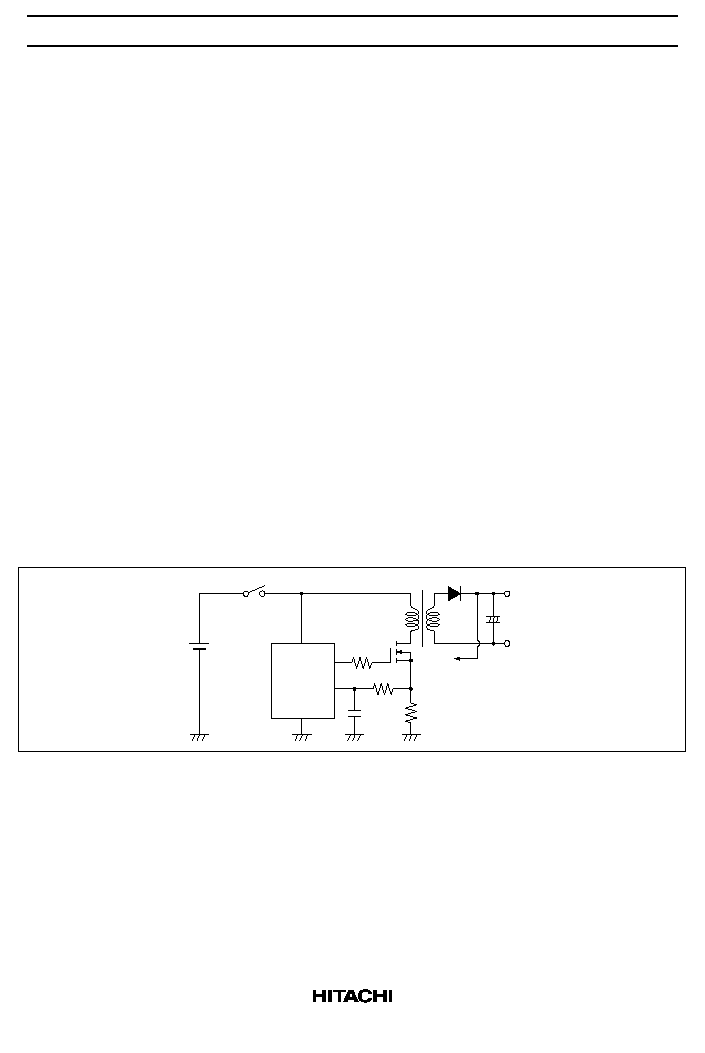
Notice for Use
1. OVP Latch Block
∑
Case
When DC power is applied directly as the power supply of the HA17384H, HA17385H, without using
the transformer backup coil. Also, when high-frequency noise is superimposed on the V
IN
pin.
∑
Problem
The IC may not be turn on in the case of a circuit in which V
IN
rises quickly (10 V/100
µ
s or faster),
such as that shown in figure 16. Also, the OVP latch may operate even though the FB pin is normally at
V
OVP
or below after the IC is activated.
∑
Reason
Because of the IC circuit configuration, the timer latch block operates first.
∑
Remedy (counter measure)
Take remedial action such as configuring a time constant circuit (R
B
, C
B
) as shown in figure 17, to keep
the V
IN
rise speed below 10 V/100
µ
s. Also, if there is marked high-frequency noise on the V
IN
pin, a
noise cancellation capacitor (C
N
) with the best possible high-frequency characteristics (such as a
ceramic capacitor) should be inserted between the V
IN
pin and GND, and close to the V
IN
pin.
When configuring an IC power supply with an activation resistance and backup winding, such as an
AC/DC converter, the rise of V
IN
will normally be around 1 V/100
µ
s, and there is no risk of this problem
occurring, but careful attention must be paid to high-frequency noise.
Also, this phenomenon is not occuring to the HA17384S, because OVP function is not built-in.
Output
Input
V
IN
V
IN
GND
Feedback
HA17384
Series
Figure 16 Example of Circuit with Fast V
IN
Rise Time

HA17384SPS/SRP, HA17384HPS/HRP, HA17385HPS/HRP
29
Output
Input
Time constant
circuit
Feedback
HA17384
Series
V
IN
V
IN
18V
R
B
51
C
N
C
B
1
µ
F
GND
+
Figure 17 Sample Remedial Circuit
2. Externally Synchronized Operation
∑
Case
When, with a power supply using the HA17384S/H or HA17385H, externally synchronized operation is
performed by applying an external syncronous signal to the R
T
/C
T
pin (pin 4).
∑
Problem
Synchronized operation may not be possible if the amplitude of the external syncronous signal is too
large.
∑
Reason
The R
T
/C
T
pin falls to a potential lower than the ground.
∑
Remedy (counter measure)
In this case, clamping is necessary using a diode with as small a V
F
value as possible, such as a schottky
barrier diode, as shown in figure 18.
Vref
0.01
µ
F
R
T
C
T
47
HA17384
Series
External
synchronous
signal
Figure 18 Sample Remedial Circuit
HA17384SPS/SRP, HA17384HPS/HRP, HA17385HPS/HRP
30
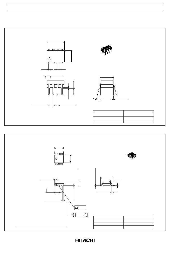
Package Dimensions
Hitachi Code
JEDEC
EIAJ
Mass (reference value)
DP-8
Conforms
Conforms
0.54 g
Unit: mm
1
4
5
8
9.6
10.6 Max
0.89
1.3
6.3
7.4 Max
2.54 Min
5.06 Max
2.54
±
0.25
0.48
±
0.10
7.62
0.25
+ 0.10
≠ 0.05
0
∞
≠ 15
∞
0.1 Min
1.27 Max
Hitachi Code
JEDEC
EIAJ
Mass (reference value)
FP-8DC
Conforms
--
0.085 g
Unit: mm
*Dimension including the plating thickness
Base material dimension
1.75 Max
4.90
0.25
0.15
0
∞
≠ 8
∞
M
8
5
1
4
1.27
3.95
0.40
±
0.06
*0.42
±
0.08
5.3 Max
0.75 Max
0.14
+ 0.11 ≠ 0.04
0.20
±
0.03
*0.22
±
0.03
0.60
+ 0.67
≠ 0.20
6.10
+ 0.10
≠ 0.30
1.08

HA17384SPS/SRP, HA17384HPS/HRP, HA17385HPS/HRP
31
Cautions
1. Hitachi neither warrants nor grants licenses of any rights of Hitachi's or any third party's patent,
copyright, trademark, or other intellectual property rights for information contained in this document.
Hitachi bears no responsibility for problems that may arise with third party's rights, including
intellectual property rights, in connection with use of the information contained in this document.
2. Products and product specifications may be subject to change without notice. Confirm that you have
received the latest product standards or specifications before final design, purchase or use.
3. Hitachi makes every attempt to ensure that its products are of high quality and reliability. However,
contact Hitachi's sales office before using the product in an application that demands especially high
quality and reliability or where its failure or malfunction may directly threaten human life or cause risk
of bodily injury, such as aerospace, aeronautics, nuclear power, combustion control, transportation,
traffic, safety equipment or medical equipment for life support.
4. Design your application so that the product is used within the ranges guaranteed by Hitachi particularly
for maximum rating, operating supply voltage range, heat radiation characteristics, installation
conditions and other characteristics. Hitachi bears no responsibility for failure or damage when used
beyond the guaranteed ranges. Even within the guaranteed ranges, consider normally foreseeable
failure rates or failure modes in semiconductor devices and employ systemic measures such as fail-
safes, so that the equipment incorporating Hitachi product does not cause bodily injury, fire or other
consequential damage due to operation of the Hitachi product.
5. This product is not designed to be radiation resistant.
6. No one is permitted to reproduce or duplicate, in any form, the whole or part of this document without
written approval from Hitachi.
7. Contact Hitachi's sales office for any questions regarding this document or Hitachi semiconductor
products.
Hitachi, Ltd.
Semiconductor & Integrated Circuits.
Nippon Bldg., 2-6-2, Ohte-machi, Chiyoda-ku, Tokyo 100-0004, Japan
Tel: Tokyo (03) 3270-2111 Fax: (03) 3270-5109
Copyright ' Hitachi, Ltd., 1998. All rights reserved. Printed in Japan.
Hitachi Asia Pte. Ltd.
16 Collyer Quay #20-00
Hitachi Tower
Singapore 049318
Tel: 535-2100
Fax: 535-1533
URL
NorthAmerica
: http:semiconductor.hitachi.com/
Europe
: http://www.hitachi-eu.com/hel/ecg
Asia (Singapore)
: http://www.has.hitachi.com.sg/grp3/sicd/index.htm
Asia (Taiwan)
: http://www.hitachi.com.tw/E/Product/SICD_Frame.htm
Asia (HongKong)
: http://www.hitachi.com.hk/eng/bo/grp3/index.htm
Japan
: http://www.hitachi.co.jp/Sicd/indx.htm
Hitachi Asia Ltd.
Taipei Branch Office
3F, Hung Kuo Building. No.167,
Tun-Hwa North Road, Taipei (105)
Tel: <886> (2) 2718-3666
Fax: <886> (2) 2718-8180
Hitachi Asia (Hong Kong) Ltd.
Group III (Electronic Components)
7/F., North Tower, World Finance Centre,
Harbour City, Canton Road, Tsim Sha Tsui,
Kowloon, Hong Kong
Tel: <852> (2) 735 9218
Fax: <852> (2) 730 0281
Telex: 40815 HITEC HX
Hitachi Europe Ltd.
Electronic Components Group.
Whitebrook Park
Lower Cookham Road
Maidenhead
Berkshire SL6 8YA, United Kingdom
Tel: <44> (1628) 585000
Fax: <44> (1628) 778322
Hitachi Europe GmbH
Electronic components Group
Dornacher Stra
e 3
D-85622 Feldkirchen, Munich
Germany
Tel: <49> (89) 9 9180-0
Fax: <49> (89) 9 29 30 00
Hitachi Semiconductor
(America) Inc.
179 East Tasman Drive,
San Jose,CA 95134
Tel: <1> (408) 433-1990
Fax: <1>(408) 433-0223
For further information write to: