
HA17451AP/HA17451AFP
Switching Regulator Controllers for DC/DC Converters
Description
The HA17451 is a dual-channel switching regulator controller IC. Each channel contains the basic circuits
for controlling a PWM-type switching-regulator power supply. Both channels are integrated onto the same
chip. Both channels can be completely synchronized, using the same oscillator output waveform. Each
channel can provide output voltages for step-up, step-down, inverting, and other converter topologies.
These controllers operate at voltages from 3.3 V to 40 V, making them suitable for a wide range of
applications. They are ideal for chopper-type DC/DC converters. They are similar to the TL1451, but note
that the HA17451A differs from the TL1451A.
Functions
∑
Low-dropout 2.5V voltage reference
∑
Undervoltage lockout
∑
Triangle-wave oscillator
∑
Adjustable dead-time control
∑
Error amplifier
∑
Output driver (open-collector transistor type)
∑
PWM comparator

HA17451AP/HA17451AFP
2
Features
∑
Low dropout voltage of on-chip 2.5V voltage reference: Vdrop = 0.2 V (typ)
∑
Operates throughout wide supply voltagerange: 3.3 V to 40 V
∑
Large maximum output current: 50 mA (max)
∑
Undervoltage lockout circuit
High threshold voltage: 3.15 V (typ)
Low threshold voltage: 2.98 V (typ)
∑
Low current drain: 1.5 mA (typ)
∑
Operates at wide range of oscillator frequencies: f
OSC
= 1 kHz to 300 kHz
∑
Dead time adjustable through full duty cycle range
∑
Surface-mount package (SOP16) for saving space (HA17451AFP)
Ordering Information
Type Name
Package
HA17451AP
DP-16
HA17451AFP
FP-16DA
HA17451AP/HA17451AFP
3
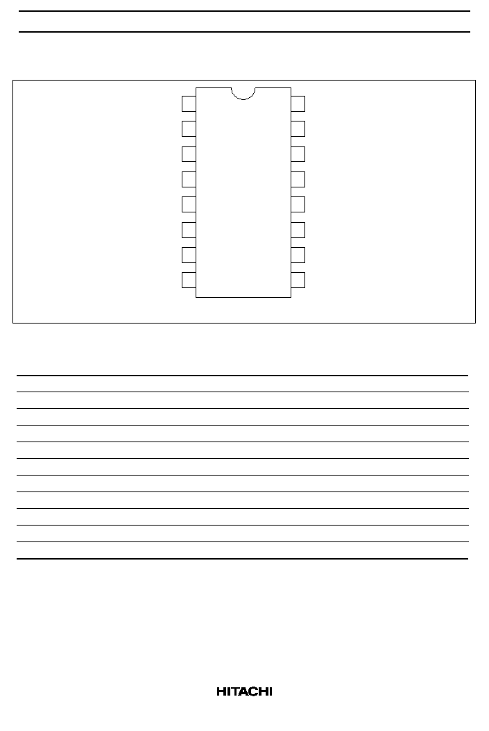
Pin Arrangement
1
2
3
4
5
6
7
8
9
10
11
12
13
14
15
16
C
T
R
T
NON. INV.
INPUT1
INV.
INPUT1
FEED
BACK1
D.T.C1
OUT1
GND
Vref
NON. INV.
INPUT2
INV.
INPUT2
FEED
BACK2
D.T.C2
OUT2
V
CC
S.C.P
(Top view)
Pin Functions
Pin No.
Symbols
Functions
1
C
T
Timing capacitor
2
R
T
Timing resistor
3, 14
NON. INV. INPUT
Non-inverting input of error amp
4, 13
INV. INPUT
Inverting input of error amp
5, 12
FEEDBACK
Output of error amp
6, 11
D.T.C
Dead time control
7, 10
OUT
Output
8
GND
Ground
9
V
CC
Input voltage
15
S.C.P
Short circuit protection
16
Vref
Reference voltage output
HA17451AP/HA17451AFP
4
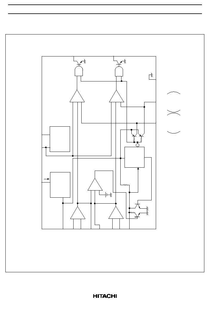
Block Diagram
V
CC
Reference
voltage
generation
circuit
Triangle
oscillator
OUT1
Output1
OUT2
Output2
DEAD
TIME
CONTROL2
DEAD
TIME
CONTROL1
GND
R
Under-
voltage
lockout
Vref /2
Error amp2
Short circuit
protection
comparator
PWM
comparator2
PWM
comparator1
+
≠
+
≠
+
≠
+
Vref
NON. INV. INPUT1
INV. INPUT1
FEEDBACK1
FEEDBACK2
NON. INV. INPUT2
INV. INPUT2
S.C.P
(16)
(3)
(4)
C
R
TT
(6)
Vref
(5)
(12)
(14)
(15)
(11)
(8)
D.T.C2
D.T.C1
(10)
(7)
(2)
(1)
(9)
Error amp1
+ ≠ ≠
+ ≠ ≠
(13)
HA17451AP/HA17451AFP
5
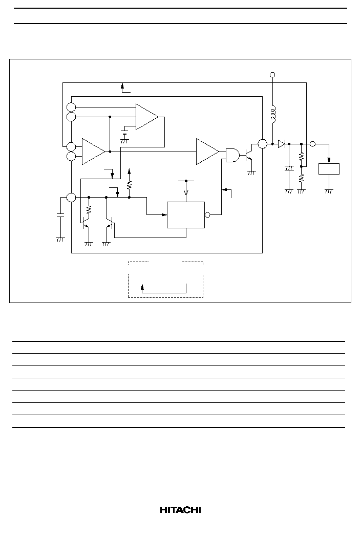
Short-circuit Protection in HA17451A
5
12
15
(2)
14
13
10
(1)
(3)
+
+
≠
+
≠
≠
+
≠
High
Low
Error Amp2
Low
1.23 V
Vref
Vref
PWM Comparator2
Feedback line
Load
(voltage drop)
V
B
Vout
R
U.V.L.O.
Also used as positive feedback route
Positive
feedback
Shutdown
(1)Overcurrent
(2)Vout drops
(3)Output turns off
Absolute Maximum Ratings (Ta = 25
∞
C)
Item
Symbol
Rating
Unit
Note
Power supply voltage
V
CC
40
V
Error amplifier input voltage
V
I
20
V
Collector output voltage
V
O
40
V
Collector output current
I
O
50
mA
Power dissipation
P
T
680
mW
*
Operating temperature
Topr
-
20 to +85
∞
C
Storage temperature
Tstg
-
55 to +125
∞
C
Note:
This value applies to the HA17451AP at ambient temperatures up to Ta = 45
∞
C. Derate by8.3
mW/
∞
C above that point.