 | –≠–ª–µ–∫—Ç—Ä–æ–Ω–Ω—ã–π –∫–æ–º–ø–æ–Ω–µ–Ω—Ç: HA17524FP | –°–∫–∞—á–∞—Ç—å:  PDF PDF  ZIP ZIP |

HA17524P/FP
Switching Regulator Controller
Features
∑
Pulse width modulation (PWM)
∑
Wide oscillation frequency range: 450 kHz(typ)
∑
Low quiescent current: 5 mA typ
∑
Good line regulation (0.2% typ) and load regulation (0.4% typ)
∑
Independent output stages for 2 channels
∑
Wide external circuit applications including single-end and push-pull method
∑
Reference power source output stage and switching output stage include current limiting protection
circuit.
Ordering Information
Type No.
Package
HA17524P
16 pin dual in line plastic(DP-16)
HA17524FP
16 pin flat plastic (FP-16DA)
Pin Arrangement
1
2
3
4
5
6
7
8
16
15
14
13
12
11
10
9
NON-INV.
Input
OSC Out
CL(+)
CL(≠)
GND
R
T
C
T
INV.
Input
SHUT
DOWN
COMP
V
REF
V
CC
E
C
2
2
C
1
E
1
(Top View)
HA17524P/FP
2
Functional Description
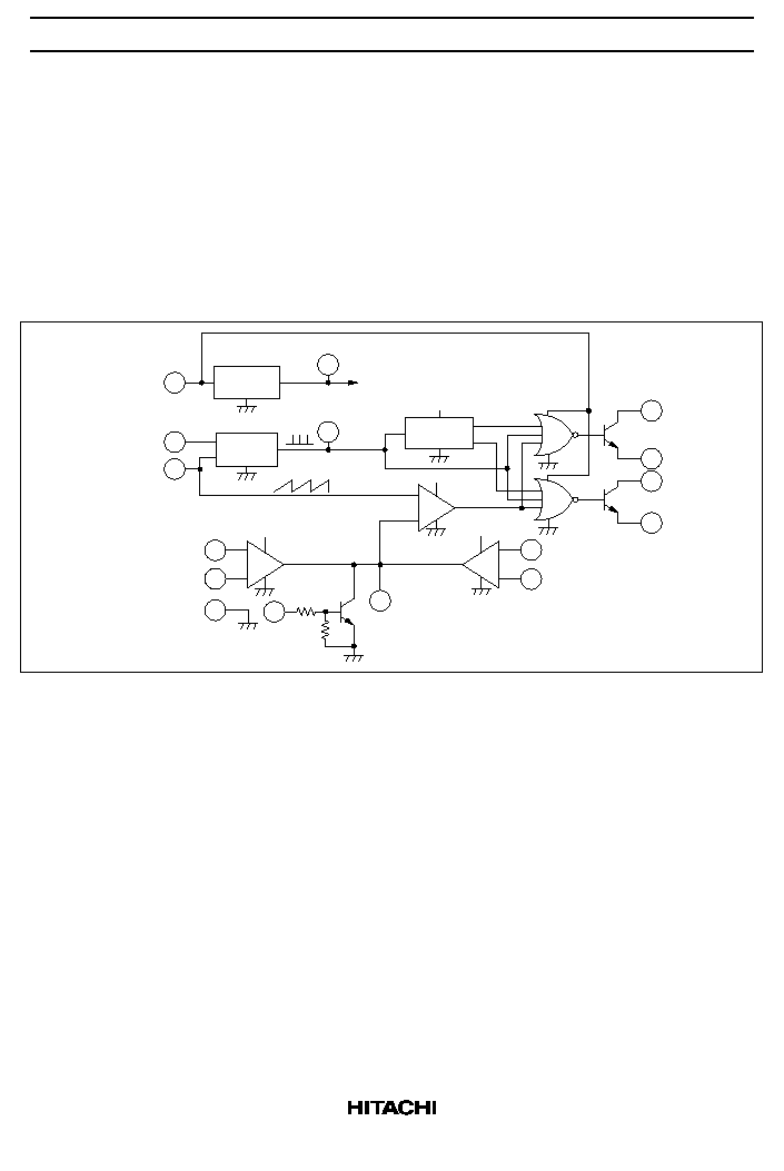
Principals of HA17524 Operation
The HA17524 switching regulator circuit, using pulse width modulation (PWM), is constructed as shown
in figure 1.
Timing resistances R
T
and timing capacitance C
T
control the oscillation frequency. C
T
is charged by a
constant current generated by R
T
. Ramp signals (saw-tooth waves) at the C
T
terminal generated by this
oscillator is available for reference input signal to comparator which control the pulse width.
Ref.
Volt.
+5 V
V
REF
+5V
INV. Input
NON-INV. Input
--
+
+
--
C.L.
--
+
+5V
V
CC
COMP
GND
SHUT
DOWN
Error Amp.
Current Limiter
+5V
CL(+)
CL(--)
NOR
NOR
C
1
Q
1
Q
2
E
1
C
2
E
2
+5V
Q
Q
+5 V to internal circuitry
OSC Out
Comparator
R
T
C
T
(Ramp)
1k
10k
Flip Flop
Osc.
16
3
6
7
1
2
8
10
9
5
4
14
13
11
12
15
Figure 1 HA17524 Block Diagram
The reference voltage connects to the non-inverted or inverted input terminal of the error amplifier via
resistance divider (figure 2).
The output voltage from the error amplifier is compared with the ramp signal capacitance C
T
(figure 1).
The comparator can provide a signal with modulated pulse width.
This signal, then, controls output transistors Q
1
and Q
2
, making an open loop to stabilize output voltage.
Outputs form the error amplifier the current limiter, and the shut-down circuit are connected together at the
comparator, so that an input signal from any one of these circuits can break the output stage.

HA17524P/FP
3
+
-
+
-
V
REF
5k
5k
5k
5k
R
2
R
1
To Positive Regulated
Output Voltage V
O
(a) Forward Output Stabilizing Source
V
REF
R
1
R
2
To Negative Regulated
Output Voltage V
O
(b) Reverse Output Stabilizing Source
V = 2.5 (V)
O
R + R
R
1
2
1
O
V = 5
-
2.5 (V)
R + R
R
2
1
1
Error Amp
Error Amp
Figure 2 Error Amplifier Biasing

HA17524P/FP
4
Blocks Description
Oscillator: The oscillation frequency f is calculated from the following equations. Figure 3 shows one
example.
f 1.15/(R
T
∑C
T
)
R
T
= 1.8k to 100 k
C
T
= 0.001
µ
to 0.1
µ
F
f = 140 Hz to 500 kHz
1 k
4 k
10 k
40 k 100 k
100
400
1 k
4 k
10 k
40 k
100 k
400 k
1 M
Timing Resistance R ( )
T
Oscillating Frequency f (Hz)
V = 20 V
Ta = 25
∞
C
CC
C = 0.1 F
T
µ
C = 0.01 F
T
µ
C = 0.001 F
T
µ
Figure 3 Oscillating Frequency vs Timing Resistance
Then the ramp wave shown in figure 4 is available at pin 7, C
T
terminal, since C
T
is charged by the constant
current I generated by R
T
.

HA17524P/FP
5
I
I
Q
1
R
T
C
T
Q
2
V
REF
Q
Discharge
3
V
H
V
L
V
T
C
T
Terminal Waveform
V = V ≠ V
L
3.8 ≠ 0.9 = 2.9 V
H
V
REF
≠ V
EB
(Q
2
) ≠ V
EB
(Q
3
)
T C
T
∑
V ∑
1
I
I
R
T
6
7
Figure 4 Oscillating Circuit and C
T
Terminal Waveform
The oscillator output pulse signal is used as the flip flop clock pulse and as switching pulses for the output
transistors, synchronous to the clock pulse.
The pulse-widths which can be controlled by the timing capacitor C
T
as shown in figure 5, increases output
dead time.
0.001
0.003
0.01
0.03
0.1
0.1
0.3
1.0
3
10
Timing Capacitance C
T
(
µ
F)
Dead
T
ime (
µ
s)
V = 20 V
R = 10 k
Ta = 25
∞
C
CC
T
Figure 5 Dead Time vs Timing Capacitance
Reference Voltage: The built-in regulator (reference voltage: V
REF
= 5 ±0.4 V) can be used as a reference
power supply for the error amplifier, which determines output voltage (V
OUT
). It is also connected as a bias
source for another circuits in IC.