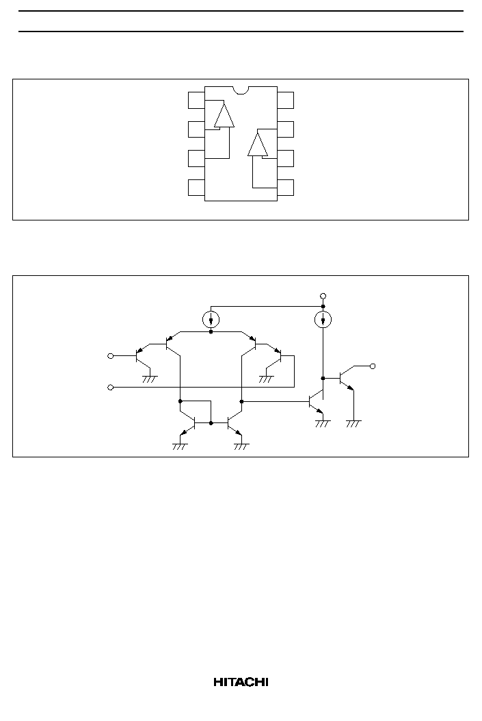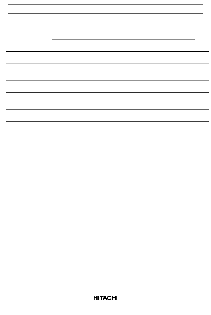
HA17903, HA17393 Series
Dual Comparator
Description
HA17903 and HA17393 are comparators designed for car use and control system use.
They provide wide voltage range with single power source, and the change of supply current is small,
because it is independent of the supply voltage. They can be widely applied, such as limit comparator,
simple analog/digital converter, pulse/square wave/time delay generator, wide range VCO, MOS clock
timer, multivibrator, high voltage logic gate, etc.
Features
∑
Wide supply voltage: 2 to 36V
∑
Very low supply current: 0.8mA
∑
Small input bias: 25nA
∑
Small input offset current: 3nA
∑
Small input offset voltage: 2mV
∑
Common mode input voltage range including ground.
∑
Small output saturation voltage: 1mV (5µA)
70mV (1mA)
∑
Output voltage is compatible with CMOS logic system.
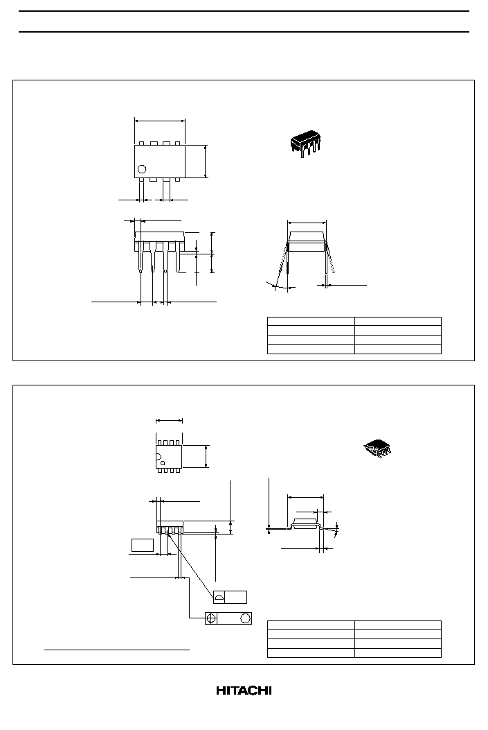
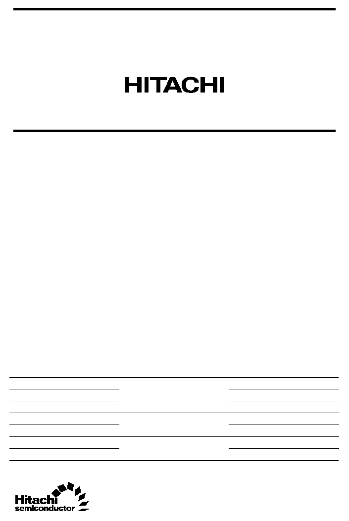
Ordering Information
Type No.
Application
Package
HA17903PSJ
Car use
DP-8
HA17903FPJ
FP-8D
HA17903FPK
FP-8D
HA17903PS
Industrial use
DP-8
HA17903FP
FP-8D
HA17393
Commercial use
DP-8
HA17393F
FP-8D
HA17903, HA17393 Series
4
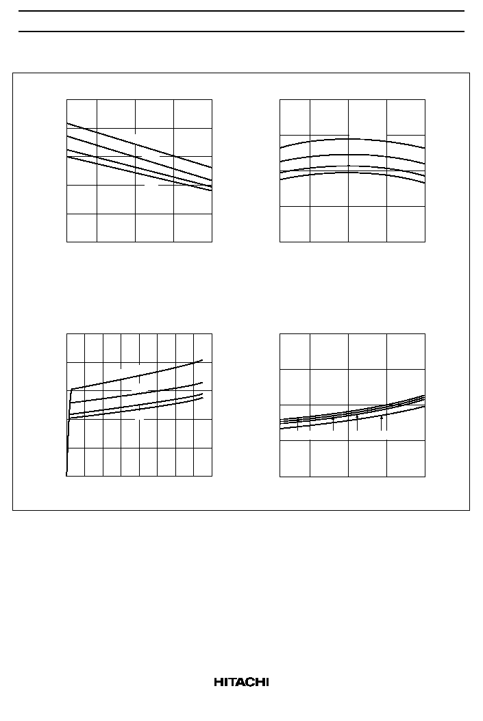
Electrical Characteristics-1 (V
CC
= 5V, Ta = 25∞C)
Item
Symbol
Min
Typ
Max
Unit
Test condition
Input offset voltage*
1
V
IO
--
2.0
5.0
mV
Input bias current*
2
I
IB
--
25
250
nA
I
IN (+)
or I
IN (≠)
Input offset current
I
IO
--
3
50
nA
|
I
IN (+)
≠ I
IN (≠)
|
Common mode input
voltage*
3
V
CM
+
3.5
--
--
V
V
CM
≠
--
--
0
V
Supply current
I
CC
--
0.8
2.0
mA
All comparators: R
L
=
,
All channels on
Voltage gain
A
VD
--
200
--
V/mV
V
CC
= 15V, R
L
15k
Response time*
4
t
R
--
1.3
--
µ
s
V
RL
= 5V, R
L
= 5.1k
Large signal response
time
t
RI
--
300
--
ns
V
IN
= TTL Threshold width, V
REF
= 1.4V
Out put sink current
Iosink
6
16
--
mA
V
IN (≠)
1V, V
IN (+)
= 0, V
O
1.5V
Output saturation voltage
V
O
(sat)
--
--
400
mA
V
IN (≠)
1V, V
IN (+)
= 0,
Iosink = 4mA
Output leak current
I
LO
--
0.1
--
nA
V
IN (≠)
= 0, V
IN (+)
1V, V
O
= 5V
Notes: 1. V
REF
= 1.4V and R
S
= 50
, when V
O
= 1.4V at output switching point.
2. Under linear operation.
3. Common mode input voltage or each one of the input signal should not be less than ≠0.3V.
4. This is a value to 100mV input step voltage with 5mV over drive.
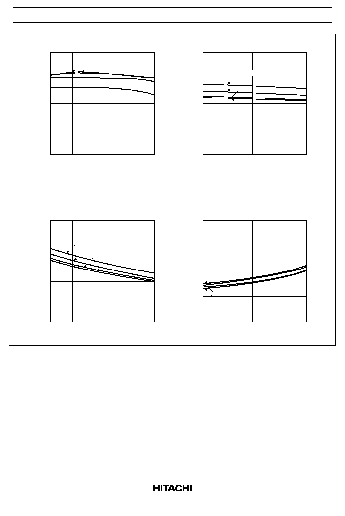
Electrical Characteristics-2 (V
CC
= 5V, Ta = ≠40 to +125∞C)
Item
Symbol
Min
Typ
Max
Unit
Test condition
Input offset voltage*
1
V
IO
--
--
5.0
mV
Input offset current
I
IO
--
--
200
nA
|
I
IN (+)
≠ I
IN (≠)
|
Input bias current
I
IB
--
--
500
nA
Output linear range
Common mode input
voltage
V
CM
0
--
V
CC
≠
2.0
V
Output saturation voltage
V
O
(sat)
--
--
440
mV
V
IN (≠)
1V, V
IN (+)
= 0,
Iosink
4mA
Output leak current
I
LO
--
1.0
--
µ
A
V
IN (≠)
= 0, V
IN (+)
1 V, V
O
= 30V
Supply current
I
CC
--
--
4.0
mA
All comparators: R
L
=
,
All channels on
Note:
1. V
REF
= 1.4V and R
S
= 50
, when V
O
= 1.4V at the output switching point.
HA17903, HA17393 Series
8
Cautions
1. Hitachi neither warrants nor grants licenses of any rights of Hitachi's or any third party's patent,
copyright, trademark, or other intellectual property rights for information contained in this document.
Hitachi bears no responsibility for problems that may arise with third party's rights, including
intellectual property rights, in connection with use of the information contained in this document.
2. Products and product specifications may be subject to change without notice. Confirm that you have
received the latest product standards or specifications before final design, purchase or use.
3. Hitachi makes every attempt to ensure that its products are of high quality and reliability. However,
contact Hitachi's sales office before using the product in an application that demands especially high
quality and reliability or where its failure or malfunction may directly threaten human life or cause risk
of bodily injury, such as aerospace, aeronautics, nuclear power, combustion control, transportation,
traffic, safety equipment or medical equipment for life support.
4. Design your application so that the product is used within the ranges guaranteed by Hitachi particularly
for maximum rating, operating supply voltage range, heat radiation characteristics, installation
conditions and other characteristics. Hitachi bears no responsibility for failure or damage when used
beyond the guaranteed ranges. Even within the guaranteed ranges, consider normally foreseeable
failure rates or failure modes in semiconductor devices and employ systemic measures such as fail-
safes, so that the equipment incorporating Hitachi product does not cause bodily injury, fire or other
consequential damage due to operation of the Hitachi product.
5. This product is not designed to be radiation resistant.
6. No one is permitted to reproduce or duplicate, in any form, the whole or part of this document without
written approval from Hitachi.
7. Contact Hitachi's sales office for any questions regarding this document or Hitachi semiconductor
products.
Hitachi, Ltd.
Semiconductor & Integrated Circuits.
Nippon Bldg., 2-6-2, Ohte-machi, Chiyoda-ku, Tokyo 100-0004, Japan
Tel: Tokyo (03) 3270-2111 Fax: (03) 3270-5109
Copyright ' Hitachi, Ltd., 1998. All rights reserved. Printed in Japan.
Hitachi Asia Pte. Ltd.
16 Collyer Quay #20-00
Hitachi Tower
Singapore 049318
Tel: 535-2100
Fax: 535-1533
URL
NorthAmerica
: http:semiconductor.hitachi.com/
Europe
: http://www.hitachi-eu.com/hel/ecg
Asia (Singapore)
: http://www.has.hitachi.com.sg/grp3/sicd/index.htm
Asia (Taiwan)
: http://www.hitachi.com.tw/E/Product/SICD_Frame.htm
Asia (HongKong)
: http://www.hitachi.com.hk/eng/bo/grp3/index.htm
Japan
: http://www.hitachi.co.jp/Sicd/indx.htm
Hitachi Asia Ltd.
Taipei Branch Office
3F, Hung Kuo Building. No.167,
Tun-Hwa North Road, Taipei (105)
Tel: <886> (2) 2718-3666
Fax: <886> (2) 2718-8180
Hitachi Asia (Hong Kong) Ltd.
Group III (Electronic Components)
7/F., North Tower, World Finance Centre,
Harbour City, Canton Road, Tsim Sha Tsui,
Kowloon, Hong Kong
Tel: <852> (2) 735 9218
Fax: <852> (2) 730 0281
Telex: 40815 HITEC HX
Hitachi Europe Ltd.
Electronic Components Group.
Whitebrook Park
Lower Cookham Road
Maidenhead
Berkshire SL6 8YA, United Kingdom
Tel: <44> (1628) 585000
Fax: <44> (1628) 778322
Hitachi Europe GmbH
Electronic components Group
Dornacher Stra
e 3
D-85622 Feldkirchen, Munich
Germany
Tel: <49> (89) 9 9180-0
Fax: <49> (89) 9 29 30 00
Hitachi Semiconductor
(America) Inc.
179 East Tasman Drive,
San Jose,CA 95134
Tel: <1> (408) 433-1990
Fax: <1>(408) 433-0223
For further information write to: