 | –≠–ª–µ–∫—Ç—Ä–æ–Ω–Ω—ã–π –∫–æ–º–ø–æ–Ω–µ–Ω—Ç: HA19216 | –°–∫–∞—á–∞—Ç—å:  PDF PDF  ZIP ZIP |

HA19216/MP
6-Bit Flash Type Analog-to Digital Converter
Description
The HA19216/MP bipolar LSI performs high speed 6-bit A/D conversion. Digital data output and clock
input terminals are compatible with TTL and CMOS. The HA19216/MP are designed for video signal
processing application.
Features
∑
6-bit resolution (including overflow)
∑
6-bit latched three-state outputs
∑
Maximum conversion Rate: 20 Msps (Min)
∑
Single Power Supply: +5 V
∑
Digital data output, high impedance state control and clock input terminals compatible with TTL and
CMOS
∑
Needs no sample and hold circuit
∑
18-pin DIP package and 28-pin surface mount package.
∑
Output current:
I
OL
= 1.4 mA (guaranteed)
I
OH
= ≠5 mA (guaranteed)
Application
∑
Pattern recognition using a computer
∑
High-speed measuring instruments
Ordering Information
Type No.
Package
HA19216
300mil 18 pin plastic DIP (DP-18A)
HA19216MP
28 pin plastic QFI (MP-28)

HA19216/MP
2
Pin Arrangement
B6
OF
GND
NC
CE2
CLK
PHASE
V
RT
CE1
V
RB
B5
B4
B3
B2
B1
V
CC
V
IN
V
RM
(Top View)
(Top View)
1
2
3
4
5
6
7
8
9
18
17
16
15
14
13
12
11
10
OF
NC
B6
B5
NC
B4
NC
PHASE
NC
V
IN
NC
GND
NC
CE2
NC
CE1
NC
CLK
NC
V
RM
B3
B2
B1
NC
NC
V
CC
3
2
1
28
27
26
12
13
14
15
16
17
4
5
6
7
8
9
10
11
25
24
23
22
21
20
19
18
V
RB
V
RT
∑ HA19216
∑ HA19216MP
Pin Function
Pin No.
HA19216
HA19216MP
Symbol
Function
Remarks
1
1
B6
Bit 6 digital output (MSB)
2
3
OF
Digital output (Overflow)
3
5
GND
Ground
4
--
NC
Not connected
5
7
CE2
Digital output high
Impedance control
input
6
9
CE1
Digital output high
Impedance control
input
7
11
CLK
Clock input
8
13
PHASE
Clock phase control input
9
14
V
RT
High level reference voltage input
10
15
V
BR
Low level reference voltage input
11
17
V
IN
Analog input
12
19
V
CC
Power supply
13
21
B1
Bit 1 digital output (LSB)

HA19216/MP
3
Pin Function (Cont)
Pin No.
HA19216
HA19216MP
Symbol
Function
Remarks
14
22
B2
Bit 2 digital output
15
23
B3
Bit 3 digital output
16
24
V
RM
Reference voltage center tap
17
26
B4
Bit 4 digital output
18
28
B5
Bit 5 digital output
Note:
CE1
CE2
B1 ≠ B6
OF
◊
L
Z
Z
L
H
H/L
H/L
H
H
Z
H/L
H: High level
L: Low level
◊
: Don't care
Z: High impedance

HA19216/MP
4
Block Diagram
CLK
7
8
11
9
R/2
PHASE
V
IN
V
RT
16
10
V
RM
V
RB
R
R
R
R
R
R
R/2
Comparators and Latches
Comp.
1
Comp.
2
Comp.
33
Comp.
63
Comp.
64
Encoder
Logic
High Impedance
State
Buffer
Q
D
CLK
Q
D
CLK
Q
D
CLK
Q
D
CLK
Q
D
CLK
Q
D
CLK
Q
D
CLK
3
GND
5
CE2
6
CE1
13 B1 (LSB)
14 B2
15 B3
17 B4
18 B5
1
B6 (MSB)
2
OF
12
V
CC
(19)
(13)
(17)
(14)
(24)
(15)
(5)
(7)
(9)
(22)
(21)
(23)
(26)
(28)
(1)
(3)
(11)
indicates HA19216 pin number
indicates HA19216MP pin number
r
( )

HA19216/MP
5
Interface
64 Comparators
11
V
CC
V
IN
Figure 1 Analog Input
V
CC
V
CLK
V
PHASE
7
8
100
Figure 2 Clock Input
V
CC
V
CE1
V
CE2
6
5
100
Figure 3 High Impedance State Control Input

HA19216/MP
6
2
V
CC
1
18
17
15
14
13
OF
B6
B5
B4
B3
B2
B1
High Impedance State
Control
Same as Pin 2
Figure 4 Digital Output
Absolute Maximum Ratings (Ta = 25
∞
C, unless otherwise specified)
Item
Symbol
Rating
Unit
Supply voltage
V
CC
+7.0
V
Input signal voltage*
V
IN
0 to V
CC
V
Input reference voltage*
V
R
0 to V
CC
V
Digital input voltage
V
I
0 to V
CC
V
Voltage applied to digital output pin in high
impedance
V
O
0 to V
CC
V
Power dissipation
P
T
550
mW
Operating temperature
Topr
0 to +70
∞
C
Storage temperature
Tstg
≠55 to +125
∞
C
Reference voltage difference
V
RT
≠ V
RB
1.3
V
Reference center tap voltage
V
RM
Open state voltage
±
0.1
V
Note:
V
IN
and V
R
should not be lower than 1.5 V at the same time.

HA19216/MP
7
Electrical Characteristics (Ta = 25
∞
C, V
CC
= 5.0 V, V
RT
= 3.0 V, V
RB
= 2.0 V, unless
otherwise specified)
Item
Symbol
Min
Typ
Max
Unit
Test Condition
Resolution
6
6
6
bits
Operating supply voltage
V
CC
4.75
5.0
5.25
V
Quiescent current
I
CC
--
50
84
mA
f
CLK
= 20 Msps
Digital input voltage
High
V
IH
2.0
--
V
CC
V
Low
V
IL
0
--
0.8
V
Digital input current
High
I
IH
--
--
100
µ
A
V
I
= 2.7 V
Low
I
IL
≠100
--
--
µ
A
V
I
= 0.4 V
Digital output voltage High
V
OH
3.4
3.8
--
V
I
OH
= ≠5 mA
Low
V
OL
--
0.61
0.76
V
I
OL
= 1.4 mA
Digital output current
High
I
OZH
--
--
100
µ
A
V
O
= 5.0 V
(High impedance)
Low
I
OZL
≠100
--
--
µ
A
V
O
= 0.5 V
Reference current
RT
I
RT
--
8
12
mA
V
IN
= 1.9 V
RB
I
RB
≠12
≠8
--
mA
V
IN
= 3.1 V
Input current
I
IN
--
20
50
µ
A
V
IN
= 3.1 V
Input capacitance
C
IN
--
15
--
pF
V
RB
< V
IN
< V
RT
,
f(V
IN
) = 1 MHz
Static linearity error
Differential D.N.L.
≠0.25
--
+0.25
LSB
Integral
I.N.L.
--
--
1.0
LSB
P-P
Maximum conversion rate
f
CLK
max.
20
--
--
Msps
Digital output propagation delay
t
PD
--
34
50
ns
C
L
= 15 pF
Digital output rise time
t
TLH
--
10
15
ns
C
L
= 15 pF
Digital output fall time
t
THL
--
17
25
ns
C
L
= 15 pF
Digital output enable time
t
ZH
--
12
20
ns
(High impedance)
t
ZL
--
48
70
ns
Digital output disable time
t
HZ
--
32
43
ns
(High impedance)
t
LZ
--
23
33
ns
Clock pulse width
Vphase
t
WH
28
32
--
ns
= 0.8 V
t
WL
15
18
--
ns
Vphase
t
WH
10
13
--
ns
= 2.0V
t
WL
33
37
--
ns
HA19216/MP
8
Measurement
Output
1
Measurement
Point
2
15pF
C
L
+5V
SW1
R 2.4k
R 1.0k
SW2
∑ CL includes probe capacitance, floating capacitance of
measurement equipment.
∑ For t
ZL
, t
LZ
measurement: SW1 = on
SW2 = off,
For t
ZH
, t
HZ
measurement: SW1 = off,
SW2 = on
Figure 5 Measurement Load for Digital Output, Enable Time, Disable Time
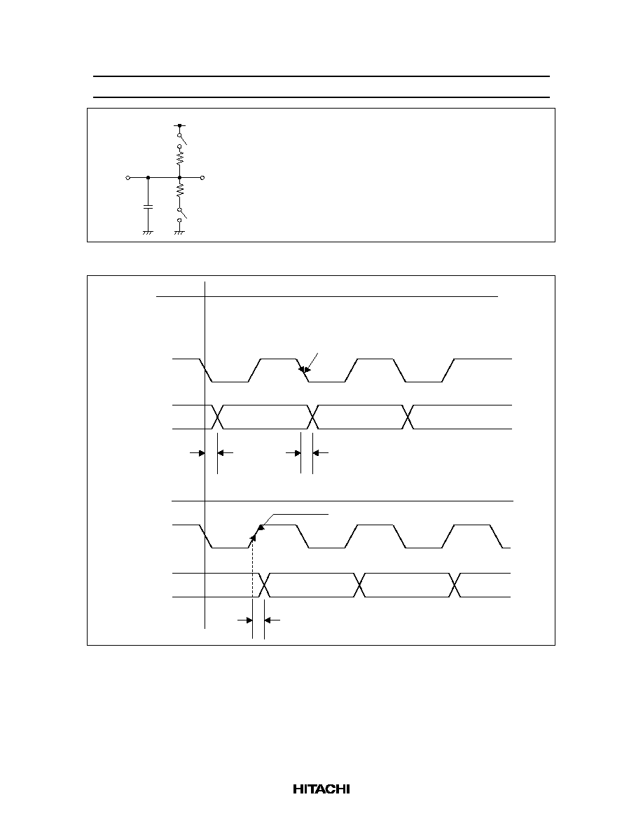
PHASE
(pin 8)
Sample
2
CLK
(pin 7)
Sample
1
Sample
3
B1≠B6,
OF
Data Valid
1
Data Valid
2
Data Valid
3
t
PD
t
PD
CLK
(pin 7)
B1≠B6,
OF
Data Valid
1
Data Valid
2
Data Valid
3
t
PD
Comparator Data is Latched
1
0
1
0
1
0
1
0
PHASE
(pin 8)
1
0
1
0
Sample
1
Sample
2
Sample
3
Comparator Data is Latched
Figure 6 Timing Diagram

HA19216/MP
9
Video Signal
Generator
HA19216
A/D Converter
6
D/A
Converter
TEKTRONIX
520A
Vectorscope
20MHz Clock
Generator
Figure 7 Measuring Circuit for DG and DP
Signal
Generator
HA19216
A/D Converter
6
D/A
Converter
Oscilloscope
20MHz Clock
Generator
Figure 8 Measuring Circuit for Analog Input Frequency Response

HA19216/MP
10
High Frequency Input Response
40IRE Modulated
NTSC Ramp
f
CLK
= 20 Msps Unlocked
Figure 9 High Frequency Analog Input Response Differential Phase
40IRE Modulated
NTSC Ramp
f
CLK
= 20 Msps Unlocked
Figure 10 High Frequency Analog Input Response Differential Gain

HA19216/MP
11
50 mV
2
µ
s
Input (1 Vpp sine wave)
Beat-frequency
wave form of
5.05 MHz input
signal-sampling
at 20 MHz
Figure 11 Beat-Frequency Waveform of 5.05 MHz Input Signal-Sampled at 20 MHz
50 mV
1
µ
s
Input (1 Vpp sine wave)
Beat-frequency
wave form of
10.14 MHz input
signal-sampling
at 20 MHz
Figure 12 Beat-Frequency Waveform of 10.14 MHz Input Signal-Sampled at 20 MHz

HA19216/MP
12
When using this document, keep the following in mind:
1. This document may, wholly or partially, be subject to change without notice.
2. All rights are reserved: No one is permitted to reproduce or duplicate, in any form, the whole or part of
this document without Hitachi's permission.
3. Hitachi will not be held responsible for any damage to the user that may result from accidents or any
other reasons during operation of the user's unit according to this document.
4. Circuitry and other examples described herein are meant merely to indicate the characteristics and
performance of Hitachi's semiconductor products. Hitachi assumes no responsibility for any intellectual
property claims or other problems that may result from applications based on the examples described
herein.
5. No license is granted by implication or otherwise under any patents or other rights of any third party or
Hitachi, Ltd.
6. MEDICAL APPLICATIONS: Hitachi's products are not authorized for use in MEDICAL
APPLICATIONS without the written consent of the appropriate officer of Hitachi's sales company.
Such use includes, but is not limited to, use in life support systems. Buyers of Hitachi's products are
requested to notify the relevant Hitachi sales offices when planning to use the products in MEDICAL
APPLICATIONS.
Hitachi, Ltd.
Semiconductor & IC Div.
Nippon Bldg., 2-6-2, Ohte-machi, Chiyoda-ku, Tokyo 100, Japan
Tel: Tokyo (03) 3270-2111
Fax: (03) 3270-5109
For further information write to:
Hitachi America, Ltd.
Semiconductor & IC Div.
2000 Sierra Point Parkway
Brisbane, CA. 94005-1835
U S A
Tel: 415-589-8300
Fax: 415-583-4207
Hitachi Europe GmbH
Electronic Components Group
Continental Europe
Dornacher Straþe 3
D-85622 Feldkirchen
M¸nchen
Tel: 089-9 91 80-0
Fax: 089-9 29 30 00
Hitachi Europe Ltd.
Electronic Components Div.
Northern Europe Headquarters
Whitebrook Park
Lower Cookham Road
Maidenhead
Berkshire SL6 8YA
United Kingdom
Tel: 0628-585000
Fax: 0628-778322
Hitachi Asia Pte. Ltd.
16 Collyer Quay #20-00
Hitachi Tower
Singapore 0104
Tel: 535-2100
Fax: 535-1533
Hitachi Asia (Hong Kong) Ltd.
Unit 706, North Tower,
World Finance Centre,
Harbour City, Canton Road
Tsim Sha Tsui, Kowloon
Hong Kong
Tel: 27359218
Fax: 27306071