HA22033
GaAs MMIC
Low Noise Amplifier for Micro Wave Application
ADE-207-266 (Z)
1st. Edition
October 1998
Features
∑
Suitable for low noise amplifier of Micro Wave Application(1.5 to 1.9GHz)
∑
Low voltage and low current operation (2.7V, 1.7mA typ.)
∑
Low noise (1.4 dB typ. @1.5GHz)
∑
High power gain (14 dB typ. @1.5GHz)
∑
Built≠in matching circuits (50
)
∑
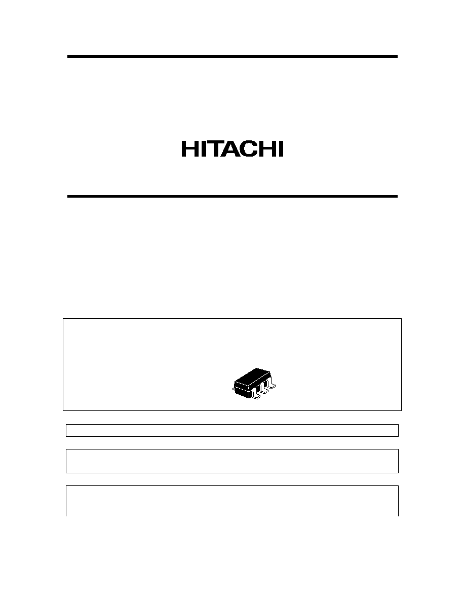
Small surface mount package (MPAK≠5)
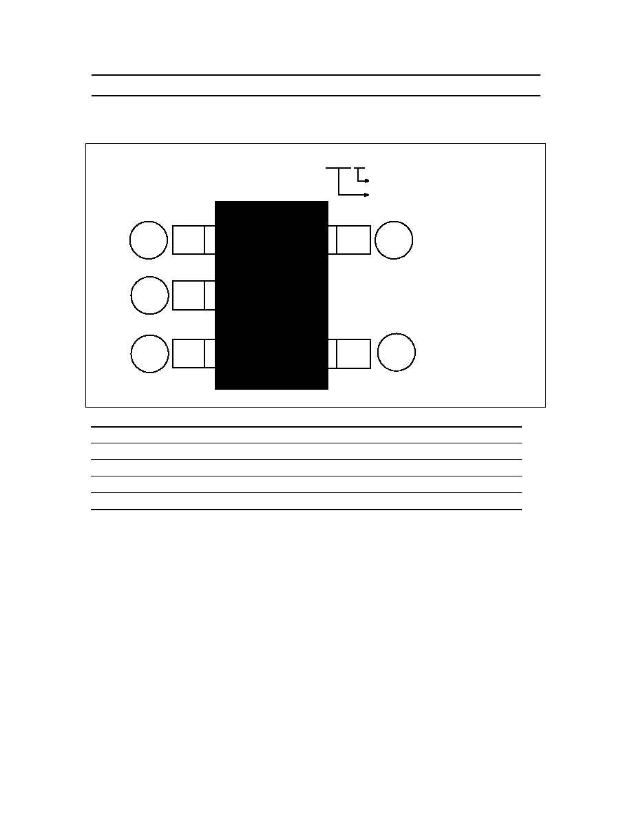
Outline
MPAK≠5
This document may, wholly or partially, be subject to change without notice.
This Device si sensitive to Electro Static Discharge.
An Adequate handling procedure is requested.
CAUTION
This product ues GaAs. Since dust or fume of GaAs is highly poisonous to human body, please do not
treat them mechanically in the manner which might expose to the Aer. And it should never be thrown
out with general industrial or domestic wastes.

HA22033
2
Absolute Maximum Ratings (Ta = 25
∞
C)
Item
Symbol
Ratings
Unit
Supply voltage
Vdd
5
V
Maximum current
Idd
6
mA
Power dissipation
Pd
100
mW
Channel temperature
Tch
150
∞
C
Storage temperature
Tstg
≠55 to +125
∞
C
Operation temperature
Topr
≠20 to +70
∞
C
Maximum input power
Pin max
+15
dBm
Electrical Characteristics (Ta = 25
∞
C, Vdd = 2.7V)
Item
Symbol
Min
Typ
Max
Unit
Test Conditions
Pin
Quiescent current
Idd
--
1.7
2.5
mA
No signal
Power gain
PG
12
14
--
dB
f = 1.5 GHz
Noise figure
NF
--
1.4
2
dB
f = 1.5 GHz
Typical Performance (Ta = 25
∞
C, Vdd = 2.7V)
Item
Symbol
Typ
Unit
Test Conditions
Pin
VSWR (input)
VSWR in
1.5
--
f = 1.5 GHz
4
VSWR (output)
VSWR out
2.2
--
f = 1.5 GHz
1
3rd order intermodulation
distortion
IM3
50
dB
f = 1.5 GHz, Pin = ≠30 dBm