 | –≠–ª–µ–∫—Ç—Ä–æ–Ω–Ω—ã–π –∫–æ–º–ø–æ–Ω–µ–Ω—Ç: HAT2043 | –°–∫–∞—á–∞—Ç—å:  PDF PDF  ZIP ZIP |
HAT2027R
Silicon N Channel Power MOS FET
High Speed Power Switching
ADE-208-458 E (Z)
6th. Edition
February 1999
Features
∑
Low on-resistance
∑
Capable of 2.5 V gate drive
∑
Low drive current
∑
High density mounting
Outline
SOP≠8
1 2
3
4
5
6
7
8
G
D
S
D
G
D
S
D
MOS1
MOS2
1
2
7 8
4
5 6
3
1, 3 Source
2, 4 Gate
5, 6, 7, 8 Drain

HAT2027R
2
Absolute Maximum Ratings (Ta = 25
∞
C)
Item
Symbol
Ratings
Unit
Drain to source voltage
V
DSS
20
V
Gate to source voltage
V
GSS
±
12
V
Drain current
I
D
7
A
Drain peak current
I
D(pulse)
Note1
56
A
Body-drain diode reverse drain current
I
DR
7
A
Channel dissipation
Pch
Note2
2
W
Channel dissipation
Pch
Note3
3
W
Channel temperature
Tch
150
∞
C
Storage temperature
Tstg
≠ 55 to + 150
∞
C
Note:
1. PW
10
µ
s, duty cycle
1 %
2. 1 Drive operation : When using the glass epoxy board (FR4 40 x 40 x 1.6 mm), PW
10s
3. 2 Drive operation : When using the glass epoxy board (FR4 40 x 40 x 1.6 mm), PW
10s
Electrical Characteristics (Ta = 25
∞
C)
Item
Symbol Min
Typ
Max
Unit
Test Conditions
Drain to source breakdown voltage V
(BR)DSS
20
--
--
V
I
D
= 10 mA, V
GS
= 0
Gate to source breakdown voltage V
(BR)GSS
±
12
--
--
V
I
G
=
±
100
µ
A, V
DS
= 0
Gate to source leak current
I
GSS
--
--
±
10
µ
A
V
GS
=
±
10 V, V
DS
= 0
Zero gate voltege drain current
I
DSS
--
--
10
µ
A
V
DS
= 20 V, V
GS
= 0
Gate to source cutoff voltage
V
GS(off)
0.5
--
1.5
V
V
DS
= 10 V,
I
D
= 1 mA
Static drain to source on state
R
DS(on)
--
0.03
0.038
I
D
= 4 A, V
GS
= 4 V
Note4
resistance
R
DS(on)
--
0.038
0.053
I
D
= 4 A, V
GS
= 2.5 V
Note4
Forward transfer admittance
|y
fs
|
9
14
--
S
I
D
= 4 A, V
DS
= 10 V
Note4
Input capacitance
Ciss
--
720
--
pF
V
DS
= 10 V
Output capacitance
Coss
--
450
--
pF
V
GS
= 0
Reverse transfer capacitance
Crss
--
185
--
pF
f = 1MHz
Turn-on delay time
t
d(on)
--
28
--
ns
V
GS
= 4 V, I
D
= 4 A
Rise time
t
r
--
145
--
ns
V
DD
10 V
Turn-off delay time
t
d(off)
--
100
--
ns
Fall time
t
f
--
125
--
ns
Body≠drain diode forward voltage
V
DF
--
0.9
1.4
V
IF = 7 A, V
GS
= 0
Note4
Body≠drain diode reverse
recovery time
t
rr
--
60
--
ns
IF = 7 A, V
GS
= 0
diF/ dt = 20 A/
µ
s
Note:
4. Pulse test
HAT2027R
3
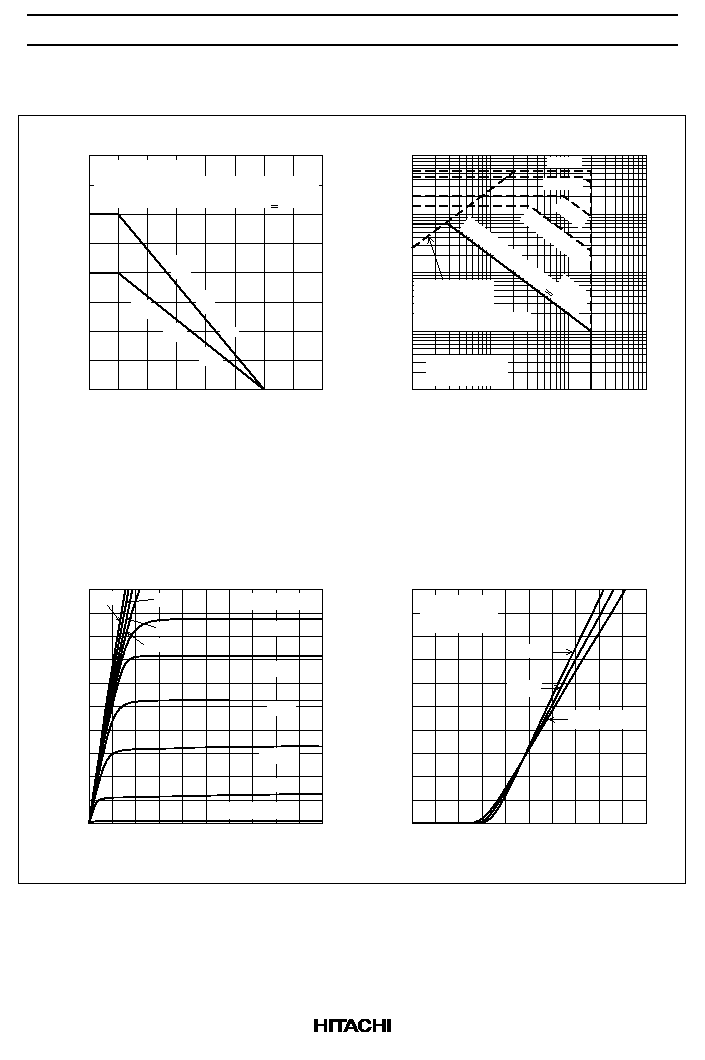
Main Characteristics
4.0
3.0
2.0
1.0
0
50
100
150
200
100
30
10
3
1
0.3
0.1
0.03
0.01
0.1
0.3
1
3
10
30
100
50
40
30
20
10
0
2
4
6
8
10
10V
6 V
5 V
4.5 V
50
40
30
20
10
0
1
2
3
4
5
Tc = 75∞C
25∞C
≠25∞C
Ta = 25 ∞C
1 shot Pulse
1 ms
PW = 10 ms
10 µs
100 µs
4 V
3.5 V
3 V
2.5 V
2 V
V = 1.5 V
GS
Channel Dissipation Pch (W)
Ambient Temperature Ta (∞C)
Power vs. Temperature Derating
2 Drive Operation
1 Drive Operation
Drain to Source Voltage V (V)
DS
Drain Current I (A)
D
Maximum Safe Operation Area
Operation in
this area is
limited by R
DS(on)
Drain to Source Voltage V (V)
DS
Drain Current I (A)
D
Typical Output Characteristics
Pulse Test
Gate to Source Voltage V (V)
GS
Drain Current I (A)
D
Typical Transfer Characteristics
V = 10 V
Pulse Test
DS
Test Condition :
When using the glass epoxy board
(FR4 40x40x1.6 mm), PW < 10 s
Note 5 :
When using the glass epoxy board
(FR4 40x40x1.6 mm)
Note 5
DC Operation (PW < 10 s)
HAT2027R
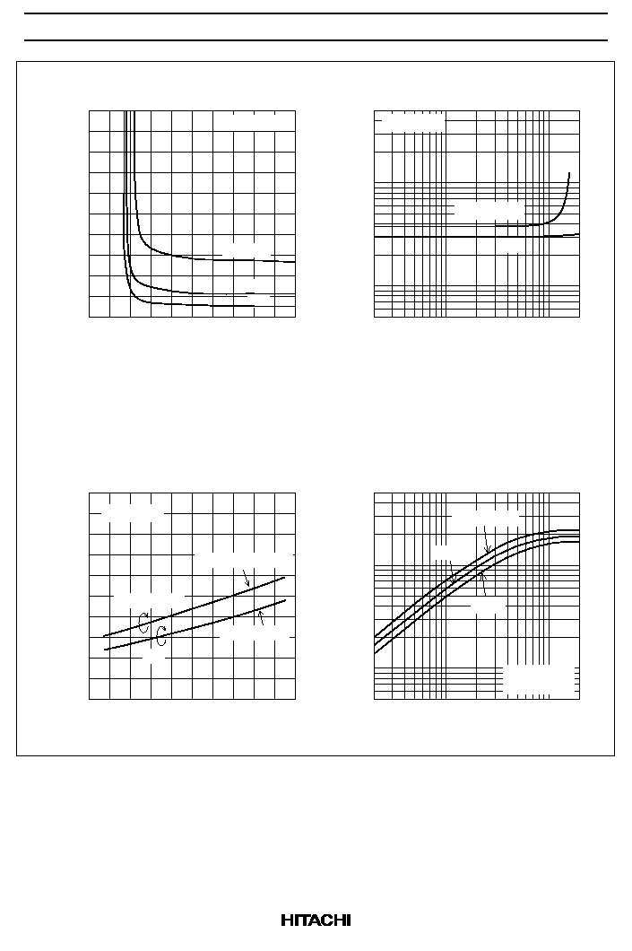
4
0.5
0.4
0.3
0.2
0.1
0
2
4
6
8
10
I = 5 A
D
1 A
2 A
0.5
0.2
0.05
0.1
0.02
0.005
0.01
0.2
0.5
1
2
5
10
20
0.10
0.08
0.06
0.04
0.02
≠40
0
40
80
120
160
0
50
20
10
2
5
1
0.5
0.2
0.5
1
2
5
10
20
25 ∞C
Tc = ≠25 ∞C
75 ∞C
Gate to Source Voltage V (V)
GS
Drain to Source Voltage V (V)
DS(on)
Drain to Source Saturation Voltage vs.
Gate to Source Voltage
Pulse Test
Drain Current I (A)
D
Drain to Source On State Resistance
R ( )
DS(on)
Static Drain to Source on State Resistance
vs. Drain Current
Pulse Test
Case Temperature Tc (∞C)
R ( )
DS(on)
Static Drain to Source on State Resistance
Pulse Test
Static Drain to Source on State Resistance
vs. Temperature
Forward Transfer Admittance |yfs| (S)
Drain Current I (A)
D
Forward Transfer Admittance vs.
Drain Current
DS
V = 10 V
Pulse Test
0
I = 1 A, 2 A, 5 A
D
1 A, 2 A, 5 A
V = 2.5 V
GS
4 V
V = 2.5 V
GS
4 V
HAT2027R
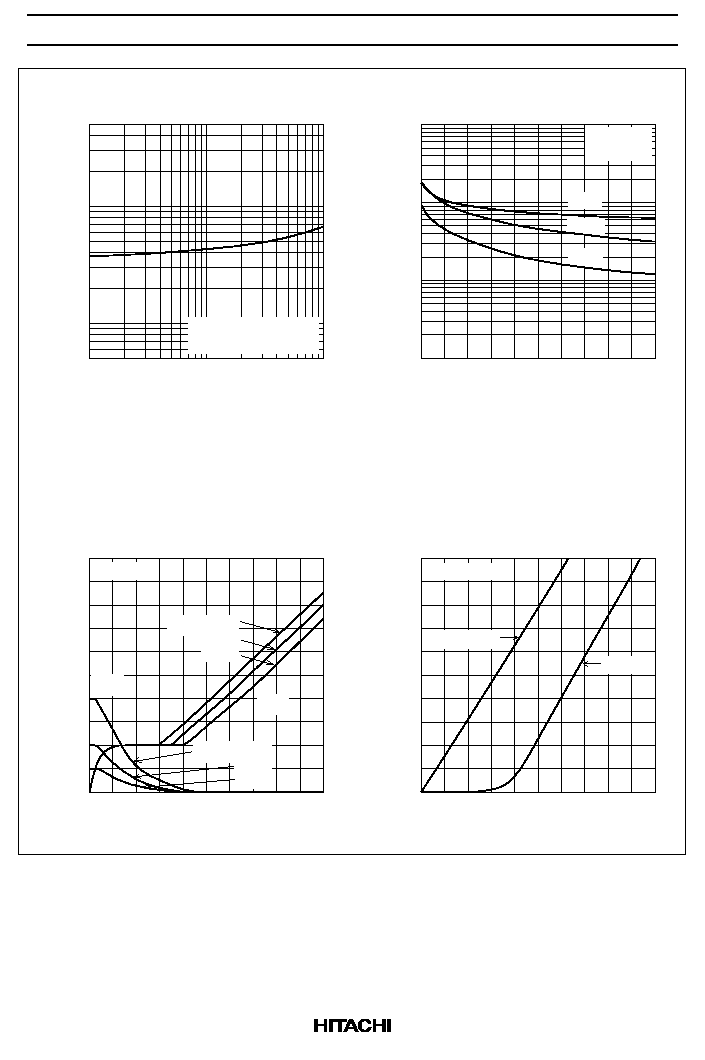
5
0.2
0.5
1
2
5
10
0.1
500
200
100
20
50
10
5
0
4
8
12
16
20
10000
3000
1000
300
100
30
10
Ciss
Coss
Crss
V = 0
f = 1 MHz
GS
50
40
30
20
10
0
10
8
6
4
2
4
8
12
16
20
0
di/dt = 20 A/µs
V = 0, Ta = 25∞C
GS
V
GS
V
DS
I = 7 A
D
V = 5 V
10 V
20 V
DD
V = 20 V
10 V
5 V
DD
Reverse Drain Current I (A)
DR
Reverse Recovery Time trr (ns)
Body≠Drain Diode Reverse
Recovery Time
Capacitance C (pF)
Drain to Source Voltage V (V)
DS
Typical Capacitance vs.
Drain to Source Voltage
Gate Charge Qg (nc)
Drain to Source Voltage V (V)
DS
Gate to Source Voltage V (V)
GS
Dynamic Input Characteristics
50
40
30
20
10
0
0.4
0.8
1.2
1.6
2.0
0, ≠5 V
V = 5 V
GS
Source to Drain Voltage V (V)
SD
Reverse Drain Current I (A)
DR
Reverse Drain Current vs.
Souece to Drain Voltage
Pulse Test