HB56SW3272ESK-5/6
256MB Buffered EDO DRAM DIMM
32-Mword
◊
72-bit, 4k Refresh, 2 Bank Module
(36 pcs of 16M
◊
4 components)
ADE-203-872B (Z)
Rev. 1.0
June 23, 1998
Description
The HB56SW3272ESK belong to 8-byte DIMM (Dual in-line Memory Module) family , and have been
developed an optimized main memory solution for 4 and 8-byte processor applications. The
HB56SW3272ESK is 32 M
◊
72 Dynamic RAM Module, mounted 36 pieces of 64-Mbit DRAM
(HM5165405) sealed in TCP package and 2 pieces of 16-bit BiCMOS line driver sealed in TSSOP
package. The HB56SW3272ESK offer Extended Data Out (EDO) Page Mode as a high speed access
mode. An outline of the HB56SW3272ESK are 168-pin socket type package (dual lead out). Therefore, the
HB56SW3272ESK make high density mounting possible without surface mount technology. The
HB56SW3272ESK provide common data inputs and outputs. Decoupling capacitors are mounted beside
each TCP on its module board.
Note:
Do not push the cover or drop the modules in order to protect from mechanical defects, which
would be electrical defects.
Features
∑
168-pin socket type package (Dual lead out)
Lead pitch : 1.27 mm
∑
Single 3.3 V supply (
±
0.3 V)
∑
High speed
Access time: t
RAC
= 50 ns/60 ns (max)
Access time: t
CAC
= 18 ns/20 ns (max)
∑
Low power dissipation
Active mode: 8.78 W/7.49 W (max)
Standby mode (TTL): 295.2 mW (max)
∑
JEDEC standard outline buffered 8-byte DIMM
∑
Buffered input except RAS and DQ
HB56SW3272ESK-5/6
2
∑
4-byte interleave enabled, dual address input (A0/B0)
∑
EDO page mode capability
∑
4096 refresh cycles: 64 ms
∑
2 variations of refresh
RAS-only refresh
CAS-before-RAS refresh
Ordering Information
Type No.
Access time
Package
Contact pad
HB56SW3272ESK-5
HB56SW3272ESK-6
50 ns
60 ns
168-pin dual lead out
socket type
Gold
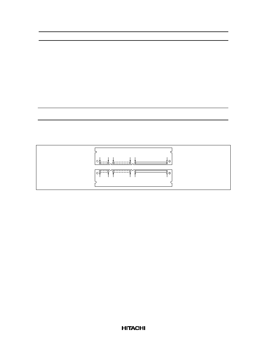
Pin Arrangement
1 pin 10 pin 11 pin
40 pin 41 pin
84 pin
85 pin 94 pin 95 pin 124 pin 125 pin
168 pin

HB56SW3272ESK-5/6
3
Pin No.
Signal name Pin No.
Signal name Pin No.
Signal name Pin No.
Signal name
1
V
SS
43
V
SS
85
V
SS
127
V
SS
2
DQ0
44
OE
2
86
DQ36
128
NC
3
DQ1
45
RE
2
87
DQ37
129
RE
3
4
DQ2
46
CE
4
88
DQ38
130
CE
5
5
DQ3
47
NC
89
DQ39
131
NC
6
V
CC
48
WE
2
90
V
CC
132
PDE
7
DQ4
49
V
CC
91
DQ40
133
V
CC
8
DQ5
50
NC
92
DQ41
134
NC
9
DQ6
51
NC
93
DQ42
135
NC
10
DQ7
52
DQ18
94
DQ43
136
DQ54
11
DQ8
53
DQ19
95
DQ44
137
DQ55
12
V
SS
54
V
SS
96
V
SS
138
V
SS
13
DQ9
55
DQ20
97
DQ45
139
DQ56
14
DQ10
56
DQ21
98
DQ46
140
DQ57
15
DQ11
57
DQ22
99
DQ47
141
DQ58
16
DQ12
58
DQ23
100
DQ48
142
DQ59
17
DQ13
59
V
CC
101
DQ49
143
V
CC
18
V
CC
60
DQ24
102
V
CC
144
DQ60
19
DQ14
61
NC
103
DQ50
145
NC
20
DQ15
62
NC
104
DQ51
146
NC
21
DQ16
63
NC
105
DQ52
147
NC
22
DQ17
64
NC
106
DQ53
148
NC
23
V
SS
65
DQ25
107
V
SS
149
DQ61
24
NC
66
DQ26
108
NC
150
DQ62
25
NC
67
DQ27
109
NC
151
DQ63
26
V
CC
68
V
SS
110
V
CC
152
V
SS
27
WE
0
69
DQ28
111
NC
153
DQ64
28
CE
0
70
DQ29
112
CE
1
154
DQ65
29
NC
71
DQ30
113
NC
155
DQ66
30
RE
0
72
DQ31
114
RE
1
156
DQ67
31
OE
0
73
V
CC
115
NC
157
V
CC
32
V
SS
74
DQ32
116
V
SS
158
DQ68
33
A0
75
DQ33
117
A1
159
DQ69
34
A2
76
DQ34
118
A3
160
DQ70
35
A4
77
DQ35
119
A5
161
DQ71
HB56SW3272ESK-5/6
4
Pin Arrangement (cont)
Pin No.
Signal name Pin No.
Signal name Pin No.
Signal name Pin No.
Signal name
36
A6
78
V
SS
120
A7
162
V
SS
37
A8
79
PD1
121
A9
163
PD2
38
A10
80
PD3
122
A11
164
PD4
39
NC
81
PD5
123
NC
165
PD6
40
V
CC
82
PD7
124
V
CC
166
PD8
41
NC
83
ID0 (V
SS
)
125
NC
167
ID1 (V
SS
)
42
NC
84
V
CC
126
B0
168
V
CC
Pin Description
Pin name
Function
A0 to A11, B0
Address input
Row address (D0 to D35)
A0 to A11, B0
Column address (D0 to D35)
A0 to A11, B0
Refresh address (D0 to D35)
A0 to A11, B0
DQ0 to DQ71
Data input/output
RE
0 to
RE
3
Row address strobe (
RAS
)
CE
0,
CE
1,
CE
4,
CE
5
Column address strobe (
CAS
)
WE
0,
WE
2
Read/Write enable
OE
0,
OE
2
Output enable
PD1 to PD8
Presence detect
ID0 , ID1
ID bit
PDE
Presence detect enable
V
CC
Power supply
V
SS
Ground
NC
No connection
HB56SW3272ESK-5/6
5
Presence Detect Pin Assignment (Controlled by PDE pin)
PDE
= Low
PDE
= High
Pin name
Pin No.
50 ns
60ns
All
PD1
79
1
1
High-Z
PD2
163
0
0
High-Z
PD3
80
0
0
High-Z
PD4
164
0
0
High-Z
PD5
81
1
1
High-Z
PD6
165
0
1
High-Z
PD7
82
0
1
High-Z
PD8
166
0
0
High-Z
Note: 1: High level (driver output). 0: Low level (driver output)
HB56SW3272ESK-5/6
6
Block Diagram
A0
D0 to D8 , D18 to D26
A1 to A11
D0 to D35
B0
D9 to D17 , D27 to D35
Capacitor
◊
20 pcs
D0 to D35, 16-bit driver
D0 to D35, 16-bit driver
PD1 to PD8
PD1 to PD8
V
SS or
V
CC
RE
0
CE
0
WE
0
OE
0
D0
DQ0
DQ1
DQ2
DQ3
DQ4
DQ5
DQ6
DQ7
DQ8
DQ9
DQ10
DQ11
DQ12
DQ13
DQ14
DQ15
DQ16
DQ17
DQ18
DQ19
DQ20
DQ21
DQ22
DQ23
DQ24
DQ25
DQ26
DQ27
DQ28
DQ29
DQ30
DQ31
D1
D2
D3
D4
D5
D6
D7
DQ32
DQ33
DQ34
DQ35
D8
I/O
I/O
I/O
I/O
I/O
I/O
I/O
I/O
I/O
I/O
I/O
I/O
I/O
I/O
I/O
I/O
I/O
I/O
I/O
I/O
I/O
I/O
I/O
I/O
I/O
I/O
I/O
I/O
I/O
I/O
I/O
I/O
I/O
I/O
I/O
I/O
D18
CAS RAS WE OE
CAS RAS WE OE
CAS RAS WE OE
CAS RAS WE OE
CAS RAS WE OE
CAS RAS WE OE
CAS RAS WE OE
CAS RAS WE OE
CAS RAS WE OE
CAS RAS WE OE
CAS RAS WE OE
CAS RAS WE OE
CAS RAS WE OE
CAS RAS WE OE
CAS RAS WE OE
CAS RAS WE OE
CAS RAS WE OE
CAS RAS WE OE
CAS RAS WE OE
CAS RAS WE OE
CAS RAS WE OE
CAS RAS WE OE
CAS RAS WE OE
CAS RAS WE OE
CAS RAS WE OE
CAS RAS WE OE
CAS RAS WE OE
CAS RAS WE OE
CAS RAS WE OE
CAS RAS WE OE
CAS RAS WE OE
CAS RAS WE OE
CAS RAS WE OE
CAS RAS WE OE
CAS RAS WE OE
CAS RAS WE OE
D19
D20
D21
D22
D23
D24
D25
D26
I/O
I/O
I/O
I/O
I/O
I/O
I/O
I/O
I/O
I/O
I/O
I/O
I/O
I/O
I/O
I/O
I/O
I/O
I/O
I/O
I/O
I/O
I/O
I/O
I/O
I/O
I/O
I/O
I/O
I/O
I/O
I/O
I/O
I/O
I/O
I/O
RE
2
CE
4
WE
2
OE
2
D9
D10
D11
D12
D13
D14
D15
D16
DQ36
DQ37
DQ38
DQ39
DQ40
DQ41
DQ42
DQ43
DQ44
DQ45
DQ46
DQ47
DQ48
DQ49
DQ50
DQ51
DQ52
DQ53
DQ54
DQ55
DQ56
DQ57
DQ58
DQ59
DQ60
DQ61
DQ62
DQ63
DQ64
DQ65
DQ66
DQ67
DQ68
DQ69
DQ70
DQ71
D17
I/O
I/O
I/O
I/O
I/O
I/O
I/O
I/O
I/O
I/O
I/O
I/O
I/O
I/O
I/O
I/O
I/O
I/O
I/O
I/O
I/O
I/O
I/O
I/O
I/O
I/O
I/O
I/O
I/O
I/O
I/O
I/O
I/O
I/O
I/O
I/O
D27
D28
D29
D30
D31
D32
D33
D34
D35
I/O
I/O
I/O
I/O
I/O
I/O
I/O
I/O
I/O
I/O
I/O
I/O
I/O
I/O
I/O
I/O
I/O
I/O
I/O
I/O
I/O
I/O
I/O
I/O
I/O
I/O
I/O
I/O
I/O
I/O
I/O
I/O
I/O
I/O
I/O
I/O
RE
1
RE
3
CE
1
CE
5
V
CC
V
SS
* D0 to D35 : HM5165405
: 16-bit driver
HB56SW3272ESK-5/6
7
Absolute Maximum Ratings
Parameter
Symbol
Value
Unit
Terminal voltage on any pin relative to V
SS
V
T
≠0.5 to +4.6
V
Power supply voltage relative to V
SS
V
CC
≠0.5 to +4.6
V
Short circuit output current
Iout
50
mA
Power dissipation
P
T
19
W
Storage temperature range
Tstg
≠55 to +125
∞
C
DC Operating Conditions
Parameter
Symbol
Min
Typ
Max
Unit
Notes
Supply voltage
V
CC
3.0
3.3
3.6
V
1, 2
V
SS
0
0
0
V
2
Input high voltage
V
IH
2.0
--
V
CC
+ 0.3
V
1
Input low voltage
V
IL
≠0.3
--
0.8
V
1
Ambient temperature range
Ta
0
--
70
∞
C
Ambient illuminance
--
--
--
100
lx
Notes: 1. All voltage referred to V
SS
.
2. The supply voltage with all V
CC
pins must be on the same level. The supply voltage with all V
SS
pins must be on the same level.
HB56SW3272ESK-5/6
8
DC Characteristics
50 ns
60 ns
Parameter
Symbol Min
Max
Min
Max
Unit
Test conditions
Operating current*
1
, *
2
I
CC1
--
2440
--
2080
mA
t
RC
= min
Standby current
I
CC2
--
82
--
82
mA
TTL interface
RAS
,
CAS
= V
IH
Dout = High-Z
--
28
--
28
mA
CMOS interface
RAS
,
CAS
V
CC
≠ 0.2 V
Dout = High-Z
RAS
-only refresh current*
2
I
CC3
--
2440
--
2080
mA
t
RC
= min
Standby current*
1
I
CC5
--
190
--
190
mA
RAS
= V
IH
,
CAS
= V
IL
Dout = enable
CAS
-before-
RAS
refresh
current
I
CC6
--
2440
--
2080
mA
t
RC
= min
EDO page mode current*
1,
*
3
I
CC7
--
2080
--
1900
mA
RAS
= V
IL
,
CAS
cycle,
t
HPC
= t
HPC
min
Input leakage current
I
LI
≠10
10
≠10
10
µ
A
0 V
Vin
V
CC
+ 0.3 V
Output leakage current
I
LO
≠10
10
≠10
10
µ
A
0 V
Vout
V
CC
Dout = disable
Output high voltage
V
OH
2.4
V
CC
2.4
V
CC
V
High Iout = ≠2 mA
Output low voltage
V
OL
0
0.4
0
0.4
V
Low Iout = 2 mA
Notes : 1. I
CC
depends on output load condition when the device is selected. I
CC
max is specified at the
output open condition.
2. Address can be changed once or less while
RAS
= V
IL
.
3. Measured with one sequential address change per EDO cycle, t
HPC
.
Capacitance (Ta = 25
∞
C, V
CC
= 3.3 V
±
0.3 V)
Parameter
Symbol
Typ
Max
Unit
Notes
Input capacitance (Address)
C
I1
--
20
pF
1
Input capacitance (
CAS
,
WE
,
OE
)
C
I2
--
20
pF
1
Input capacitance (
RAS
)
C
I3
--
78
pF
1
I/O capacitance (DQ)
C
I/O
--
27
pF
1, 2
Notes : 1. Capacitance measured with Boonton Meter or effective capacitance measuring method.
2.
CAS
= V
IH
to disable Dout.
HB56SW3272ESK-5/6
9
AC Characteristics (Ta = 0 to +70
∞
C, V
CC
= 3.3 V
±
0.3 V, V
SS
= 0 V) *
1
, *
2
, *
19
Test Conditions
∑
Input rise and fall time: 2 ns
∑
Input levels: V
IL
= 0 V, V
IH
= 3 V
∑
Input timing reference levels: 0.8 V, 2.0 V
∑
Output timing reference levels: 0.8 V, 2.0 V
∑
Output load: 1 TTL gate + C
L
(100 pF) (Including scope and jig)
∑
Ambient illuminance: Under 100 lx
Read, Write, Read-Modify-Write and Refresh Cycles (Common parameters)
50 ns
60 ns
Parameter
Symbol Min
Max
Min
Max
Unit
Notes
Random read or write cycle time
t
RC
84
--
104
--
ns
RAS
precharge time
t
RP
30
--
40
--
ns
CAS
precharge time
t
CP
8
--
10
--
ns
RAS
pulse width
t
RAS
50
10000
60
10000
ns
CAS
pulse width
t
CAS
8
10000
10
10000
ns
Row address setup time
t
ASR
5
--
5
--
ns
Row address hold time
t
RAH
8
--
10
--
ns
Column address setup time
t
ASC
0
--
0
--
ns
Column address hold time
t
CAH
8
--
10
--
ns
RAS
to
CAS
delay time
t
RCD
12
32
14
40
ns
3
RAS
to column address delay time
t
RAD
10
20
12
25
ns
4
RAS
hold time
t
RSH
18
--
20
--
ns
CAS
hold time
t
CSH
35
--
40
--
ns
CAS
to
RAS
precharge time
t
CRP
10
--
10
--
ns
OE
to Din delay time
t
OED
18
--
20
--
ns
5
OE
delay time from Din
t
DZO
0
--
0
--
ns
6
CAS
delay time from Din
t
DZC
0
--
0
--
ns
6
Transition time (rise and fall)
t
T
2
50
2
50
ns
7

HB56SW3272ESK-5/6
10
Read Cycle
50 ns
60 ns
Parameter
Symbol Min
Max
Min
Max
Unit
Notes
Access time from
RAS
t
RAC
--
50
--
60
ns
8, 9
Access time from
CAS
t
CAC
--
18
--
20
ns
9, 10, 17
Access time from address
t
AA
--
30
--
35
ns
9, 11, 17
Access time from
OE
t
OEA
--
18
--
20
ns
9
Read command setup time
t
RCS
0
--
0
--
ns
Read command hold time to
CAS
t
RCH
0
--
0
--
ns
12
Read command hold time from
RAS
t
RCHR
50
--
60
--
ns
Read command hold time to
RAS
t
RRH
0
--
0
--
ns
12
Column address to
RAS
lead time
t
RAL
30
--
35
--
ns
Column address to
CAS
lead time
t
CAL
15
--
18
--
ns
CAS
to output in low-Z
t
CLZ
2
--
2
--
ns
Output data hold time
t
OH
3
--
3
--
ns
21
Output data hold time from
OE
t
OHO
3
--
3
--
ns
Output buffer turn-off time
t
OFF
--
18
--
20
ns
13, 21
Output buffer turn-off to
OE
t
OEZ
--
18
--
20
ns
13
CAS
to Din delay time
t
CDD
18
--
20
--
ns
5
Output data hold time from
RAS
t
OHR
3
--
3
--
ns
21
Output buffer turn-off to
RAS
t
OFR
--
13
--
15
ns
13, 21
Output buffer turn-off to
WE
t
WEZ
--
18
--
20
ns
13
WE
to Din delay time
t
WED
18
--
20
--
ns
RAS
to Din delay time
t
RDD
13
--
15
--
ns
Write Cycle
50 ns
60 ns
Parameter
Symbol Min
Max
Min
Max
Unit
Notes
Write command setup time
t
WCS
0
--
0
--
ns
14
Write command hold time
t
WCH
8
--
10
--
ns
Write command pulse width
t
WP
8
--
10
--
ns
Write command to
RAS
lead time
t
RWL
18
--
20
--
ns
Write command to
CAS
lead time
t
CWL
8
--
10
--
ns
Data-in setup time
t
DS
0
--
0
--
ns
15
Data-in hold time
t
DH
13
--
15
--
ns
15

HB56SW3272ESK-5/6
11
Read-Modify-Write Cycle
50 ns
60 ns
Parameter
Symbol Min
Max
Min
Max
Unit
Notes
Read-modify-write cycle time
t
RWC
116
--
140
--
ns
RAS
to
WE
delay time
t
RWD
72
--
84
--
ns
14
CAS
to
WE
delay time
t
CWD
30
--
34
--
ns
14
Column address to
WE
delay time
t
AWD
42
--
49
--
ns
14
OE
hold time from
WE
t
OEH
13
--
15
--
ns
Refresh Cycle
50 ns
60 ns
Parameter
Symbol Min
Max
Min
Max
Unit
Notes
CAS
setup time (CBR refresh cycle)
t
CSR
10
--
10
--
ns
CAS
hold time (CBR refresh cycle)
t
CHR
8
--
10
--
ns
WE
setup time (CBR refresh cycle)
t
WRP
5
--
5
--
ns
WE
hold time (CBR refresh cycle)
t
WRH
10
--
10
--
ns
RAS
precharge to
CAS
hold time
t
RPC
5
--
5
--
ns
EDO Page Mode Cycle
50 ns
60 ns
Parameter
Symbol Min
Max
Min
Max
Unit
Notes
EDO page mode cycle time
t
HPC
20
--
25
--
ns
20
EDO page mode
RAS
pulse width
t
RASP
--
100000 --
100000 ns
16
Access time from
CAS
precharge
t
CPA
--
33
--
40
ns
9, 17
RAS
hold time from
CAS
precharge
t
CPRH
33
--
40
--
ns
Output data hold time from
CAS
low
t
DOH
3
--
3
--
ns
9, 22
CAS
hold time referred
OE
t
COL
8
--
10
--
ns
CAS
to
OE
setup time
t
COP
5
--
5
--
ns
Read command hold time from
CAS
precharge
t
RCHC
28
--
35
--
ns
Write pulse width during
CAS
precharge
t
WPE
8
--
10
--
ns
OE
precharge time
t
OEP
8
--
10
--
ns
HB56SW3272ESK-5/6
12
EDO Page Mode Read-Modify-Write Cycle
50 ns
60 ns
Parameter
Symbol Min
Max
Min
Max
Unit
Notes
EDO page mode read- modify-write
cycle time
t
HPRWC
57
--
68
--
ns
WE
delay time from
CAS
precharge
t
CPW
45
--
54
--
ns
14
Refresh
Parameter
Symbol
Max
Unit
Notes
Refresh period
t
REF
64
ms
4096 cycles
Notes: 1. AC measurements assume t
T
= 2 ns.
2. An initial pause of 200
µ
s is required after power up followed by a minimum of eight initialization
cycles (any combination of cycles containing
RAS
-only refresh or
CAS
-before-
RAS
refresh).
3. Operation with the t
RCD
(max) limit insures that t
RAC
(max) can be met, t
RCD
(max) is specified as a
reference point only; if t
RCD
is greater than the specified t
RCD
(max) limit, than the access time is
controlled exclusively by t
CAC
.
4. Operation with the t
RAD
(max) limit insures that t
RAC
(max) can be met, t
RAD
(max) is specified as a
reference point only; if t
RAD
is greater than the specified t
RAD
(max) limit, then access time is
controlled exclusively by t
AA
.
5. Either t
OED
or t
CDD
must be satisfied.
6. Either t
DZO
or t
DZC
must be satisfied.
7. V
IH
(min) and V
IL
(max) are reference levels for measuring timing of input signals. Also, transition
times are measured between V
IH
(min) and V
IL
(max).
8. Assumes that t
RCD
t
RCD
(max) and t
RAD
t
RAD
(max). If t
RCD
or t
RAD
is greater than the maximum
recommended value shown in this table, t
RAC
exceeds the value shown.
9. Measured with a load circuit equivalent to 1 TTL loads and 100 pF.
10. Assumes that t
RCD
t
RCD
(max) and t
RCD
+ t
CAC
(max)
t
RAD
+ t
AA
(max).
11. Assumes that t
RAD
t
RAD
(max) and t
RCD
+ t
CAC
(max)
t
RAD
+ t
AA
(max).
12. Either t
RCH
or t
RRH
must be satisfied for a read cycles.
13. t
OFF
(max), t
OEZ
(max), t
WEZ
(max) and t
OFR
(max) define the time at which the outputs achieve the
open circuit condition and are not referred to output voltage levels.
14. t
WCS
, t
RWD
, t
CWD
, t
AWD
and t
CPW
are not restrictive operating parameters. They are included in the
data sheet as electrical characteristics only; if t
WCS
t
WCS
(min), the cycle is an early write cycle
and the data out pin will remain open circuit (high impedance) throughout the entire cycle; if t
RWD
t
RWD
(min), t
CWD
t
CWD
(min), and t
AWD
t
AWD
(min), or t
CWD
t
CWD
(min), t
AWD
t
AWD
(min) and t
CPW
t
CPW
(min), the cycle is a read-modify-write and the data output will contain data read from the
selected cell; if neither of the above sets of conditions is satisfied, the condition of the data out
(at access time) is indeterminate.
15. t
DS
and t
DH
are referred to
CAS
leading edge in early write cycles and to
WE
leading edge in
delayed write or read-modify-write cycles.
16. t
RASP
defines
RAS
pulse width in EDO page mode cycles.
17. Access time is determined by the longest among t
AA
, t
CAC
and t
CPA
.
18. In delayed write or read-modify-write cycles,
OE
must disable output buffer prior to applying data
to the device.

HB56SW3272ESK-5/6
13
19. When output buffers are enabled once, sustain the low impedance state until valid data is
obtained. When output buffer is turned on and off within a very short time, generally it causes
large V
CC
/V
SS
line noise, which causes to degrade V
IH
min/V
IL
max level.
20. t
HPC
(min) can be achieved during a series of EDO page mode write cycles or EDO page mode
read cycles. If both write and read operation are mixed in a EDO page mode
RAS
cycle (EDO
page mode mix cycle (1), (2)), minimum value of
CAS
cycle (t
CAS
+ t
CP
+ 2 t
T
) becomes greater
than the specified t
HPC
(min) value. The value of
CAS
cycle time of mixed EDO page mode is
shown in EDO page mode mix cycle (1) and (2).
21. Data output turns off and becomes high impedance from later rising edge of
RAS
and
CAS
.
Hold time and turn off time are specified by the timing specifications of later rising edge of
RAS
and
CAS
between t
OHR
and t
OH
and between t
OFR
and t
OFF
.
22. t
DOH
defines the time at which the output level go cross. V
OL
= 0.8 V, V
OH
= 2.0 V of output timing
reference level.
23. XXX: H or L (H: V
IH
(min)
V
IN
V
IH
(max), L: V
IL
(min)
V
IN
V
IL
(max))
///////: Invalid Dout
When the address, clock and input pins are not described on timing waveforms, their pins must
be applied V
IH
or V
IL
.
HB56SW3272ESK-5/6
14
Timing Waveforms*
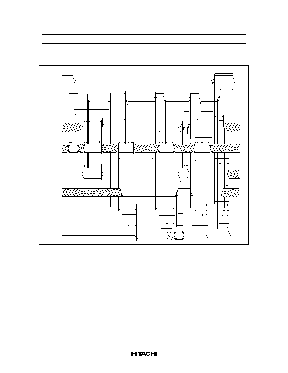
23
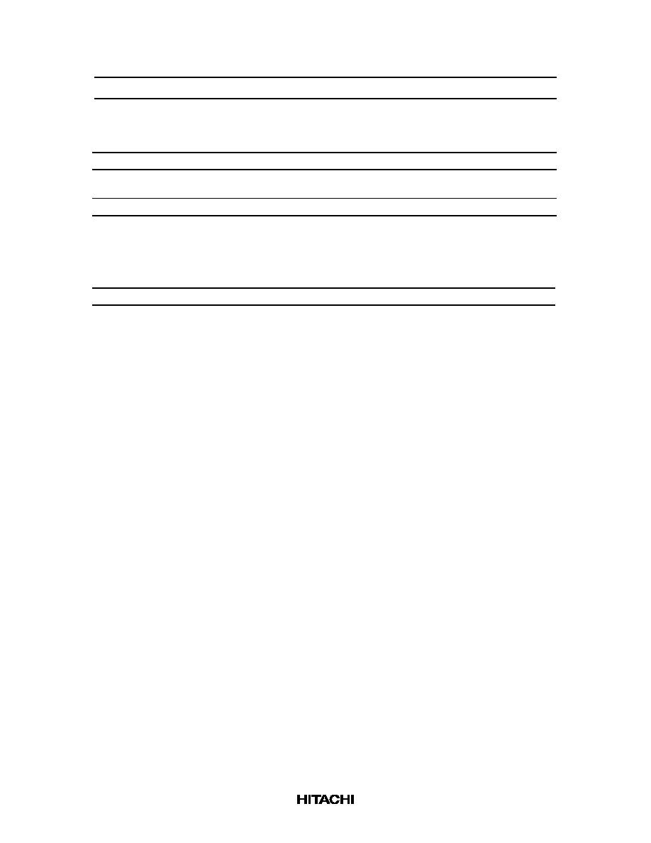
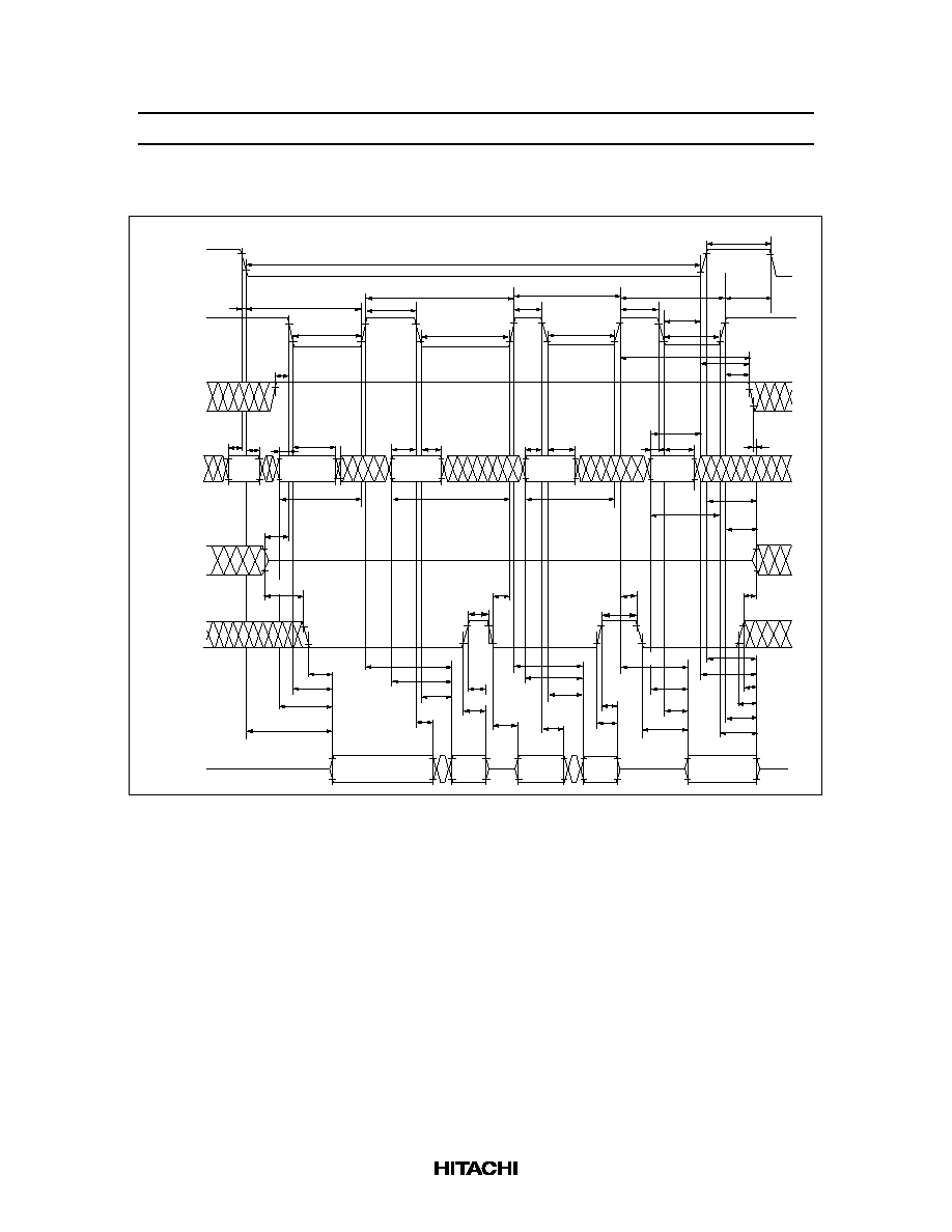
Read Cycle
RAS
Address
WE
Dout
OE
Din
t
RC
Row
Column
t
RCS
t
RCH
t
CDD
t
DZC
High-Z
Dout
t
DZO
t
OED
t
RAC
t
OEA
t
AA
t
CAC
t
CLZ
t
OH
t
OFF
t
OHO
t
OEZ
CAS
t
RDD
t
WED
t
OFR
t
OHR
t
WEZ
t
RAS
t
CAS
t
RP
t
CSH
t
RCD
t
RSH
t
CRP
t
T
t
RAD
t
RAL
t
CAL
t
ASR
t
ASC
t
CAH
t
RCHR
t
RRH
t
RAH

HB56SW3272ESK-5/6
15
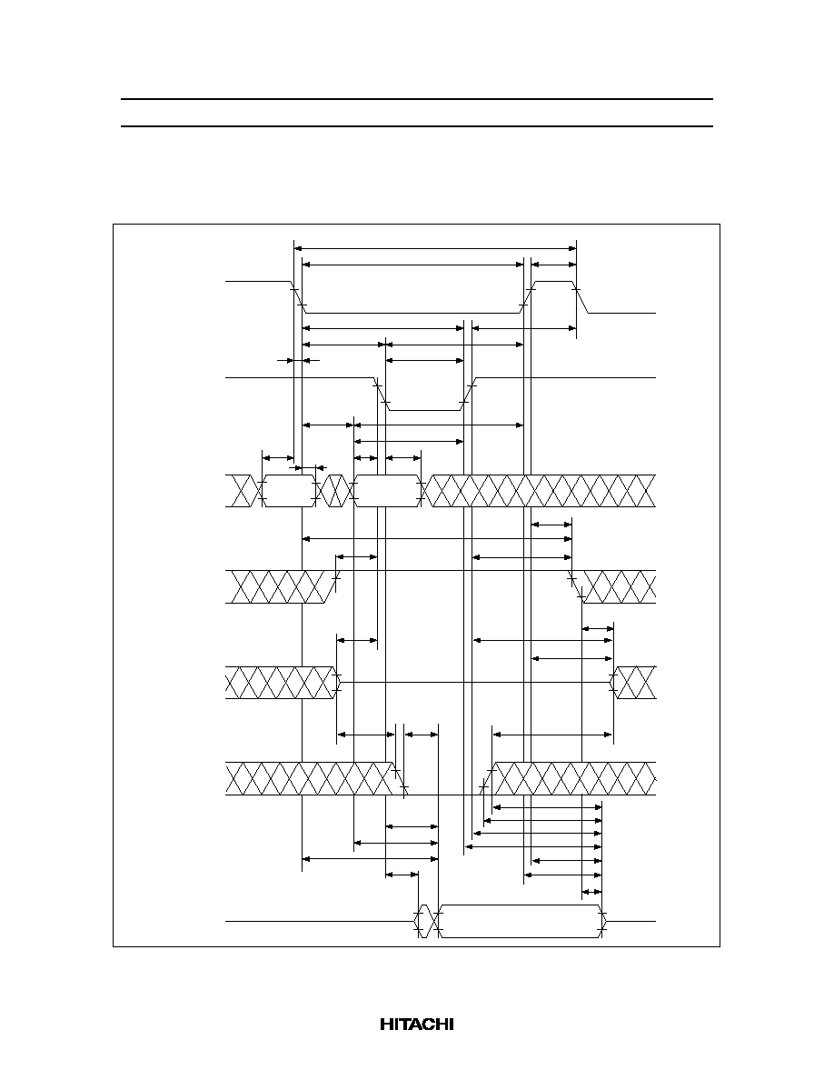
Early Write Cycle
RAS
Address
WE
Din
Dout
t
RC
*
t
RAS
t
RP
t
CRP
t
CSH
t
RCD
t
RSH
t
CAS
t
T
t
ASR
t
RAH
t
ASC
t
CAH
Column
Row
t
WCS
t
WCH
t
DS
t
DH
Din
t
WCS
WCS
(min)
High-Z*
t
CAS
HB56SW3272ESK-5/6
16
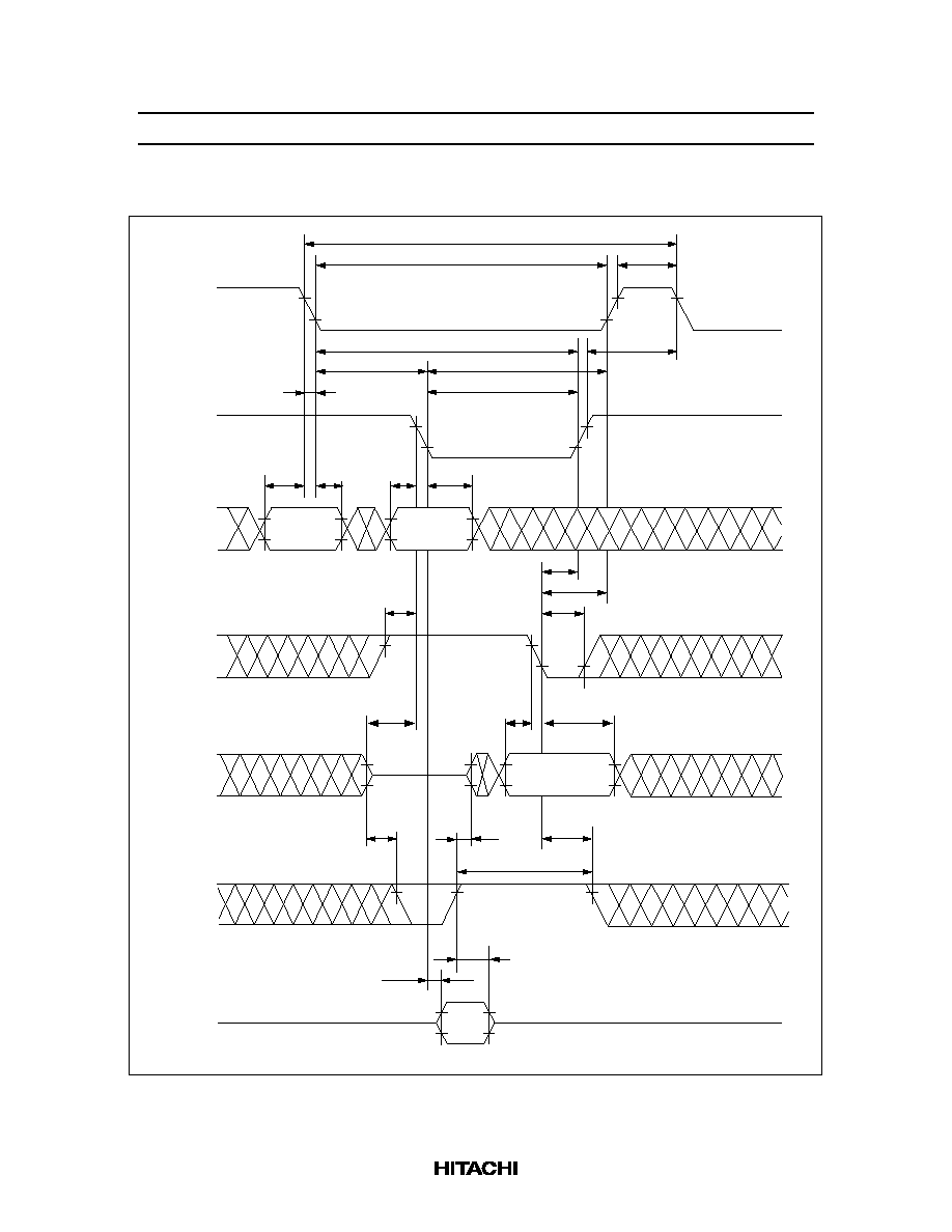
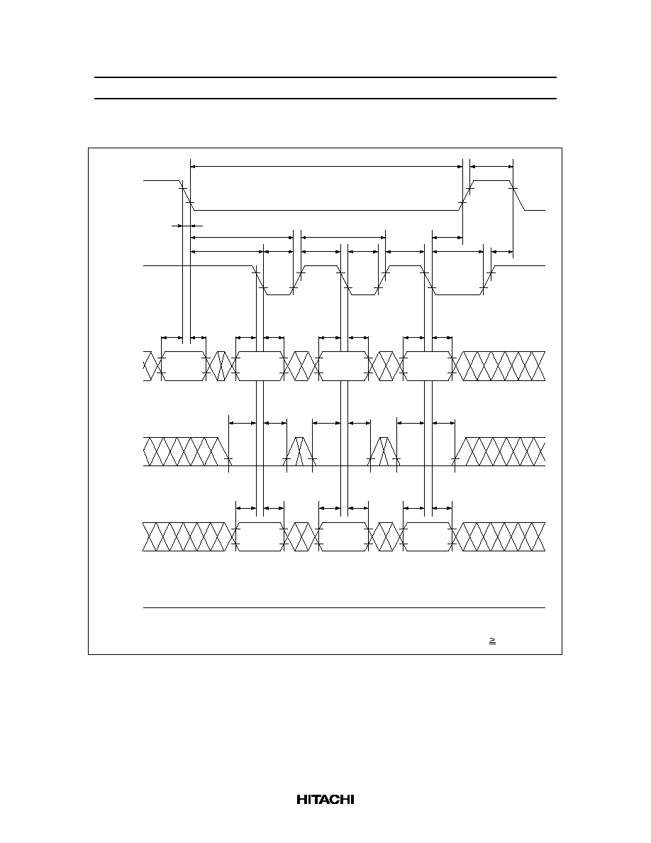
Delayed Write Cycle*
18
Address
CAS
RAS
WE
Din
OE
Dout
t
RC
t
RAS
t
RP
t
CSH
t
RCD
t
RSH
t
CAS
t
CRP
t
T
Column
Row
t
ASR
t
RAH
t
ASC
t
CAH
t
RCS
t
CWL
t
RWL
t
WP
t
DZC
t
DS
t
DH
t
DZO
t
OED
t
OEH
t
OEP
t
CLZ
t
OEZ
High-Z
Invalid Dout
Din
High-Z

HB56SW3272ESK-5/6
17
Read-Modify-Write Cycle*
18
Address
RAS
Din
Dout
OE
WE
t
RWC
t
RAS
t
RP
t
CRP
t
CAS
t
RCD
t
T
t
RAD
t
ASR
t
RAH
t
ASC
t
CAH
Column
Row
t
RCS
t
CWD
t
CWL
t
AWD
t
RWD
t
RWL
t
WP
t
DZC
t
DH
t
DS
Din
High-Z
t
DZO
t
OED
t
OEH
t
OEA
t
CAC
t
AA
t
RAC
t
OHO
t
OEZ
t
CLZ
Dout
High-Z
CAS
t
OEP

HB56SW3272ESK-5/6
18
RAS-Only Refresh Cycle
RAS
CAS
Address
Dout
High-Z
Row
t
RC
t
RP
t
RAS
t
T
t
CRP
t
RPC
t
CRP
t
ASR
t
RAH
t
OFF
t
OFR

HB56SW3272ESK-5/6
19
CAS-Before-RAS Refresh Cycle
RAS
CAS
WE
Address
Dout
High-Z
t
OFF
t
OFR
t
WRP
t
WRH
t
WRP
t
WRH
t
CP
t
RPC
t
CSR
t
CHR
t
CP
t
RPC
t
CSR
t
CHR
t
CRP
t
RP
t
RAS
t
RC
t
RC
t
RP
t
RAS
t
RP
t
T
HB56SW3272ESK-5/6
20
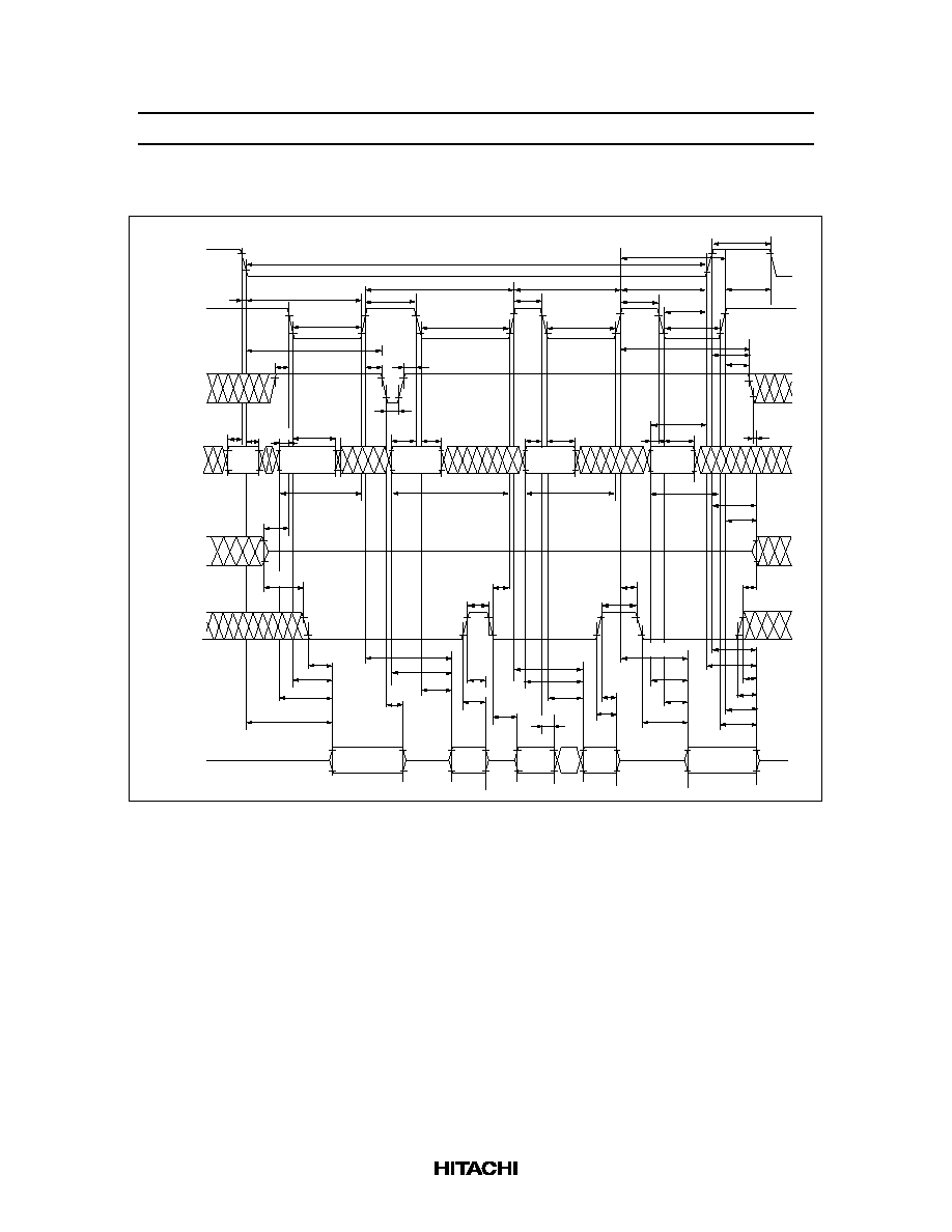
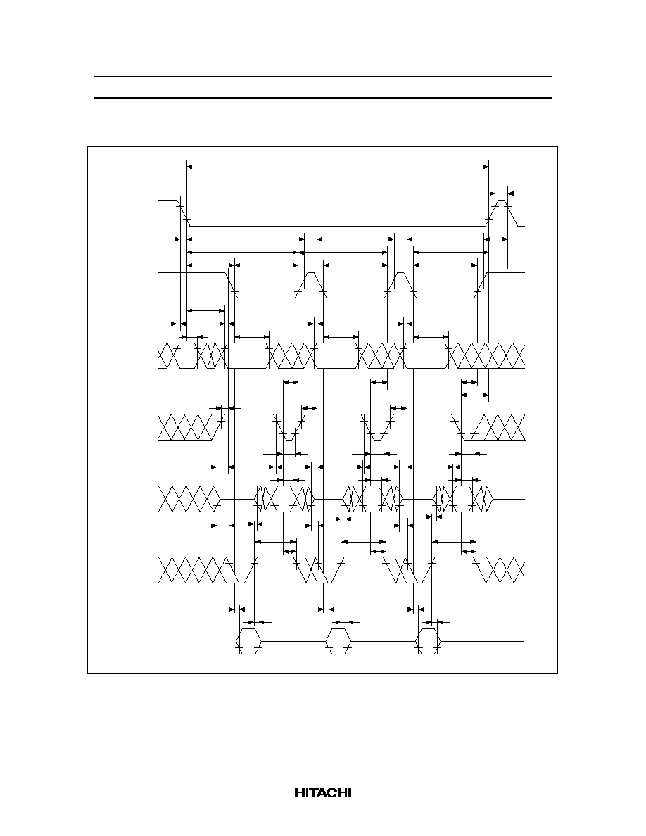
EDO Page Mode Read Cycle (1)
Din
OE
Dout
WE
Address
RAS
CAS
t
CP
t
CP
t
CP
t
T
t
RCH
t
RRH
t
DZC
t
CDD
t
RDD
High-Z
t
OFR
t
OEZ
t
OHO
t
OFF
t
OH
t
OHR
t
t
COL
t
t
CPA
t
AA
t
CAC
t
CAC
t
OEA
t
AA
t
RAC
t
AA
t
CAC
t
CPA
t
t
OEZ
t
OEA
t
OEZ
t
AA
t
CAC
t
t
RASP
COP
t
RP
t
CAS
t
CAS
t
CAS
t
CAL
t
CSH
t
HPC
t
HPC
CRP
t
t
ASR
t
RAH
Column 1
Column 2
Column 3
Column 4
t
t
CAH
t
ASC
t
CAH
t
CAH
t
ASC
t
CAH
t
ASC
t
WED
t
RAL
Row
Dout 2
Dout 2
Dout 4
Dout 1
t
CAS
t
RCS
t
t
RCS
Dout 3
t
OHO
t
t
CPRH
t
HPC
t
OEA
t
WEZ
DZO
t
OED
OHO
DOH
RCH
t
WPE
t
RCHR
t
CAL
t
CAL
t
CAL
t
RSH
t
RCHC
CPA
ASC
t
OEP
t
OEP
HB56SW3272ESK-5/6
21
EDO Page Mode Read Cycle (2)
Din
OE
WE
Address
t
DZC
t
CDD
t
RDD
High-Z
t
OFR
t
OEZ
t
OHO
t
OFF
t
OH
t
OHR
t
t
COL
t
t
CPA
t
AA
t
CAC
t
CAC
t
OEA
t
AA
t
RAC
t
AA
t
DOH
t
t
OEZ
t
t
OEZ
t
AA
t
CAC
t
COP
t
ASR
t
RAH
t
t
CAH
t
ASC
t
CAH
t
CAH
t
ASC
t
CAH
t
ASC
t
WED
t
RAL
Dout 2
Dout 4
Dout 1
t
RCS
t
OHO
t
OEA
DZO
t
OED
t
DOH
t
CAC
t
RCHC
CPA
ASC
RAS
CAS
t
CP
t
CP
t
CP
t
T
t
RCH
t
RRH
t
RASP
t
RP
t
CAS
t
CAS
t
CAS
t
CSH
t
HPC
t
HPC
t
HPC
CRP
t
t
CAS
t
CAL
t
CAL
t
CAL
t
CAL
t
RSH
Dout
Dout 3
Dout 2
OHO
OEA
t
CPA
Column 2
Column 1
Row
Column 3
Column 4
t
OEP
t
OEP
HB56SW3272ESK-5/6
22
EDO Page Mode Early Write Cycle
* t
WCS
WCS
(min)
RAS
Address
WE
Din
Dout
t
RASP
t
RP
t
T
t
CSH
t
HPC
t
RSH
t
CRP
t
CAS
t
CP
t
CAS
t
CP
t
CAS
t
RCD
t
ASR
t
RAH
t
ASC
t
CAH
t
ASC
t
CAH
t
ASC
t
CAH
t
WCH
t
WCS
t
WCH
t
WCS
t
WCH
t
WCS
t
DH
t
DS
t
DH
t
DS
t
DH
t
DS
Din 1
Din 2
Din N
High-Z*
t
Row
Column 1
Column 2
Column N
CAS
HB56SW3272ESK-5/6
23
EDO Page Mode Delayed Write Cycle*
18
WE
Din
OE
Dout
Address
RAS
t
RASP
t
RP
t
CRP
t
RSH
t
CAS
t
HPC
t
CAS
t
CAS
t
CSH
t
RCD
t
T
t
CP
t
CP
t
ASC
t
CAH
t
ASC
t
CAH
t
ASC
t
CAH
t
RAD
t
ASR
t
RAH
t
RCS
t
RCS
t
RCS
t
RWL
t
CWL
t
CWL
t
CWL
t
WP
t
WP
t
WP
t
DZC
t
DS
t
DZC
t
DS
t
DS
t
DZC
t
DH
t
DH
t
DH
t
DZO
t
OED
t
DZO
t
OED
t
DZO
t
OED
t
OEH
t
OEH
t
OEH
t
OEZ
t
CLZ
t
CLZ
t
OEZ
t
CLZ
t
OEZ
Invalid Dout
Invalid Dout
Invalid Dout
Din
1
Din
2
Din
N
Column N
Column 2
Column 1
Row
High-Z
CAS
t
OEP
t
OEP
t
OEP
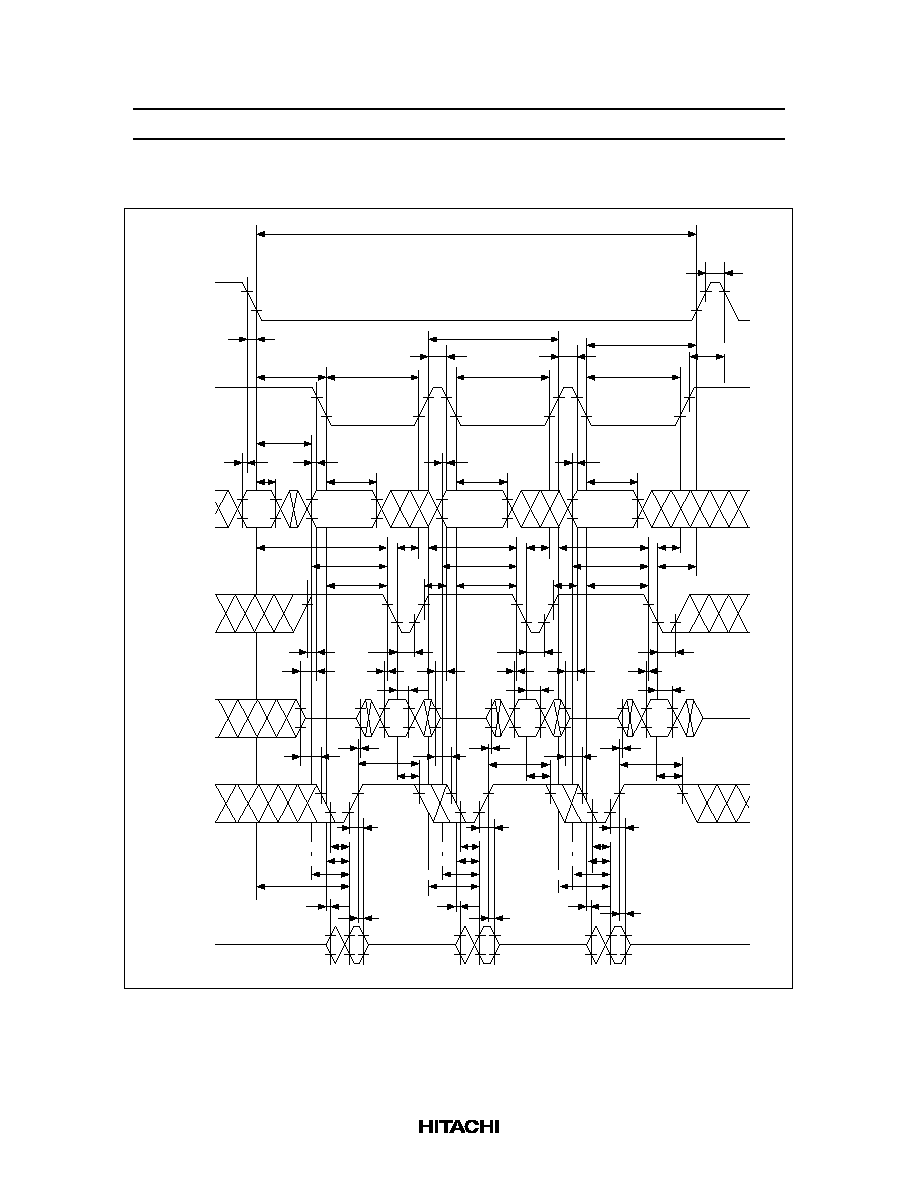
HB56SW3272ESK-5/6
24
EDO Page Mode Read-Modify-Write Cycle*
18
WE
Din
OE
Dout
Address
RAS
t
RASP
t
CRP
t
CP
t
HPRWC
t
T
t
RCD
t
CAS
t
CP
t
CAS
t
CAS
t
RAD
t
ASR
t
ASC
t
ASC
t
ASC
t
RAH
t
CAH
t
CAH
t
CAH
t
CWL
t
CPW
t
CWL
t
CPW
t
CWL
t
RWD
t
AWD
t
AWD
t
AWD
t
CWD
t
RCS
t
CWD
t
RCS
t
CWD
t
RCS
t
WP
t
WP
t
WP
t
DS
t
DZC
t
DS
t
DZC
t
DS
t
DZC
t
DH
t
DH
t
DH
t
DZO
t
DZO
t
DZO
t
OEH
t
OEP
t
OEP
t
OEP
t
OEH
t
OEH
t
AA
t
RAC
t
OEZ
t
CLZ
Dout N
Dout 2
Dout 1
Din
1
Din
2
Din
N
Column N
Column 2
Column 1
t
RP
Row
t
RWL
t
OHO
t
OEA
t
CAC
t
OEZ
t
CLZ
t
OHO
t
OEA
t
CAC
t
CPA
t
OEZ
t
CLZ
t
OHO
t
OEA
t
CAC
t
CPA
High-Z
t
OED
t
OED
t
OED
AA
t
AA
t
t
RSH
CAS
HB56SW3272ESK-5/6
25
EDO Page Mode Mix Cycle (1)*
20
OE
Dout
WE
Address
RAS
CAS
t
CP
t
CP
t
CP
t
T
t
RCH
t
RRH
t
CDD
t
RDD
High-Z
t
OFR
t
OEZ
t
OHO
t
OFF
t
OH
t
CPA
t
AA
t
CAC
t
AA
t
CAC
t
CPA
t
OEZ
t
AA
t
OEA
t
t
RASP
t
RP
t
CAS
t
CAS
t
CAS
CRP
t
t
ASR
t
RAH
Column 1
Column 2
Column 3
Column 4
t
ASC
t
CAH
t
ASC
t
CAH
t
CAH
t
CAH
t
RAL
t
CAL
Row
Dout 2
Dout 4
CPA
t
CAS
t
WCS
Dout 3
t
t
t
WP
t
CWL
t
WCH
t
WED
t
WEZ
t
DS
t
DH
t
DS
t
DH
Din 3
Din 1
t
OEA
t
OED
t
OEP
t
CAC
t
ASC
t
CPW
t
AWD
OHO
t
CAL
t
RCS
t
RCS
t
CSH
t
RCD
t
RSH
DOH
ASC
t
Din

HB56SW3272ESK-5/6
26
EDO Page Mode Mix Cycle (2) *
20
Din
OE
Dout
WE
Address
RAS
CAS
t
CP
t
CP
t
CP
t
T
t
RCH
t
RRH
t
CDD
t
RDD
High-Z
t
OFR
t
OEZ
t
OHO
t
OFF
t
OH
t
CPA
t
AA
t
CAC
t
AA
t
CAC
t
OEZ
t
t
OEA
t
t
RASP
t
RP
t
CAS
t
CAS
t
CAS
t
CSH
CRP
t
t
ASR
t
RAH
Column 1
Column 2
Column 3
Column 4
t
ASC
t
CAH
t
ASC
t
CAH
t
CAH
t
ASC
t
CAH
t
RAL
t
RCS
Row
Dout 1
Dout 4
CPA
t
CAS
t
CWL
Dout 3
t
OHO
t
WED
t
WEZ
t
DS
t
DH
t
DS
t
Din 3
Din 2
t
OEA
t
t
CAC
t
CPW
t
RCH
t
RCS
t
WCH
t
RAC
t
OED
t
COL
t
OEA
t
OHO
t
OEZ
t
DH
OED
t
RCS
t
CAL
t
CAL
t
RCD
t
RCHR
t
WCS
t
RSH
t
WP
t
ASC
AA
t
OEP
t
OEP
COP
HB56SW3272ESK-5/6
27
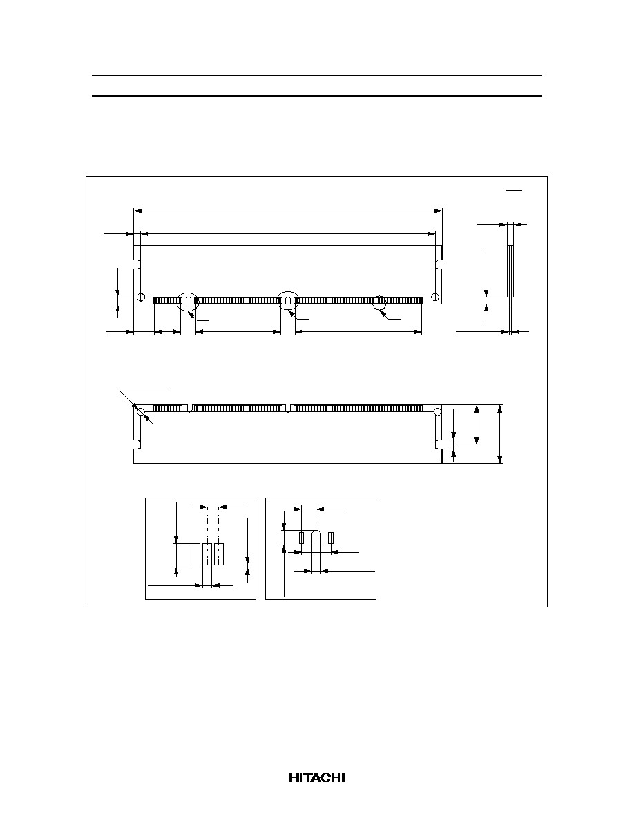
Physical Outline
HB56SW3272ESK Series
3.00
133.35
0.118
5.250
127.35
5.014
3.00
0.118
8.89
11.43
36.83
54.61
0.350
0.450
2.150
1.450
A
B
C
1
84
Front side
Back side
1.27
±
0.10
4.00 min
0.157 min
0.050
±
0.004
4.80
0.189
85
4.00
0.157
17.80
0.701
38.10
1.500
168
2 ≠
3.00
2 ≠
0.118
Component area
(Front)
Component area
(Back)
6.35
0.250
Detail B and C
Detail A
0.20
±
0.15
2.50
±
0.20
0.0079
±
0.0059
0.098
±
0.0079
3.125
±
0.125
0.123
±
0.005
1.27
0.050
1.00
±
0.05
0.039
±
0.002
2.00
±
0.10
0.079
±
0.004
3.175
0.125
Unit: mm
inch
HB56SW3272ESK-5/6
28
Cautions
1. Hitachi neither warrants nor grants licenses of any rights of Hitachi's or any third party's patent,
copyright, trademark, or other intellectual property rights for information contained in this document.
Hitachi bears no responsibility for problems that may arise with third party's rights, including
intellectual property rights, in connection with use of the information contained in this document.
2. Products and product specifications may be subject to change without notice. Confirm that you have
received the latest product standards or specifications before final design, purchase or use.
3. Hitachi makes every attempt to ensure that its products are of high quality and reliability. However,
contact Hitachi's sales office before using the product in an application that demands especially high
quality and reliability or where its failure or malfunction may directly threaten human life or cause risk
of bodily injury, such as aerospace, aeronautics, nuclear power, combustion control, transportation,
traffic, safety equipment or medical equipment for life support.
4. Design your application so that the product is used within the ranges guaranteed by Hitachi particularly
for maximum rating, operating supply voltage range, heat radiation characteristics, installation
conditions and other characteristics. Hitachi bears no responsibility for failure or damage when used
beyond the guaranteed ranges. Even within the guaranteed ranges, consider normally foreseeable
failure rates or failure modes in semiconductor devices and employ systemic measures such as fail-
safes, so that the equipment incorporating Hitachi product does not cause bodily injury, fire or other
consequential damage due to operation of the Hitachi product.
5. This product is not designed to be radiation resistant.
6. No one is permitted to reproduce or duplicate, in any form, the whole or part of this document without
written approval from Hitachi.
7. Contact Hitachi's sales office for any questions regarding this document or Hitachi semiconductor
products.
Hitachi, Ltd.
Semiconductor & IC Div.
Nippon Bldg., 2-6-2, Ohte-machi, Chiyoda-ku, Tokyo 100-0004, Japan
Tel: Tokyo (03) 3270-2111
Fax: (03) 3270-5109
For further information write to:
Hitachi Semiconductor
(America) Inc.
2000 Sierra Point Parkway
Brisbane, CA. 94005-1897
U S A
Tel: 800-285-1601
Fax:303-297-0447
Hitachi Europe GmbH
Continental Europe
Dornacher Straþe 3
D-85622 Feldkirchen
M¸nchen
Tel: 089-9 91 80-0
Fax: 089-9 29 30-00
Hitachi Europe Ltd.
Electronic Components Div.
Northern Europe Headquarters
Whitebrook Park
Lower Cookham Road
Maidenhead
Berkshire SL6 8YA
United Kingdom
Tel: 01628-585000
Fax: 01628-585160
Hitachi Asia Pte. Ltd.
16 Collyer Quay #20-00
Hitachi Tower
Singapore 049318
Tel: 535-2100
Fax: 535-1533
Hitachi Asia (Hong Kong) Ltd.
Unit 706, North Tower,
World Finance Centre,
Harbour City, Canton Road
Tsim Sha Tsui, Kowloon
Hong Kong
Tel: 27359218
Fax: 27306071
Copyright © Hitachi, Ltd., 1998. All rights reserved. Printed in Japan.

HB56SW3272ESK-5/6
29
Revision Record
Rev. Date
Contents of Modification
Drawn by
Approved by
0.0
Jan. 30, 1998 Initial issue
(referred to HM5164405/HM5165405 Series Rev. 0.1)
S. Tsukui
K. Tsuneda
0.1
Mar. 16, 1998 Change of Block Diagram
Change of Physical Outline
S. Tsukui
K. Tsuneda
1.0
Jun. 23, 1998 (referred to HM5164405/HM5165405 Series rev. 1.0)
General Description
Addition of Notes about protection from mechanical
defects
AC Test condition
Addition of Ambient illuminance