HD66740
1
HD66740
(112 x 80-dot Graphics LCD Controller/Driver)
Rev 1.0
August, 2001
Description
The HD66740, 112-by-80 dot-matrix graphics LCD controller and driver LSI, displays graphics such as
text, kanji and pictograms. It can be configured to drive a dot-matrix liquid crystal under the control of the
microprocessor connected via the clock-synchronized serial or 4/8-bit bus. The HD66740 has a smooth
vertical scroll display and a double-height display for the remaining bit map areas. It fixed-displays a part
of the graphics icons so that the user can easily see a variety of information.
The HD66740 has various functions to reduce the power consumption of an LCD system such as low-
voltage operation of 1.8 V min., a booster to generate maximum five-times LCD drive voltage from the
supplied voltage, and voltage-followers to decrease the direct current flow in the LCD drive bleeder-
resistors. Combining these hardware functions with software functions such as standby and sleep modes
allows fine power control. The HD66740 is suitable for any portable battery-driven product requiring
long-term driving capabilities such as cellular phones, pagers, or electronic wallets.
Features
∑
Control and drive of a graphics LCD
∑
112 x 80-dot display
∑
Fixed display of graphics icons (pictograms)
∑
Low-power operation support:
Vcc = 1.8 to 3.6 V (low voltage)
V
LCD
= 4.5 to 15.0 V (liquid crystal drive voltage)
Triple, quadruple, or five-times booster for liquid crystal drive voltage
64-step contrast adjuster and voltage followers to decrease direct current flow in the LCD drive
bleeder-resistors
Power-save functions such as the standby mode and sleep mode supported
Programmable drive duty ratios and bias values displayed on LCD
∑
High-speed clock-synchronized serial interface (serial transfer rate: 5 MHz max.)
∑
I2C bus interface
∑
High-speed 4-/8-bit bus interface capability
∑
112-segment
◊
80-common liquid crystal display driver
∑
1,120-byte (112
◊
80 dots) character generator RAM
HD66740
2
∑
Vertical smooth scroll
∑
Partial smooth scroll control (fixed display of graphics icons)
∑
Vertical double-height display by each display line
∑
Black-and-white reversed display
∑
Wide range of instruction functions:
Display on/off control, black-and-white reversed
∑
No wait time for instruction execution and RAM access
∑
Internal oscillation and hardware reset
∑
n-raster-row AC liquid-crystal drive (C-pattern waveform drive)
∑
Shift change of segment and common driver
∑
Tape carrier package (TCP)
Table 1
Progammable Display Sizes and Duty Ratios
Graphics Display
Duty
Ratio
Optimum
Drive Bias
Bit Map
12 x 13-dot
Font Width
14 x 15-dot
Font Width
16 x 16-dot
Font Width
1/32
1/7
112 x 32 dots 2 lines x 9
characters
2 lines x 8
characters
2 lines x 7
characters
1/40
1/7
112 x 40 dots 3 lines x 9
characters
2.5 lines x 8
characters
2.5 lines x 7
characters
1/48
1/8
112 x 48 dots 3 lines x 9
characters
3 lines x 8
characters
3 line x 7
characters
1/56
1/8
112 x 56 dots 4 lines x 9
characters
3.5 lines x 8
characters
3.5 lines x 7
characters
1/64
1/9
112 x 64 dots 5 lines x 9
characters
4 lines x 8
characters
4 lines x 7
characters
1/72
1/9.5
112 x 72 dots 6 lines x 9
characters
4.5 lines x 8
characters
4.5 lines x 7
characters
1/80
1/10
112 x 80 dots 6 lines x 9
characters
5 lines x 8
characters
5 lines x 7
characters

HD66740
3
<Target values>
Total Current Consumption Characteristics (Vcc = 3 V, TYP Conditions, LCD
Drive Power Current Included)
Total Power Consumption
Normal Display Operation
Character
Display Dot
Size
Duty
Ratio
R-C
Oscillation
Frequency
Frame
Frequency
Internal
Logic
LCD
Power
Total*
Sleep
Mode
Standby
Mode
112 x 32 dots 1/32
75 kHz
73 Hz
(27 µA)
(16 µA)
Triple
(75 µA)
(15 µA) 0.1 µA
112 x 40 dots 1/40
75 kHz
73 Hz
(27 µA)
(16 µA)
Triple
(75 µA)
(15 µA)
112 x 48 dots 1/48
75 kHz
74 Hz
(27 µA)
(16 µA)
Triple
(75 µA)
(15 µA)
112 x 56 dots 1/56
75 kHz
74 Hz
(27 µA)
(16 µA)
Triple
(75 µA)
(15 µA)
112 x 64 dots 1/64
75 kHz
73 Hz
(27 µA)
(18 µA)
Quadruple
(99 µA)
(15 µA)
112 x 72 dots 1/72
80 kHz
70 Hz
(32 µA)
(18 µA)
Quadruple
(104 µA)
(15 µA)
112 x 80 dots 1/80
90 kHz
70 Hz
(35 µA)
(20 µA)
Five-times
(135 µA)
(15 µA)
Note : When a triple, quadruple, or five-times booster is used:
the total power consumption = Internal logic current + LCD power current x 3 (triple booster),
the total power consumption = Internal logic current + LCD power current x 4 (quadruple booster),
and
the total power consumption = Internal logic current + LCD power current x 5 (five-times booster)
Type Name
Types
External
Dimensions
Bus Interface
Operation Voltages
HD66740TB0
Bending TCP
4/8-bits parallel and clock synchronized serial
HD66740WTB0
Bending TCP
4/8-bits parallel and I2C bus interface
HCD66740BP
Au-bumped chip
4/8-bits parallel and clock synchronized serial
HCD66740WBP
Au-bumped chip
4/8-bits parallel and I2C bus interface
1.8 V to 3.6 V

HD66740
4
LCD Specification Comparison
(Under development)
Items
HD66725
HD66728
HD66740
Character display sizes
16 characters x 3 lines
16 characters x 10 lines
--
Graphic display sizes
96 x 26 dots
112 x 80 dots
112 x 80 dots
Multiplexing icons
192
--
--
Annunciator
1/2 duty: 192
--
--
Key scan control
8 x 4
8 x 4
--
LED control ports
--
--
--
General output ports
3
3
--
Operating power voltages
1.8 V to 5.5 V
1.8 V to 5.5 V
1.8 V to 3.6 V
Liquid crystal drive voltages
3 V to 6 V
4.5 V to 15 V
4.5 V to 15 V
I2C bus
--
--
I2C bus interface
(HD66740W)
Serial bus
Clock-synchronized serial
Clock-synchronized serial
Clock-synchronized serial
Parallel bus
4 bits, 8 bits
4 bits, 8 bits
4 bits, 8 bits
Expansion driver control
Impossible
Impossible
Impossible
Liquid crystal drive duty ratios
1/2, 10, 18, 26
1/8, 16, 24, 32, 40, 48, 56, 64
72, 80
1/8, 16, 24, 32, 40, 48, 56, 64
72, 80
Liquid crystal drive biases
1/4 to 1/6.5
1/4 to 1/10
1/4 to 1/10
Liquid crystal drive waveforms
B
B, C
B, C
Liquid crystal voltage booster
Single, double, or triple
Triple, quadruple, or five-
times
Triple, quadruple, or five-
times
Bleeder-resistor for liquid crystal drive
Incorporated (external)
Incorporated (external)
Incorporated (external)
Liquid crystal drive operational amplifier
Incorporated
Incorporated
Incorporated
Liquid crystal contrast adjuster
Incorporated
Incorporated
Incorporated
Horizontal smooth scroll
3-dot unit
--
--
Vertical smooth scroll
Line unit
Line unit
Line unit
Double-height display
Yes
Yes
Yes
DDRAM
80 x 8
160 x 8
--
CGROM
20,736
20,736
--
CGRAM
384 x 8
1,120 x 8
1,120 x 8
SEGRAM
96 x 8
--
--
No. of CGROM fonts
240 + 192
240 + 192
--
No. of CGRAM fonts
64
64
--
Font sizes
6 x 8
6 x 8
--
Bit map areas
96 x 26
112 x 80
112 x 80
R-C oscillation resistor/
oscillation frequency
External resistor,
incorporated (32 kHz)
External resistor
(70≠90 kHz)
External resistor
(70≠90 kHz)
Reset function
External
External
External
Low power control
Partial display off
Oscillation off
Liquid crystal power off
Key wake-up interrupt
Partial display off
Oscillation off
Liquid crystal power off
Key wake-up interrupt
Partial display off
Oscillation off
Liquid crystal power off
SEG/COM direction switching
SEG, COM
SEG, COM
SEG, COM
QFP package
--
--
--
TQFP package
--
--
--
TCP package
TCP-170
TCP-243
TCP-233
Bare chip
--
--
--
Bumped chip
Yes
Yes
Yes
No. of pins
170
243
243
Chip sizes
10.97 x 2.51
13.67 x 2.78
9.40 x 2.18
Pad intervals
80 µm
70 µm
50 µm

HD66740
5
HD66740 Block Diagram
System
interface
- Clock
synchro-
nized
serial
- I2C bus
- 4-bit bus
- 8-bit bus
Data
register
(DR)
Instruction register
(IR)
Address
counter
(AC)
Timing generator
Character
generator RAM
(CGRAM)
1,120 bytes
Parallel/serial converter
112-bit
latch
circuit
112-bit
segment
shift
register
80-bit bidirectional
common shift register
Common
driver
Segment
driver
LCD drive
voltage
selector
CPG
Instruction
decoder
RS
RW/RD*/SDA
E/WR*/SCL
Vcc
V
LCD
COM1/80--
COM80/1
SEG1/112--
SEG112/1
OSC1
OSC2
8
8
8
10
8
Vci
Triple to
five-times
booster
C1+
IM2-1
RESET*
C1-
+ -
+ -
+ -
+ -
VLOUT
+ -
GND
VR
R
R
R
0
R
TEST
V1OUT
V2OUT
V3OUT
V4OUT
V5OUT
OPOFF
IM0/ID
C2+
C2-
CS*
C3+
C3-
Contrast adjuster
Drive bias controller
C4+
C4-
VTEST1--
VTEST3
DB0-DB7

HD66740
6
HD66740 Pad Arrangement
Rev 0.5
- Chip size : 9.40mm x 2.18mm
- Chip thickness : 550um (typ.)
- PAD coordinates : PAD center
- Coodinate origin : Chip center
- Au bump size (pin number is shown in the
blacket)
(1)80um x 80um
Dummy1(1) to Dummy2(78),
Dummy3(104), Dummy20(263)
(2)45um x 80um
COM34(105) to COM80(119)
Dummy4(120)
Dummy5(121) to Dummy10(126)
Dummy13(241) to Dummy18(246)
Dummy19(247)
COM72(248) to COM58(262)
(3)80um x 45um
COM57(264) to COM1(288)
COM9(79) to COM33(103)
(4)35um x 80um
Dummy11(127)
SEG1(128) to SEG112(239)
Dummy12(240)
- Au bump pitch:
Refer PAD coodinate
- Au bump height : 15um(typ.)
- No cross recognition mark
(Top view)
HD66740
OSC2
OSC1
Vci
Y
X
C2-
C2+
C2+
Vci
Vci
Vcc
E/WR*/SCL
VTEST3
VTEST2
VTEST1
GNDDUM2
C1-
C1-
VLOUT
VLOUT
V
LCD
V
LCD
C1+
Vcc
Vcc
RW/RD*/SDA
GND
GND
GND
RS
CS*
RESET*
DB0
DB1
DB2
DB3
DB4
DB5
DB6
DB7
GNDDUM
IM2
IM1
IM0/ID
VccDUM
OPOFF
TEST
C3-
C3-
C3+
C3+
V1OUT
V2OUT
V3OUT
V4OUT
V5OUT
COM1/80
COM2/79
COM3/78
COM4/77
COM6/75
COM7/74
COM8/73
COM41/40
COM42/39
COM43/38
COM44/37
COM5/76
COM45/36
COM46/35
COM47/34
COM48/33
COM49/32
COM50/31
COM51/30
COM52/29
COM53/28
COM54/27
COM55/26
COM56/25
COM14/67
COM15/66
COM16/65
COM17/64
COM18/63
COM19/62
COM21/60
COM22/59
COM23/58
COM24/57
COM25/56
COM26/55
COM27/54
COM28/53
COM20/61
COM29/52
COM30/51
COM13/68
COM12/69
COM11/70
COM10/71
COM31/50
COM32/49
SEG9/104
SEG8/105
SEG7/106
SEG6/107
SEG5/108
SEG4/109
SEG101/12
SEG102/11
SEG103/10
SEG104/9
SEG105/8
SEG106/7
SEG107/6
SEG108/5
SEG109/4
SEG112/1
SEG111/2
SEG1/112
SEG2/111
SEG3/110
SEG110/3
COM57/24
COM33/48
SEG10/103
SEG11/102
SEG100/13
SEG99/14
SEG12/101
SEG13/100
SEG14/99
C4-
C4-
C4+
C4+
COM72/9
COM71/10
COM70/11
COM69/12
COM68/13
COM67/14
COM66/15
COM58/23
COM59/22
COM60/21
COM61/20
COM62/19
COM63/18
COM64/17
COM65/16
COM80/1
COM79/2
COM78/3
COM77/4
COM76/5
COM75/6
COM74/7
COM34/47
COM35/46
COM36/45
COM37/44
COM38/43
COM39/42
COM40/41
COM73/8
Dummy1
SEG25/88
SEG26/87
SEG27/86
SEG28/85
SEG29/84
SEG30/83
SEG31/82
SEG32/81
SEG33/80
SEG34/79
SEG35/78
SEG36/77
SEG37/76
SEG38/75
SEG39/74
SEG40/73
SEG41/72
SEG42/71
SEG43/70
SEG44/69
SEG45/68
SEG46/67
SEG47/66
SEG48/65
SEG49/64
SEG50/63
SEG51/62
SEG52/61
SEG53/60
SEG54/59
SEG55/58
SEG56/57
SEG57/56
SEG58/55
SEG59/54
SEG60/53
SEG61/52
SEG62/51
SEG63/50
SEG64/49
SEG65/48
SEG66/47
SEG67/46
SEG68/45
SEG69/44
SEG70/43
SEG71/42
SEG72/41
SEG73/40
SEG74/39
SEG75/38
SEG76/37
SEG77/36
SEG78/35
SEG79/34
SEG80/33
SEG81/32
SEG82/31
SEG83/30
SEG84/29
SEG85/28
SEG86/27
SEG87/26
SEG88/25
SEG89/24
SEG90/23
SEG91/22
SEG92/21
SEG93/20
SEG94/19
SEG95/18
SEG96/17
SEG97/16
SEG98/15
SEG24/89
SEG23/90
SEG22/91
SEG21/92
SEG20/93
SEG19/94
SEG18/95
SEG17/96
SEG16/97
SEG15/98
COM9/72
C1+
C2-
VLOUT
V
LCD
Dummy2
Dummy3
Dummy4
Dummy5
Dummy6
Dummy7
Dummy11
Dummy20
Vcc
GND
C3+
C4-
C4+
C2-
C2+
C1-
VLOUT
V
LCD
C1+
C3-
Dummy8
Dummy9
Dummy12
Dummy13
Dummy14
Dummy15
Dummy19
Dummy16
Dummy17
Vci
Dummy10
Dummy18
GND
HD66740
TYPE CODE
NO.1
NO.2
NO.288
NO.78
NO.77
NO.79
NO.103
NO.104
NO.105
NO.262
NO.263
NO.264

HD66740
7
HD66740 Pad Coordinate
2000.06.13 (Unit : um)
No.
PAD NAME
X
Y
No.
PAD NAME
X
Y
No.
PAD NAME
X
Y
No.
PAD NAME
X
Y
1
DUMMY1
-4538
-930
73
V5OUT
3834
-930
145
SEG18/95
1930
928
217
SEG90/23
-1679
928
2
GNDDUM
-4336
-930
74
VTEST1
3936
-930
146
SEG19/94
1880
928
218
SEG91/22
-1729
928
3
IM2
-4190
-930
75
VTEST2
4038
-930
147
SEG20/93
1829
928
219
SEG92/21
-1779
928
4
IM1
-4045
-930
76
VTEST3
4140
-930
148
SEG21/92
1779
928
220
SEG93/20
-1829
928
5
IM0/ID
-3915
-930
77
GNDDUM2
4336
-930
149
SEG22/91
1729
928
221
SEG94/19
-1880
928
6
VCCDUM
-3813
-930
78
DUMMY2
4538
-930
150
SEG23/90
1679
928
222
SEG95/18
-1930
928
7
OPOFF
-3711
-930
79
COM9/72
4538
-721
151
SEG24/89
1629
928
223
SEG96/17
-1980
928
8
TEST
-3609
-930
80
COM10/71
4538
-661
152
SEG25/88
1579
928
224
SEG97/16
-2030
928
9
DB7
-3466
-930
81
COM11/70
4538
-601
153
SEG26/87
1529
928
225
SEG98/15
-2080
928
10
DB6
-3321
-930
82
COM12/69
4538
-541
154
SEG27/86
1479
928
226
SEG99/14
-2130
928
11
DB5
-3177
-930
83
COM13/68
4538
-481
155
SEG28/85
1428
928
227
SEG100/13
-2180
928
12
DB4
-3032
-930
84
COM14/67
4538
-421
156
SEG29/84
1378
928
228
SEG101/12
-2230
928
13
DB3
-2887
-930
85
COM15/66
4538
-361
157
SEG30/83
1328
928
229
SEG102/11
-2281
928
14
DB2
-2742
-930
86
COM16/65
4538
-301
158
SEG31/82
1278
928
230
SEG103/10
-2331
928
15
DB1
-2597
-930
87
COM17/64
4538
-240
159
SEG32/81
1228
928
231
SEG104/9
-2381
928
16
DB0
-2453
-930
88
COM18/63
4538
-180
160
SEG33/80
1178
928
232
SEG105/8
-2431
928
17
RESET*
-2308
-930
89
COM19/62
4538
-120
161
SEG34/79
1128
928
233
SEG106/7
-2481
928
18
CS*
-2163
-930
90
COM20/61
4538
-60
162
SEG35/78
1078
928
234
SEG107/6
-2531
928
19
RS
-2018
-930
91
COM21/60
4538
0
163
SEG36/77
1028
928
235
SEG108/5
-2581
928
20
E/WR*/SCL
-1873
-930
92
COM22/59
4538
60
164
SEG37/76
977
928
236
SEG109/4
-2631
928
21
RW/RD*/SDA
-1729
-930
93
COM23/58
4538
120
165
SEG38/75
927
928
237
SEG110/3
-2682
928
22
GND
-1627
-930
94
COM24/57
4538
180
166
SEG39/74
877
928
238
SEG111/2
-2732
928
23
GND
-1525
-930
95
COM25/56
4538
240
167
SEG40/73
827
928
239
SEG112/1
-2782
928
24
GND
-1423
-930
96
COM26/55
4538
301
168
SEG41/72
777
928
240
DUMMY12
-2836
928
25
GND
-1321
-930
97
COM27/54
4538
361
169
SEG42/71
727
928
241
DUMMY13
-2981
928
26
GND
-1219
-930
98
COM28/53
4538
421
170
SEG43/70
677
928
242
DUMMY14
-3041
928
27
OSC2
-1117
-930
99
COM29/52
4538
481
171
SEG44/69
627
928
243
DUMMY15
-3101
928
28
OSC1
-972
-930
100
COM30/51
4538
541
172
SEG45/68
576
928
244
DUMMY16
-3161
928
29
VCC
-791
-930
101
COM31/50
4538
601
173
SEG46/67
526
928
245
DUMMY17
-3221
928
30
VCC
-689
-930
102
COM32/49
4538
661
174
SEG47/66
476
928
246
DUMMY18
-3281
928
31
VCC
-587
-930
103
COM33/48
4538
721
175
SEG48/65
426
928
247
DUMMY19
-3431
928
32
VCC
-485
-930
104
DUMMY3
4538
928
176
SEG49/64
376
928
248
COM72/9
-3495
928
33
VCI
-332
-930
105
COM34/47
4336
928
177
SEG50/63
326
928
249
COM71/10
-3555
928
34
VCI
-230
-930
106
COM35/46
4276
928
178
SEG51/62
276
928
250
COM70/11
-3615
928
35
VCI
-128
-930
107
COM36/45
4216
928
179
SEG52/61
226
928
251
COM69/12
-3675
928
36
VCI
-26
-930
108
COM37/44
4156
928
180
SEG53/60
175
928
252
COM68/13
-3735
928
37
C4+
76
-930
109
COM38/43
4096
928
181
SEG54/59
125
928
253
COM67/14
-3795
928
38
C4+
178
-930
110
COM39/42
4036
928
182
SEG55/58
75
928
254
COM66/15
-3856
928
39
C4+
280
-930
111
COM40/41
3976
928
183
SEG56/57
25
928
255
COM65/16
-3916
928
40
C4-
381
-930
112
COM73/8
3916
928
184
SEG57/56
-25
928
256
COM64/17
-3976
928
41
C4-
483
-930
113
COM74/7
3856
928
185
SEG58/55
-75
928
257
COM63/18
-4036
928
42
C4-
585
-930
114
COM75/6
3795
928
186
SEG59/54
-125
928
258
COM62/19
-4096
928
43
C3+
687
-930
115
COM76/5
3735
928
187
SEG60/53
-175
928
259
COM61/20
-4156
928
44
C3+
789
-930
116
COM77/4
3675
928
188
SEG61/52
-226
928
260
COM60/21
-4216
928
45
C3+
891
-930
117
COM78/3
3615
928
189
SEG62/51
-276
928
261
COM59/22
-4276
928
46
C3-
993
-930
118
COM79/2
3555
928
190
SEG63/50
-326
928
262
COM58/23
-4336
928
47
C3-
1095
-930
119
COM80/1
3495
928
191
SEG64/49
-376
928
263
DUMMY20
-4538
928
48
C3-
1197
-930
120
DUMMY4
3431
928
192
SEG65/48
-426
928
264
COM57/24
-4538
721
49
C2+
1299
-930
121
DUMMY5
3281
928
193
SEG66/47
-476
928
265
COM56/25
-4538
661
50
C2+
1401
-930
122
DUMMY6
3221
928
194
SEG67/46
-526
928
266
COM55/26
-4538
601
51
C2+
1503
-930
123
DUMMY7
3161
928
195
SEG68/45
-576
928
267
COM54/27
-4538
541
52
C2-
1605
-930
124
DUMMY8
3101
928
196
SEG69/44
-627
928
268
COM53/28
-4538
481
53
C2-
1707
-930
125
DUMMY9
3041
928
197
SEG70/43
-677
928
269
COM52/29
-4538
421
54
C2-
1809
-930
126
DUMMY10
2981
928
198
SEG71/42
-727
928
270
COM51/30
-4538
361
55
C1+
1911
-930
127
DUMMY11
2836
928
199
SEG72/41
-777
928
271
COM50/31
-4538
301
56
C1+
2013
-930
128
SEG1/112
2782
928
200
SEG73/40
-827
928
272
COM49/32
-4538
240
57
C1+
2115
-930
129
SEG2/111
2732
928
201
SEG74/39
-877
928
273
COM48/33
-4538
180
58
C1-
2217
-930
130
SEG3/110
2682
928
202
SEG75/38
-927
928
274
COM47/34
-4538
120
59
C1-
2319
-930
131
SEG4/109
2631
928
203
SEG76/37
-977
928
275
COM46/35
-4538
60
60
C1-
2421
-930
132
SEG5/108
2581
928
204
SEG77/36
-1028
928
276
COM45/36
-4538
0
61
VLOUT
2523
-930
133
SEG6/107
2531
928
205
SEG78/35
-1078
928
277
COM44/37
-4538
-60
62
VLOUT
2625
-930
134
SEG7/106
2481
928
206
SEG79/34
-1128
928
278
COM43/38
-4538
-120
63
VLOUT
2727
-930
135
SEG8/105
2431
928
207
SEG80/33
-1178
928
279
COM42/39
-4538
-180
64
VLOUT
2829
-930
136
SEG9/104
2381
928
208
SEG81/32
-1228
928
280
COM41/40
-4538
-240
65
VLCD
2930
-930
137
SEG10/103
2331
928
209
SEG82/31
-1278
928
281
COM8/73
-4538
-301
66
VLCD
3032
-930
138
SEG11/102
2281
928
210
SEG83/30
-1328
928
282
COM7/74
-4538
-361
67
VLCD
3134
-930
139
SEG12/101
2230
928
211
SEG84/29
-1378
928
283
COM6/75
-4538
-421
68
VLCD
3236
-930
140
SEG13/100
2180
928
212
SEG85/28
-1428
928
284
COM5/76
-4538
-481
69
V1OUT
3426
-930
141
SEG14/99
2130
928
213
SEG86/27
-1479
928
285
COM4/77
-4538
-541
70
V2OUT
3528
-930
142
SEG15/98
2080
928
214
SEG87/26
-1529
928
286
COM3/78
-4538
-601
71
V3OUT
3630
-930
143
SEG16/97
2030
928
215
SEG88/25
-1579
928
287
COM2/79
-4538
-661
72
V4OUT
3732
-930
144
SEG17/96
1980
928
216
SEG89/24
-1629
928
288
COM1/80
-4538
-721

HD66740
8
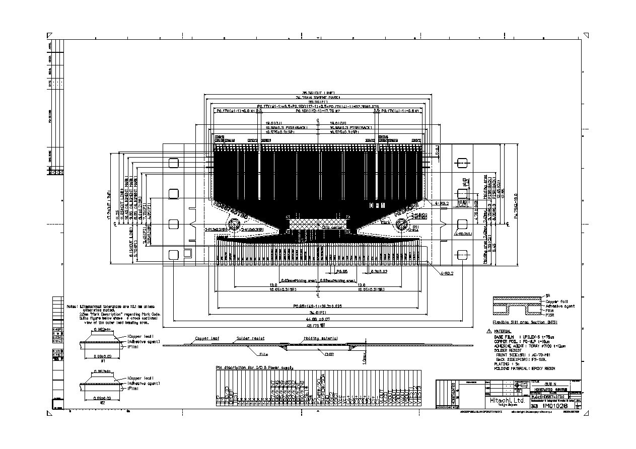
TCP Dimensions (HD66740TB0)
COM1/80
COM8/73
SEG112/1
SEG1/112
COM9/72
0.16-mm
pitch
HITACHI
HITACHI
HD66740
HD66740
COM41/40
COM72/9
IM2
IM1
IM0/ID
OPOFF
TEST
NC
NC
NC
NC
NC
DB7
DB6
DB5
DB4
DB3
DB2
DB1
DB0
RESET*
CS*
RS
E/WR*/SCL
RW/RD*/SDA
GND
OSC2
OSC1
Vcc
Vci
C2+
C2-
C1+
C1-
VLOUT
VLCD
V1OUT
V2OUT
V3OUT
V4OUT
V5OUT
NC
NC
NC
VTEST1
VTSET2
VTEST3
0.65-mm
pitch
Dummy
Dummy
C3+
C3-
COM80/1
COM73/8
COM40/41
Bending slit
4.0 mm
0.17P x (41 ≠ 1)
= 6.80 mm
0.17P x (41 ≠ 1)
= 6.80 mm
0.50 mm
0.50 mm
32.36 mm
SEG111/2
SEG110/3
SEG109/4
SEG2/111
SEG3/110
SEG4/109
C4+
C4-
I/O, Power supply
0.65P x (49 ≠ 1)
= 31.20 mm
LCD drive
0.16P x (112 ≠ 1)
= 17.76 mm
HD66740
9
Pin Functions
Table 2
Pin Functional Description
Signals
Number of
Pins
I/O
Connected to
Functions
IM2, IM1
2
I
GND or V
CC
Selects the MPU interface mode:
IM2
"GND"
"GND"
"Vcc"
"Vcc"
IM1
"GND"
"Vcc"
"GND"
"Vcc"
MPU interface mode
Clock synchronized serial interface
68-system parallel interface
I2C bus interface
80-system parallel interface
IM0/ID
1
I
GND or V
CC
Selects the transfer bus length for a parallel bus
interface.
GND: 8-bit bus, Vcc: 4-bit bus
Inputs the ID of the device ID code for a serial bus and
I2C bus interface.
CS*
1
I
MPU
Selects the HD66740:
Low: HD66740 is selected and can be accessed
High: HD66740 is not selected and cannot be
accessed
Must be fixed at GND level when not in use.
RS
1
I
MPU
Selects the register for a parallel bus interface.
Low: Instruction
High: RAM access
Must be fixed at GND level when not in use.
E/WR*/SCL
1
I
MPU
For an 80-system parallel bus interface, serves as a
write strobe signal and writes data at the low level.
For a 68-system parallel bus interface, serves as an
enable signal to activate data read/write operation.
Inputs the serial transfer clock for a serial interface.
Fetches data at the rising edge of a clock.
RW/RD*/
SDA
1
I or
I/O
MPU
For an 80-system parallel bus interface, serves as a
write strobe signal and reads data at the low level.
For a 68-system parallel bus interface, serves as a
signal to select data read/write operation.
Low: Write High: Read
Serves as the bidirectional serial transfer data for a
serial interface. Sends/Receives data.

HD66740
10
Table 2
Pin Functional Description (cont)
Signals
Number of
Pins
I/O
Connected to
Functions
DB0≠DB7
8
I/O or
I
MPU
Serves as a bidirectional data bus for a parallel bus
interface.
For a 4-bit bus, data transfer uses DB7-DB4
Must be fixed at GND level when serial interface mode
is used.
COM1/80≠
COM80/1
80
O
LCD
Common output signals for graphics display: COM1 to
COM8 for the first line, COM9 to COM16 for the
second line, COM17 to COM24 for the third line,
COM25 to COM32 for the fourth line, and COM73 to
COM80 for the 10th line. All the unused pins output
unselected waveforms. In the sleep mode (SLP = 1) or
standby mode (STB = 1), all pins output GND level.
The CMS bit can change the shift direction of the
common signal. For example, if CMS = 0, COM1/80 is
COM1. If CMS = 1, COM1/80 is COM80.
Note that the start position of the common output (the
first line) is shifted by CN1≠CN0 bits.
SEG1/112≠
SEG112/1
112
O
LCD
Segment output signals for graphics display. In the
sleep mode (SLP = 1) or standby mode (STB = 1), all
pins output GND level.
The SGS bit can change the shift direction of the
segment signal. For example, if SGS = 0, SEG1/112 is
SEG1. If SGS = 1, SEG1/112 is SEG112.
V1OUT≠V5
OUT
5
I or O
Open or
external
bleeder-resistor
Used for output from the internal operational amplifiers
when they are used (OPOFF = GND); attach a
capacitor to stabilize the output. When the amplifiers
are not used (OPOFF = V
CC
), V1 to V5 voltages can be
supplied to these pins externally.
V
LCD
3
--
Power supply
Power supply for LCD drive. V
LCD
≠ GND = 15 V max.
V
CC
, GND
12
--
Power supply
V
CC
: +1.8 V to +3.6 V; GND (logic): 0 V
OSC1,
OSC2
2
I or O
Oscillation-
resistor or clock
For R-C oscillation using an external resistor, connect
an external resistor. For external clock supply, input
clock pulses to OSC1.
Vci
5
I
Power supply
Inputs a reference voltage and supplies power to the
booster; generates the liquid crystal display drive
voltage from the operating voltage. The boosting
output voltage must not be larger than the absolute
maximum ratings.
Must be left disconnected when the booster is not
used.
VLOUT
3
O
V
LCD
pin/booster
capacitance
Potential difference between Vci and GND is triple- to
five-times-boosted and then output. Magnitude of
boost is selected by instruction.

HD66740
11
Table 2
Pin Functional Description (cont)
Signals
Number of
Pins
I/O
Connected to
Functions
C1+, C1≠
8
--
Booster
capacitance
External capacitance should be connected here for
boosting.
C2+, C2≠
6
--
Booster
capacitance
External capacitance should be connected here when
using the triple or more booster.
C3+, C3≠
6
--
Booster
capacitance
External capacitance should be connected here when
using the quadruple and five-times booster.
C4+, C4≠
6
--
Booster
capacitance
External capacitance should be connected here when
using the five-times booster.
RESET*
1
I
MPU or external
R-C circuit
Reset pin. Initializes the LSI when low.
OPOFF
1
I
V
CC
or GND
Turns the internal operational amplifier off when
OPOFF = V
CC
, and turns it on when OPOFF = GND. If
the amplifier is turned off (OPOFF = V
CC
), V1 to V5
must be supplied to the V1OUT to V5OUT pins.
VccDUM
1
O
Input pins
Outputs the internal V
CC
level; shorting this pin sets the
adjacent input pin to the V
CC
level.
GNDDUM
1
O
Input pins
Outputs the internal GND level; shorting this pin sets
the adjacent input pin to the GND level.
Dummy
5
--
--
Dummy pad. Must be left disconnected.
TEST
1
I
GND
Test pin. Must be fixed at GND level.
VTEST1
1
I
GND or V
CC
Adjusts the driving capability of the internal operationa
amplifier for the LCD. This signal enters the normal
drive mode in the GND side, and it enters the high-
power drive mode in the V
CC
side. When the display
quality is not sufficient, use the high-power drive mode
even though the power-consumption current is large.
VTEST2
1
--
--
Test pin. Must be left disconnected.
VTEST3
1
I
V
CC
or GND
Adjusts the driving capability of the internal operationa
amplifier for the LCD. This signal enters the normal
drive mode or high-power mode in the GND side
according to the VTEST1 pin setting, and it enters the
low-power drive mode in the V
CC
side. Use this signa
in the low-power mode so that the display quality is no
lowered.

HD66740
12
Block Function Description
System Interface
The HD66740 has six types of system interfaces, and a clock-synchronized serial, an I2C bus interface, a
68-system 4-bit/8-bit bus, and a 80-system 4-bit/8-bit bus. The interface mode is selected by the IM2-0
pins.
The HD66740 has two 8-bit registers: an instruction register (IR) and a data register (DR).
The IR stores instruction codes, such as clear display, display control, and address information for the
display character generator RAM (CGRAM).
The DR temporarily stores data to be written into the CGRAM. Data written into the DR from the MPU is
automatically written into the CGRAM by internal operation. When address information is written into the
IR, data is read and then stored in the DR from the CGRAM by internal operation. Data is read through the
DR when reading from the RAM, and the first read data is invalid and the second and the following data are
normal. After reading, data in the CGRAM at the next address is sent to the DR for the next reading from
the MPU.
Execution time for instruction excluding clear display is 0 clock cycle and instructions can be written in
succession.
Table 3
Register Selection by RS and R/W Bits
R/W Bit
RS Bit
Operations
0
0
Write instructions to IR
1
0
-
0
1
DR write as an internal operation (DR to CGRAM)
1
1
DR read as an internal operation (CGRAM to DR)
Address Counter (AC)
The address counter (AC) assigns addresses to the CGRAM. When an address set instruction is written into
the IR, the address information is sent from the IR to the AC.
After writing into the CGRAM, the AC is automatically incremented by 1 (or decremented by 1). After
reading from the data, the RDM bit automatically updates or does not update the AC.
Character Generator RAM (CGRAM)
The CGRAM serves as a RAM to store 112 x 80-dot bit pattern data in the graphics display mode. Here,
display patterns are directly written into CGRAM. For details, see the Graphics Display section.
Timing Generator
The timing generator generates timing signals for the operation of internal circuits such as the CGRAM.
The RAM read timing for display and internal operation timing by MPU access are generated separately to
avoid interference with one another. This prevents flickering in areas other than the display area when
writing data to the CGRAM, for example.

HD66740
13
Oscillation Circuit (OSC)
The HD66740 can provide R-C oscillation simply through the addition of an external oscillation-resistor
between the OSC1 and OSC2 pins. The appropriate oscillation frequency for operating voltage, display size,
and frame frequency can be obtained by adjusting the external-resistor value. Clock pulses can also be
supplied externally. Since R-C oscillation stops during the standby mode, current consumption can be
reduced. For details, see the Oscillation circuit section.
Liquid Crystal Display Driver Circuit
The liquid crystal display driver circuit consists of 80 common signal drivers (COM1 to COM80) and 112
segment signal drivers (SEG1 to SEG112). When the number of lines are selected by a program, the
required common signal drivers automatically output drive waveforms, while the other common signal
drivers continue to output unselected waveforms.
Graphics data is sent serially through a 112-bit shift register and latched when all needed data has arrived.
The latched data then enables the segment signal drivers to generate drive waveform outputs.
The shift direction of 112-bit data can be changed by the SGS bit. The shift direction for the common driver
can also be changed by the CMS bit by selecting an appropriate direction for the device mounting
configuration.
When display is off, or during the standby or sleep mode, all the above common and segment signal drivers
output the GND level, halting the display.
Booster (DC-DC Converter)
The booster generates triple, quadruple, or five-times voltage input to the Vci pin. With this, both the
internal logic units and LCD drivers can be controlled with a single power supply. Boost output level from
triple to five-times boost can be selected by software. For details, see the Power Supply for Liquid Crystal
Display Drive section.
V-Pin Voltage Follower
A voltage follower for each voltage level (V1 to V5) reduces current consumption by the LCD drive power
supply circuit. No external resistors are required because of the internal bleeder-resistor, which generates
different levels of LCD drive voltage. This internal bleeder-resistor can be software-specified from 1/4 bias
to 1/10 bias, according to the liquid crystal display drive duty value. The voltage followers can be turned off
while multiplexing drive is not being used. For details, see the Power Supply for Liquid Crystal Display
Drive section.
Contrast Adjuster
The contrast adjuster can be used to adjust LCD contrast in 64 steps by varying the LCD drive voltage by
software. This can be used to select an appropriate LCD brightness or to compensate for temperature.

HD66740
14
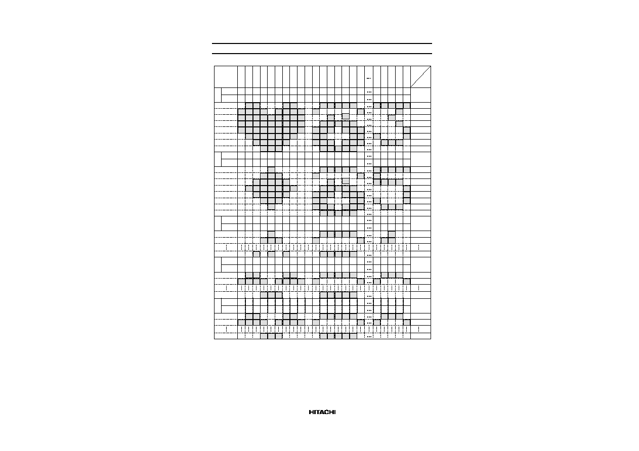
CGRAM Address Map
Table 4
Relationship between Display Position and CGRAM Address (1)
DB0
000
DB1
DB2
DB3
DB4
DB5
DB6
DB7
001 002 003 004 005 006 007 008 009 00A 00B 00C 00D 00E 00F 010
06E 06F
06D
06C
06B
COM1
COM2
COM3
COM4
COM5
COM6
COM7
COM8
DB0
080
DB1
DB2
DB3
DB4
DB5
DB6
DB7
081 082 083 084 085 086 087 088 089 08A 08B 08C 08D 08E 08F 090
0EE 0EF
0ED
0EC
0EB
COM9
COM10
COM11
COM12
COM13
COM14
COM15
COM16
DB0
100
DB1
DB7
101 102 103 104 105 106 107 108 109 10A 10B 10C 10D10E 10F 110
16E 16F
16D
16C
16B
COM17
COM18
COM24
SEG1/112
SEG2/111
SEG3/110
SEG4/109
SEG5/108
SEG6/107
SEG7/106
SEG8/105
SEG9/104
SEG10/103
SEG11/102
SEG12/101
SEG13/100
SEG14/99
SEG15/98
SEG16/97
SEG17/96
SEG108/5
SEG109/4
SEG110/3
SEG111/2
SEG112/1
1
1
1
1
1
1
1
1
1
1
1
1
1
1
1
1
1
1
1
1
1
1
1
1
1
1
1
1
1
1
1
1
1
1
1
1
1
1
1
1
1
1
1
1
1
1
1
1
1
1
1
1
1
1
1
1
1
1
1
1
1
1
1
1
1
1
1
1
1
1
1
1
1
1
1
1
1
1
1
1
1
1
1
1
1
1
1
1
1
1
1
0
0
0
0
0
0
0
0
0
0
0
0
0
0
0
0
0
0
0
0
0
0
0
0
0
0
0
0
0
0
0
0
0
0
0
0
0
0
0
0
0
0
0
0
0
0
0
0
0
0
0
0
0
0
0
0
0
0
0
0
0
0
0
0
0
0
0
0
0
0
0
0
0
0
0
0
0
0
0
0
0
0
0
0
0
0
0
0
0
0
0
0
0
0
0
0
0
0
0
0
0
0
0
0
0
0
0
0
0
0
0
0
0
0
0
0
0
0
0
0
0
0
0
0
0
0
0
0
0
0
0
0
0
0
0
0
0
0
0
0
0
0
0
0
0
0
0
0
0
0
0
0
0
0
0
0
0
0
0
0
0
0
(HEX)
(HEX)
(HEX)
0
0
0
0
0
0
0
0
0
0
0
0
0
0
0
0
0
0
0
DB0
180
DB1
DB7
181 182 183 184 185 186 187 188 189 18A 18B 18C 18D 18E 18F 180
1EE 1EF
1ED
1EC
1EB
COM25
COM26
COM32
0
0
0
1
0
1
1
0
1
1
1
0
0
0
0
0
0
0
0
0
0
0
0
0
0
0
0
0
0
0
0
0
0
0
0
0
0
0
0
0
0
0
1
0
0
0
0
0
(HEX)
0
0
0
0
0
0
0
0
0
1
0
1
1
1
1
0
0
0
0
1
1
1
1
1
1
1
1
1
1
1
1
0
0
0
0
0
0
0
0
0
0
0
0
0
0
0
0
0
0
0
0
1
1
1
1
1
1
1
1
0
0
1
0
1
1
1
0
0
0
0
0
0
0
0
0
0
0
0
0
0
0
0
0
0
0
1
0
0
1
1
1
1
1
1
1
1
0
0
0
0
0
0
0
0
0
0
0
0
0
0
0
0
0
0
0
0
0
0
0
0
0
0
0
0
0
0
0
0
0
0
0
0
0
0
0
0
0
0
0
0
0
0
0
0
0
0
0
0
0
0
0
0
0
0
0
0
0
0
0
0
0
1
1
06F 06E 06D 06C 06B 06A 069 068 067 066 065 064 063 062 061 060 05F
001 000
002
003
004
0EF 0EE 0ED0EC0EB 0EA 0E9 0E8 0E7 0E6 0E5 0E4 0E3 0E2 0E1 0E0 0DF
081 080
082
083
084
1EF 1EE 1ED1EC1EB 1EA 1E9 1E8 1E7 1E6 1E5 1E4 1E3 1E2 1E1 1E0 1DF
181 180
182
183
184
16F 16E 16D16C 16B 16A 169 168 167 166 165 164 163 162 161 160 15F
101 100
102
103
104
DB0
200
DB1
DB7
201 202 203 204 205 206 207 208 209 20A 20B 20C 20D 20E 20F 210
26E 26F
26D
26C
26B
COM33
COM34
COM40
0
0
0
1
0
1
1
0
1
1
1
0
0
0
0
0
0
0
0
0
0
0
0
0
0
0
0
0
0
0
0
0
0
0
0
0
0
0
0
0
0
0
1
0
0
0
0
0
(HEX)
0
0
0
0
0
0
0
0
0
0
0
0
0
0
0
0
0
0
26F 26E 26D 26C 26B 26A 269 268 267 266 265 264 263 262 261 260 25F
201 200
202
203
204
SGS="0"
SGS="1"
Segment
Driver
Address
Common
Segment
SGS="0"
SGS="1"
Address
SGS="0"
SGS="1"
Address
SGS="0"
SGS="1"
Address
SGS="0"
SGS="1"
Address
Notes: 1. A set bit in CGRAM data 1 corresponds to display selection (lit) and 0 to non-selection (unlit).
HD66740
15
Table 5
Relationship between Display Position and CGRAM Address (2)
280 281 282 283 284 285 286 287 288 289 28A 28B 28C 28D 28E 28F 290
2EE 2EF
2ED
2EC
2EB
SEG1/112
SEG2/111
SEG3/110
SEG4/109
SEG5/108
SEG6/107
SEG7/106
SEG8/105
SEG9/104
SEG10/103
SEG11/102
SEG12/101
SEG13/100
SEG14/99
SEG15/98
SEG16/97
SEG17/96
SEG108/5
SEG109/4
SEG110/3
SEG111/2
SEG112/1
(HEX)
2EF 2EE 2ED2EC2EB 2EA 2E9 2E8 2E7 2E6 2E5 2E4 2E3 2E2 2E1 2E0 2DF
281 280
282
283
284
DB0
DB1
DB2
DB3
DB4
DB5
DB6
DB7
COM41
COM42
COM43
COM44
COM45
COM46
COM47
COM48
1
1
1
1
1
1
1
1
1
1
1
1
1
1
1
1
0
1
1
0
0
0
0
0
0
0
0
0
0
0
0
0
0
0
0
0
1
1
0
0
0
0
0
0
0
0
0
0
1
1
1
1
1
1
0
0
0
0
0
0
1
1
0
0
0
0
0
1
1
0
0
0
1
1
1
1
1
1
1
1
1
1
1
1
1
1
0
1
1
1
0
1
1
1
1
1
1
0
1
1
1
1
1
1
1
1
1
1
1
1
1
1
1
1
1
1
1
1
1
1
1
1
1
0
0
0
0
0
0
0
0
0
0
0
0
0
1
1
1
0
0
0
0
0
0
1
0
0
0
0
0
0
1
0
1
1
1
1
1
1
1
1
1
1
1
1
1
1
1
1
1
1
1
1
1
DB0
DB1
DB2
DB3
DB4
DB5
DB6
DB7
COM49
COM50
COM51
COM52
COM53
COM54
COM55
COM56
1
0
1
1
1
1
0
1
1
1
1
1
1
1
1
1
0
1
1
0
0
0
0
0
0
0
0
0
0
0
0
0
0
0
0
0
0
0
0
0
0
0
0
0
0
0
0
0
1
0
0
1
1
1
0
0
0
0
0
0
1
1
0
1
1
1
1
1
1
0
0
0
1
1
0
0
1
0
1
1
0
0
1
1
1
0
0
1
1
0
0
0
0
0
0
1
1
0
0
1
0
1
1
1
1
0
0
1
1
1
0
0
0
0
0
0
0
0
1
0
0
0
0
0
0
0
0
0
0
0
0
0
0
0
0
0
1
1
1
0
0
0
0
0
0
1
0
0
0
0
0
0
1
0
1
1
1
1
1
1
1
1
1
1
1
1
1
1
1
1
1
1
1
1
1
DB0
DB1
DB7
COM57
COM58
COM64
0
1
1
1
1
0
0
1
0
0
0
0
0
0
0
0
0
0
0
0
0
1
0
1
0
0
0
0
0
0
1
0
0
1
0
0
0
0
1
1
0
0
1
0
0
1
0
0
1
0
0
0
0
1
1
0
0
0
0
1
1
0
1
1
DB0
DB1
DB7
COM65
COM66
COM72
1
1
1
1
1
0
1
0
0
0
0
0
0
1
0
0
0
0
0
0
0
1
1
1
0
0
0
0
1
0
0
1
1
1
1
1
1
1
1
1
0
1
1
1
1
1
1
0
0
0
0
0
0
0
1
1
0
0
0
0
1
1
0
1
1
0
300 301 302 303 304 305 306 307 308 309 30A 30B 30C 30D 30E 30F 310
36E 36F
36D
36C
36B
(HEX)
36F 36E 36D 36C 36B 36A 369 368 367 366 365 364 363 362 361 360 35F
301 300
302
303
304
380 381 382 383 384 385 386 387 388 389 38A 38B 38C 38D 38E 38F 390
3EE 3EF
3ED
3EC
3EB
(HEX)
3EF 3EE 3ED3EC 3EB 3EA 3E9 3E8 3E7 3E6 3E5 3E4 3E3 3E2 3E1 3E0 3DF
381 380
382
383
384
400 401 402 403 404 405 406 407 408 409 40A 40B 40C 40D 40E 40F 410
46E 46F
46D
46C
46B
(HEX)
46F 46E 46D 46C 46B 46A 469 468 467 466 465 464 463 462 461 460 45F
401 400
402
403
404
DB0
DB1
DB7
COM73
COM74
COM80
1
1
1
1
1
0
1
0
0
0
0
0
0
1
0
0
0
0
0
0
0
1
1
1
0
0
0
0
1
0
0
1
1
1
1
1
1
1
1
1
0
1
1
1
1
1
1
0
0
0
0
0
0
0
1
1
0
0
0
0
1
1
0
1
1
480 481 482 483 484 485 486 487 488 489 48A 48B 48C 48D 48E 48F 490
4EE 4EF
4ED
4EC
4EB
(HEX)
4EF 4EE 4ED4EC4EB 4EA 4E9 4E8 4E7 4E6 4E5 4E4 4E3 4E2 4E1 4E0 4DF
481 480
482
483
484
SGS="0"
SGS="1"
Segment
Driver
Address
SGS="0"
SGS="1"
Address
SGS="0"
SGS="1"
Address
SGS="0"
SGS="1"
Address
SGS="0"
SGS="1"
Address
Common
Segment
Notes: 1. A set bit in CGRAM data 1 corresponds to display selection (lit) and 0 to non-selection (unlit).

HD66740
16
Instructions
Outline
Only the instruction register (IR) and the data register (DR) of the HD66740 can be controlled by the
MPU. Before starting internal operation of the HD66740, control information is temporarily stored in
these registers to allow interfacing with various peripheral control devices or MPUs which operate at
different speeds. The internal operation of the HD66740 is determined by signals sent from the MPU.
These signals, which include the register selection signal (RS), the read/write signal (R/W), and the data
bus signal (DB0 to DB7), make up the HD66740 instructions. There are four categories of instructions
that:
∑
Control the display
∑
Control power management
∑
Set internal RAM addresses
∑
Transfer data with the internal RAM
Normally, instructions that perform data transfer with the internal RAM are used the most. However,
auto-incrementation by 1 (or auto-decrementation by 1) of internal HD66740 RAM addresses after each
data write can lighten the MPU program load.
Because instructions are executed in 0 cycle, instructions can be written in succession.

HD66740
17
Instruction Descriptions
Start Oscillation
The start oscillation instruction restarts the oscillator from the halt state in the standby mode. After
issuing this instruction, wait at least 10 ms for oscillation to stabilize before issuing the next instruction.
(See the Standby Mode section.)
R/W RS DB7
DB0
0
0
DB6 DB5 DB4 DB3 DB2 DB1
0
0
0
0
0
0
1
1
Figure 1 Start Oscillation Instruction
Driver Output Control
CMS: Selects the output shift direction of a common driver. When CMS = "0", COM1/80 shifts to
COM1, and COM80/1 to COM80. When CMS = "1", COM1/80 shifts to COM80, and COM80/1 to
COM1. Output position of a common driver shifts depending on the CN1≠0 bit setting. For details,
see the Display On/Off Control section.
SGS: Selects the output shift direction of a segment driver. When SGS = "0", SEG1/112 shifts to
SEG1, and SEG112/1 to SEG112. When SGS = "1", SEG1/112 shifts SEG112, and SEG112/1 to
SEG1.
R/W RS DB7
DB0
0
0
DB6 DB5 DB4 DB3 DB2 DB1
0
0
0
0
0
1
CMS SGS
Figure 2 Driver Output Control Instruction

HD66740
18
Power Control
AMP: When AMP = 1, each voltage follower for V1 to V5 pins and the booster are turned on. When
AMP = 0, current consumption can be reduced while the display is not being used.
SLP: When SLP = 1, the HD66740 enters the sleep mode, where the internal operations are halted except
for the R-C oscillator, thus reducing current consumption. For details, see the Sleep Mode section. Only
the power control (AMP, SLP, and STB bits) instruction can be executed during the sleep mode.
During the sleep mode, the other RAM data and instructions cannot be updated although they are
retained.
STB: When STB = 1, the HD66740 enters the standby mode, where display operation completely stops,
halting all the internal operations including the internal R-C oscillator. Further, no external clock pulses
are supplied. For details, see the Standby Mode section.
Only the following instructions can be executed during the standby mode.
a. Standby mode cancel (STB = 0)
b. Voltage follower circuit on/off (AMP = 1/0)
c. Start oscillation
During the standby mode, the other RAM data and instructions may be lost. To prevent this, they must be
set again after the standby mode is canceled.
R/W RS DB7
DB0
0
0
DB6 DB5 DB4 DB3 DB2 DB1
0
0
0
0
1
AMP SLP STB
Figure 3 Power Control Instruction

HD66740
19
Contrast Control 1/2
SW: Switches the bit configuration for the contrast control instruction.
CT4≠CT0: When SW = 0, they control the LCD drive voltage (potential difference between V1 and
GND) to adjust contrast. A 64-step adjustment is also possible by using the CT5 bit which are set in the
entry mode register. For details, see the Contrast Adjuster section.
R/W RS DB7
DB0
0
0
DB6 DB5 DB4 DB3 DB2 DB1
0
0
0
1
0
SW
CT4 CT3
BT1 BT0
(SW = 0)
(SW = 1)
0
0
0
0
0
1
1
CT1 CT0
BS1 BS0
(SW = 0)
(SW = 1)
CT2
BS2
Figure 4 Contrast-Control 1/2 Instruction
V
LCD
V1
V2
V3
V4
V5
VR
R
R
R
0
R
R
-
+
-
+
-
+
-
+
-
+
GND
HD66740
GND
Figure 5 Contrast Adjuster

HD66740
20
Table 6
CT Bits and Variable Resistor Value of Contrast Adjuster
CT Set Value
CT5
CT4
CT3
CT2
CT1
CT0
Variable Resistor (VR)
0
0
0
0
0
0
3.20 x R
0
0
0
0
0
1
3.15 x R
0
0
0
0
1
0
3.10 x R
0
0
0
0
1
1
3.05 x R
0
0
0
1
0
0
3.00 x R
∑
∑
∑
∑
0
1
1
1
1
1
1.65 x R
1
0
0
0
0
0
1.60 x R
1
0
0
0
0
1
1.55 x R
1
0
0
0
1
0
1.50 x R
∑
∑
∑
∑
1
1
1
1
0
1
0.15 x R
1
1
1
1
1
0
0.10 x R
1
1
1
1
1
1
0.05 x R
BT1-0: When SW = 1, they switch the output of V5OUT between triple, quadruple, and five-times boost.
The liquid crystal display drive voltage level can be selected according to its drive duty ratio and bias.
A lower amplification of the booster consumes less current.
BS2-0: When SW = 1, they set the crystal display drive bias value within the range of 1/4 to 1/10 bias.
The liquid crystal display drive bias value can be selected according to its drive duty ratio and voltage.
For details, see the Liquid Crystal Display Drive Bias Selector section.
Table 7
BT Bits and Output Level
BT1
BT0
V5OUT Output Level
0
0
Triple boost
0
1
Quadruple boost
1
0
Five-times boost
1
1
Setting inhibited

HD66740
21
Table 8
BS Bits and LCD Drive Bias Value
BS2
BS1
BS0
Liquid Crystal Display Drive Bias Value
0
0
0
1/10 bias drive
0
0
1
1/9.5 bias drive
0
1
0
1/9 bias drive
0
1
1
1/8 bias drive
1
0
0
1/7 bias drive
1
0
1
1/6 bias drive
1
1
0
1/5 bias drive
1
1
1
1/4 bias drive

HD66740
22
Entry Mode
REV: Displays all graphics display sections with black-and-white reversal when SW = 0 and REV = 1.
For details, see the Reversed Display Function section.
I/D: When SW = 0, increments (I/D = 1) or decrements (I/D = 0) the CGRAM address by 1 when a data
is written into or read from the CGRAM.
CT5: Sets the most significant bit (CT5) for contrast adjustment when SW = 1. A 64-step adjustment is
also possible by using the CT4≠CT0 bits which are set in the contrast-control 1/2 instruction.
RDM: When SW = 1 and RDM = 0, the RDM increments or decrements the address counter value
according to the I/D bit setting after reading the data from the CGRAM. When RDM = 1, the address
counter value is not updated after the data has been read from the CGRAM. The address counter value
is used when the RAM data is read, modified, and written. Since the first read data is invalid, the read
must be continuously done twice. After writing to the RAM, the address counter value must be
updated.
R/W RS DB7
DB0
DB6 DB5 DB4 DB3 DB2 DB1
0
0
0
0
1
0
0
I/D
RDM
(SW = 0)
(SW = 1)
REV
CT5
0
1
Figure 6 Entry Mode Set Instruction

HD66740
23
Display On/Off Control
D: Display is on when SW = 0 and D = 1 and off when D = 0. When off, the display data remains in the
DDRAM or CGRAM, and can be displayed instantly by setting D = 1. When D is 0, the display is off
with the SEG1 to SEG112 outputs and COM1 to COM80 outputs set to the GND level. Because of this,
the HD66740 can control charging current for the LCD with AC driving.
DL10: When SW = 0, DL10 can be set. When DL10 = 1, the 10th line is displayed at double height.
DL9≠DL7: When SW = 1, DL9≠DL7 can be set. Double-height display is specified for any display
line. When DL7 = 1, the seventh line is displayed at double height. Double-height display is used for
the eighth line when DL8 = 1 and for the ninth line when DL9 = 1. For double-height display for the
first to the sixth lines, control them by using DL1≠DL6 bits in the display-line control instruction.
R/W RS DB7
DB0
DB6 DB5 DB4 DB3 DB2 DB1
0
0
0
0
1
1
0
DL10
DL8 DL7
(SW = 0)
(SW = 1)
D
DL9
0
Figure 7 Display On/Off Control Instruction

HD66740
24
Display Line Control
NL3-0: Set NL2≠NL0 bits when SW = 0, and the NL3 bit when SW = 1 to specify the display lines.
Display lines change the liquid crystal display drive duty ratio. CGRAM address mapping does not
depend on the number of display lines.
R/W RS DB7
DB0
0
0
DB6 DB5 DB4 DB3 DB2 DB1
0
0
1
1
1
NL1 NL0
NL2
CN0 NL3
CN1
(SW = 0)
(SW = 1)
Figure 8 Display-line Control Instruction
Table 9
NL Bits and Display Lines
NL3
NL2
NL1
NL0
Graphics
Display
LCD Drive
Duty
Common
Driver Used
0
0
0
0
112 x 8 dots
1/8 Duty
COM1≠COM8
0
0
0
1
112 x 16 dots
1/16 Duty
COM1≠COM16
0
0
1
0
112 x 24 dots
1/24 Duty
COM1≠COM24
0
0
1
1
112 x 32 dots
1/32 Duty
COM1≠COM32
0
1
0
0
112 x 40 dots
1/40 Duty
COM1≠COM40
0
1
0
1
112 x 48 dots
1/48 Duty
COM1≠COM48
0
1
1
0
112 x 56 dots
1/56 Duty
COM1≠COM56
0
1
1
1
112 x 64 dots
1/64 Duty
COM1≠COM64
1
0
0
0
112 x 72 dots
1/72 Duty
COM1≠COM72
1
0
0
1
112 x 80 dots
1/80 Duty
COM1≠COM80
CN1≠CN0: Set CN1≠CN0 bits when SW = 1. When CN1≠0 = 01, the display position is shifted by 16
dots below and display starts from COM17. When the liquid crystal is driven at low duty in the system
wait state, it can display partially at the center of the screen. For details, see the Partial-display-on
Function section.
When CN1≠CN0 = 10, the display position is shifted by 8 dots above and second-line display starts from
COM1. The 8 dots of the first line are moved to the lowest edge of the display screen. The output
position of the lowest edge depends on the drive duty setting. In vertical smooth scrolling, PS1≠PS0
bits can selectively fixed-display only the first to the third lines. Combining these functions enables the
fixed display of one line of the lowest edge. For details, see the Partial Smooth Scroll Display Function
section.

HD66740
25
Table 10
Common Driver Pin Function
Common Driver Pin Function
CN 1≠0 = 00
(Normal Output)
CN 1≠0 = 01
(Center Output)
CN1≠0 = 10
(Lowest-edge Output)
Common
Driver Pin
CMS = 0
CMS = 1
CMS = 0
CMS = 1
CMS = 0
CMS = 1
COM1/80
COM1
COM80
COM65
COM64
COM9
COM8
COM2/79
COM2
COM79
COM66
COM63
COM10
COM7
∑
∑
∑
∑
∑
∑
∑
∑
∑
∑
∑
∑
∑
∑
COM7/72
COM7
COM74
COM71
COM58
COM15
COM2
COM8/73
COM8
COM73
COM72
COM57
COM16
COM1
COM9/72
COM9
COM72
COM73
COM56
COM17
COM80
COM10/71
COM10
COM71
COM74
COM55
COM18
COM79
∑
∑
∑
∑
∑
∑
∑
∑
∑
∑
∑
∑
∑
∑
COM15/66
COM15
COM66
COM79
COM50
COM23
COM73
COM16/65
COM16
COM65
COM80
COM49
COM24
COM72
COM17/64
COM17
COM64
COM1
COM48
COM25
COM71
COM18/63
COM18
COM63
COM2
COM47
COM26
∑
∑
∑
∑
∑
∑
∑
∑
∑
∑
∑
∑
∑
∑
COM66
COM24/57
COM24
COM57
COM8
COM41
COM32
COM65
COM25/56
COM25
COM56
COM9
COM40
COM33
COM64
∑
∑
∑
∑
∑
∑
∑
∑
∑
∑
∑
∑
∑
∑
COM32/49
COM32
COM49
COM16
COM33
COM40
COM57
COM33/48
COM33
COM48
COM17
COM32
COM41
COM56
∑
∑
∑
∑
∑
∑
∑
∑
∑
∑
∑
∑
∑
∑
COM40/41
COM40
COM41
COM24
COM25
COM48
COM49
COM41/40
COM41
COM40
COM25
COM24
COM49
COM48
∑
∑
∑
∑
∑
∑
∑
∑
∑
∑
∑
∑
∑
∑
COM48/33
COM48
COM33
COM32
COM17
COM56
COM41
COM49/32
COM49
COM32
COM33
COM16
COM57
COM40
∑
∑
∑
∑
∑
∑
∑
∑
∑
∑
∑
∑
∑
∑
COM56/25
COM56
COM25
COM40
COM9
COM64
COM33
COM57/24
COM57
COM24
COM41
COM8
COM65
COM32
∑
∑
∑
∑
∑
∑
∑
∑
∑
∑
∑
∑
∑
∑
COM64/17
COM64
COM17
COM48
COM1
COM72
COM25
COM65/16
COM65
COM16
COM49
COM80
COM73
COM24
∑
∑
∑
∑
∑
∑
∑
∑
∑
∑
∑
∑
∑
∑
COM72/9
COM72
COM9
COM56
COM73
COM80
COM17
COM73/8
COM73
COM8
COM57
COM72
COM1
COM16
∑
∑
∑
∑
∑
∑
∑
∑
∑
∑
COM2
COM15
COM79/2
COM79
COM2
COM63
COM66
∑
∑
∑
∑
COM80/1
COM80
COM1
COM64
COM65
COM8
COM9
Double-height Display Control
DL3-1: Can be specified when SW = 0. Specify the double-height display for any line. When DL1 =
1, the first line is displayed at double height. When DL2 = 1, the second line is displayed at double

HD66740
26
height. When DL3 = 1, the third line is displayed at double height. Double-height display of multiple
lines is possible. For details, see the Double-height Display section.
DL6-4: Can be specified when SW = 1. Specify the double-height display for any line. When DL4 =
1, the fourth line is displayed at double height. When DL5 = 1, the fifth line is displayed at double
height. When DL6 = 1, the sixth line is displayed at double height. For the seventh to 10th lines,
control double-height display by using the DL7≠DL10 bits in the display-line control instruction. For
details, see the Double-height Display section.
R/W RS DB7
DB0
DB6 DB5 DB4 DB3 DB2 DB1
0
0
0
1
0
0
0
DL2 DL1
DL3
DL5 DL4
DL6
(SW = 0)
(SW = 1)
Figure 9 Double-height Display Control Instruction

HD66740
27
Vertical Scroll Control 1/2
SN3-0: Set SN2 to SN0 bits when SW = 0. Set the SN3 bit when SW = 1. Specify the display start
line output from COM1. Because the CGRAM is assigned a 10-line display area, the data is displayed
sequentially from the first line to the 10th line then repeated from the first line again. In partial smooth
scrolling, these bits specify the display start line for the next line of the fixed-display line. For details,
see the Partial Smooth Scroll Display Function section.
SL2≠0: Select the top raster-row to be displayed (display-start raster-row) in the display-start line
specified by SN2 to SN0. Any raster-row from the first to eighth can be selected (table 12). This function
is used to achieve vertical smooth scrolling together with SN2 to SN0. For details, see the Vertical
Smooth Scroll section.
R/W RS DB7
DB0
DB6 DB5 DB4 DB3 DB2 DB1
0
0
0
1
0
0
1
SN1 SN0
<0> SN3
(SW = 0)
(SW = 1)
SN2
<0>
0
0
0
1
0
1
0
SL1 SL0
PS1 PS0
(SW = 0)
(SW = 1)
SL2
<0>
Figure 10 Vertical Scroll Control 1/2 Instruction
Table 11
SN Bits and Display-start Lines
SN3
SN2
SN1
SN0
Display-start Line
0
0
0
0
1st line
0
0
0
1
2nd line
0
0
1
0
3rd line
0
0
1
1
4th line
0
1
0
0
5th line
0
1
0
1
6th line
0
1
1
0
7th line
0
1
1
1
8th line
1
0
0
0
9th line
1
0
0
1
10th line

HD66740
28
Table 12
SL Bits and Display-start Raster-row
SL2
SL1
SL0
Display-start Raster-row
0
0
0
1st raster-row
0
0
1
2nd raster-row
0
1
0
3rd raster-row
0
1
1
4th raster-row
1
0
0
5th raster-row
1
0
1
6th raster-row
1
1
0
7th raster-row
1
1
1
8th raster-row
PS1≠0: Specify PS1 to PS0 bits when SW = 1. When PS1≠0 = 01, only the first line is fixed-displayed
in vertical smooth scrolling, and the other display lines are smooth-scrolled. When PS1≠0 = 10, the first
and second lines are fixed-displayed. When PS1≠0 = 11, the first to third lines are fixed-displayed.
For details, see the Partial Smooth Scroll Display Function section.
LCD-Driving-Pattern Control
B/C: When SW=1 and B/C=0, a B-pattern waveform is generated and alternates in every frame for LCD
drivin. When B/C=1, a C-pattern wavefrom is generated and alternates (n-raster-row reversed AC
drive) in each raster-row specified by bits EOR and NW4-NW0 in the LCD-driving-waveform control
register. For details, see the n-raster-row Reversed AC Drive section.
DCC: When SW=1 and DCC=0, a booster operates with the 64-divided clock of the operating frequency.
When DCC=1, the booster operates with the 32-divided clock. When the booster operates with the
64-divided clock, current consumptionin the booster is low, but boosting ability is weak.
R/W RS DB7
DB0
0
0
DB6 DB5 DB4 DB3 DB2 DB1
0
1
1
1
0
(SW = 1)
DCC B/C
0
Figure 10a LCD-Driving-Waveform Control Instruction
LCD-Driving-Waveform Control
EOR: When the C-pattern waveform is set (B/C = 1) and SW = 1 and EOR = 1, the odd/even frame-select
signals and the n-raster-row reversed signals are EORed for alternating drive. EOR is used when the
LCD is not alternated by combining the set values of the LCD drive duty ratio and n raster-row. For
details, see the n-raster-row Reversed AC Drive section.
NW4≠0: Specify the number of raster-rows n that will alternate at the C-pattern waveform setting (B/C =
1). NW4≠NW0 alternate in every set value + 1 raster-row, and the first to the 32nd raster-rows can be
selected. When SW = 0, bits NW2, NW1, and NW0 can be set. When SW = 1, bits NW4 and NW3
can be set.

HD66740
29
R/W RS DB7
DB0
0
0
DB6 DB5 DB4 DB3 DB2 DB1
0
1
1
1
1
NW4 NW3
EOR
NW1 NW0
NW2
(SW = 0)
(SW = 1)
Figure 11 LCD-Driving-Waveform Control Instruction

HD66740
30
RAM Address Set
AD10-0: Initially set RAM addresses to the address counter (AC). Once the RAM data is written, the
AC is automatically updated according to the I/D bit. This allows consecutive accesses without
resetting addresses. Once the RAM data is read, the AC is automatically updated according to the I/D
bit when RDM = 0, and not updated when RDM = 1. Set RDM to 1 when read, modify, and write are
done in every one-byte data. RAM address setting is not allowed in the sleep mode or standby mode.
R/W RS DB7
DB0
0
0
DB6 DB5 DB4 DB3 DB2 DB1
1
0
AD7 AD6
0
0
1
1
AD2 AD1 AD0
AD8
AD3
AD9
AD4
AD5
AD10
1
Figure 12 RAM Address Set Instruction
Table 13
AD Bits and CGRAM Settings
AD10≠AD0
CGRAM Setting
"000"H≠"06F"H
Bit map data for COM1 to COM8
"080"H≠"0EF"H
Bit map data for COM9 to COM16
"100"H≠"16F"H
Bit map data for COM17 to COM24
"180"H≠"1EF"H
Bit map data for COM25 to COM32
"200"H≠"26F"H
Bit map data for COM33 to COM40
"280"H≠"2EF"H
Bit map data for COM41 to COM48
"300"H≠"36F"H
Bit map data for COM49 to COM56
"380"H≠"3EF"H
Bit map data for COM57 to COM64
"400"H≠"46F"H
Bit map data for COM65 to COM72
"480"H≠"4EF"H
Bit map data for COM73 to COM80
Write Data to RAM
WD7-0 : Write 8-bit data to the CGRAM. After a write, the address is automatically incremented or
decremented by 1 according to the I/D bit setting. During the sleep and standby modes, the CGRAM
cannot be accessed.
R/W RS DB7
DB0
0
1
DB6 DB5 DB4 DB3 DB2 DB1
WD7 WD6 WD5 WD4 WD3 WD2 WD1 WD0
Figure 13 Write Data to RAM Instruction

HD66740
31
Read Data from RAM
RD7-0 : Read 8-bit data from the CGRAM. In the parallel bus interface mode, the first-byte data read will
be invalid immediately after the RAM address set, and the consecutive second-byte data will be read
normally. In the serial interface mode or I2C bus interface mode, two bytes will be invalid immediately
after the start byte, and the consecutive third-byte data will be read normally. For details, see the Serial
Data Transfer section.
After a RAM read, when RDM = 0, the address is automatically incremented or decremented by 1
according to the I/D bit. When RDM = 1, the address is not updated.
R/W RS DB7
DB0
1
1
DB6 DB5 DB4 DB3 DB2 DB1
RD7 RD6 RD5 RD4 RD3 RD2 RD1 RD0
Figure 14 Read Data from RAM Instruction
Address: N set
Dummy read (invalid data)
Read (data of address N)
First byte
Second byte
i) Parallel bus interface mode
Address: N set
Dummy read (invalid data)
Read (data of address N)
First byte
Third byte
ii) Serial interface mode
Start byte
Start byte
Dummy read (invalid data)
Second byte
Address: N
±
1 (RDM = 0)
Address: N (RDM = 1)
Address: N
±
1 (RDM = 0)
Address: N (RDM = 1)
Figure 15 RAM Read Sequence

HD66740
32
Table 14
Instruction List
Register
Code
Execu-
tion
Name
R/W RS
DB7 DB6 DB5 DB4 DB3 DB2 DB1 DB0 Description
Cycle
Start oscillation
0
0
0
0
0
0
0
0
1
1
Starts the oscillation standby
mode.
--
Driver output
control
0
0
0
0
0
0
0
1
CMS SGS Selects the common driver
shift direction (CMS) and
segment driver shift direction
(SGS).
0
Power control
0
0
0
0
0
0
1
AMP SLP
STB Turns on LCD power supply
(AMP), and sets the sleep
mode (SLP) and standby
mode (STB).
0
Contrast control 1 0
0
0
0
0
1
0
SW
CT4
CT3 Sets the register selection
(SW) or upper contrast
adjustment bits (CT4-3).
0
BT1
BT0 Sets the register selection
(SW) or boost level (BT1/0).
0
Contrast control 2 0
0
0
0
0
1
1
CT2 CT1
CT0 Sets the lower contrast
adjustment bits (CT2-0).
0
BS2 BS1
BS0 Sets the LCD bias value
(BS2-0).
0
Entry mode set
0
0
0
0
1
0
0
REV I/D
1
Sets the black-and-white
reversal (REV) and address
update direction after RAM
access (I/D).
0
CT5 RDM 0
Sets the higher contrast
adjustment bit (CT5) and
read modify write (RDM).
0

HD66740
33
Table 14
Instruction List (cont)
Register
Code
Execu-
tion
Name
R/W RS
DB7 DB6 DB5 DB4 DB3 DB2 DB1 DB0 Description
Cycle
Display on/off
control
0
0
0
0
1
1
0
D
DL10
0
Sets display on (D) and
double-height display line
(DL10).
0
DL9 DL8 DL7 Specifies double-height
display lines (DL9≠DL7).
0
Display line
control
0
0
0
0
1
1
1
NL2 NL1 NL0 Sets the number of display
lines (NL2-0).
0
CN1 CN0 NL3 Specifies centering (CN1≠0)
or the number of display lines
(NL3).
0
Double-height
display control
0
0
0
1
0
0
0
DL3 DL2 DL1 Specifies double-height
display lines (DL3-1).
0
DL6 DL5 DL4 Specifies double-height
display lines (DL6≠4).
0
Vertical scroll
control 1
0
0
0
1
0
0
1
SN2 SN1 SN0 Sets the display-start line
(SN2-0).
0
<0> <0> SN3 Sets the display-start line
(SN3).
0
Vertical scroll
control 2
0
0
0
1
0
1
0
SL2 SL1 SL0 Sets the display-start raster-
row (SL2-0).
0
<0> PS1 PS0 Sets the partial scroll
(PS1≠0).
0

HD66740
34
Table 14
Instruction List (cont)
Register
Code
Execu-
tion
Name
R/W RS
DB7 DB6 DB5 DB4 DB3 DB2 DB1 DB0 Description
Cycle
LCD-driving-
pattern control
0
0
0
1
1
1
0
0
DCC B/C
Selects the boosting cycle
(DCC) or LCD drive AC
waveform (B/C)
0
LCD-driving-
waveform control
0
0
0
1
1
1
1
NW2 NW1 NW0 Sets the number of n-raster-
rows (NW2≠0) in C-pattern
AC drive.
0
EOR NW4 NW3 Sets the EOR output (EOR)
or the number of n-raster-
rows (NW4≠3) in C-pattern
AC drive.
0
RAM address set
(upper bits)
0
0
1
0
1
AD10≠6
(upper bits)
Initially sets the upper
addresses of the RAM to the
address counter (AC).
0
RAM address set
(lower bits)
0
0
1
1
AD5-0
(lower bits)
Initially sets the lower
addresses of the RAM to the
AC.
0
Write data to RAM 0
1
Write data
Writes data to CGRAM.
0
Read data from
RAM
1
1
Read data
Reads data from CGRAM.
0
Notes: 1. The upper column of each register can be set when SW = 0. The lower column can be set
when SW = 1.

HD66740
35
Bit definition:
CMS = 0: COM1/80 => COM1
SGS = 0: SEG1/112 => SEG1
AMP = 1: Operational amplifier and booster circuit on
SLP = 1: Sleep mode
STB = 1: Standby mode
SW = 0:
Upper register setting
SW = 1:
Lower register setting
CT5-0:
Contrast adjustment
BT1-0:
Boost level selection (00: Triple, 01: Quadruple, 10: Five-times)
BS2-0:
LCD drive bias selection
REV = 0: Normal display
REV = 1: Black-and-white reversed display of the graphics display
ID = 1:
Address increment
ID = 0:
Address decrement
RDM = 1: Read, modify, and write mode (Not automatically update the address counter after reading)
D = 1:
Display on
NL3-0:
Display line setting (0000: 1/8 duty ratio, 0001: 1/16 duty ratio, 0010: 1/24 duty ratio, 0011: 1/32
duty ratio, 0100: 1/40 duty ratio, 0101: 1/48 duty ratio, 0110: 1/56 duty ratio, 0111: 1/64 duty
ratio, 1000: 1/72 duty ratio, 1001: 1/80 duty ratio)
DL1-10: Double-height line specifications (DL1: 1st line, DL2: 2nd line, DL3: 3rd line, DL4: 4th line, DL5:
5th line, DL6: 6th line, DL7: 7th line, DL8: 8th line, DL9: 9th line, DL10: 10th line)
SN3-0:
Display-start line (0000: 1st line, 0001: 2nd line, 0010: 3rd line, 0011: 4th line, 0100: 5th line,
0101: 6th line, 0110: 7th line, 0111: 8th line, 1000: 9th line, 1001: 10th line)
SL2-0: Display-start
raster-row
specifications
(000:
1st
raster-row...111:
8th
raster-row)
CN1≠0
Centering specifications (00: no centering, 01: 16-dot shift below, 10: 8-dot shift above)
B/C = 0:
B-pattern waveform drive
B/C = 1:
C-pattern waveform drive
EOR = 1: EOR alternating drive at C-pattern waveform
NW4≠0:
Reversed number of n raster-rows at C-pattern waveform drive (alternating with the set value +
one raster-row)
DCC = 0: Boosted at 1/64-divided clock
DCC = 1: Boosted at 1/32-divided clock
AD10-0: CGRAM
address
set
(CGRAM:
000H-4EFH)

HD66740
36
Reset Function
The HD66740 is internally initialized by RESET input. The reset input must be held for at least 1 ms.
Instruction Set Initialization:
1.
Start oscillation executed
2.
Driver output control (SGS = 0, CMS = 0)
3.
Power control (AMP = 0: LCD power off, SLP = 0: Sleep mode off, STB = 0: Standby mode off)
4.
Three times boost (BT1/0 = 00), 1/10 bias drive (BS2/1/0 = 000), Weak contrast (CT5-0 = 00000)
5.
Entry mode set (REV = 0: Normal display, I/D = 1: Increment by 1, RDM = 0: Automatically
update after reading)
6.
Display on/off control (D = 0: Display off, CEN = 0: Normal position)
7.
Display line control (NL3/2/1/0 = 1001: 1/80 duty ratio)
8.
Double-height display off (DL10≠1 = 0000000000)
9.
Vertical scroll control (SN3/2/1/0 = 0000: First line displayed at the top, SL2/1/0: First raster-row
displayed at the top of the first line, PS1/0 = 00: Partial scroll off)
10. 1/64-divided clock boost (DCC = 0)
11. B-pattern waveform AC drive (B/C = 0, EOR = 0, NW4/3/2/1/0 = 00000)
RAM Data Initialization:
1. CGRAM
This is not automatically initialized by reset input but must be initialized by software while display is
off (D = 0).
Output Pin Initialization:
1. LCD driver output pins (SEG/COM): Outputs GND level
2. Booster output pins (VLOUT): Outputs GND level
3. Oscillator output pin (OSC2): Outputs oscillation signal

HD66740
37
Serial Data Transfer (Clock synchronized serial interface)
Setting the IM1 and IM2 pins (interface mode pins) to the GND level allows standard clock-synchronized
serial data transfer, using the chip select line (CS*), serial data line (SDA), and serial transfer clock line
(SCL). For a serial interface, the IM0/ID pin function uses an ID pin.
The HD66740 initiates serial data transfer by transferring the start byte at the falling edge of CS* input. It
ends serial data transfer at the rising edge of CS* input.
The HD66740 is selected when the 6-bit chip address in the start byte transferred from the transmitting
device matches the 6-bit device identification code assigned to the HD66740. The HD66740, when
selected, receives the subsequent data string. The least significant bit of the identification code can be
determined by the ID pin. The five upper bits must be 01110. Two different chip addresses must be
assigned to a single HD66740 because the seventh bit of the start byte is used as a register select bit (RS):
that is, when RS = 0, an instruction can be issued, and when RS = 1, data can be written to or read from
RAM. Read or write is selected according to the eighth bit of the start byte (R/W bit) as shown in table
16.
After receiving the start byte, the HD66740 receives or transmits the subsequent data byte-by-byte. The
data is transferred with the MSB first.
Two bytes of RAM read data after the start byte are invalid. The HD66740 starts to read correct RAM
data from the third byte.
Table 15
Start Byte Format
Transfer Bit
S
1
2
3
4
5
6
7
8
Start byte format
Transfer start
Device ID code
RS
R/W
0
1
1
1
0
ID
Note:
ID bit is selected by the IM0/ID pin.
Table 16
RS and R/W Bit Function
RS
R/W
Function
0
0
Writes instruction
0
1
-
1
0
Writes RAM data
1
1
Reads RAM data

HD66740
38
a) Basic Data-transfer Timing through Clock-synchronized Serial Bus Interface
Start byte
Instruction, RAM data
SCL
(Input)
CS*
(Input)
Transfer start
Transfer end
Start byte
Instruction 1
execution time
SCL
(Input)
b) Consecutive Data-transfer Timing through Clock-synchronized Serial Bus Interface
1 2 3 4 5 6 7 8
9 10 11 12 13 14 15 16
17 18 19
Instruction 1
Instruction 2
20 21 22 23 24
25 26 27 28 29 30 31 32
Instruction 2
execution time
Instruction 3
Start
End
CS*
(Input)
SDA
(Input/
output)
SDA
(Input/
output)
1
2
3
4
5
6
7
8
9
10
11
12
13
14
15
16
DB7 DB6 DB5 DB4
R/W
Device ID code
ID
RS
DB3 DB2 DB1 DB0
MSB
RS
"1"
R/W
"1"
"0"
"1"
"0"
LSB
Start byte
RS = 1, R/W = 1
SCL
(Input)
c) RAM Data Read-transfer Timing
1 2 3 4 5 6 7 8
9 10 11 12 13 14 15 16
17 18 19
Dummy read 1
Dummy read 2
20 21 22 23 24
25 26 27 28 29 30 31 32
RAM data read 1
Start
End
CS*
(Input)
SDA
(Input/
output)
Note: When instruciton 1 is a clear display instruction, adjust the transfer rate so that the 8th bit of instruction 2
is transferred after execution of the clear display instruction.
Note: Two bytes of the RAM read data after the start byte are invalid. The HD66740 starts to read the correct
RAM data from the third byte.
Figure 16 Clock-synchronized Serial Interface Timing Sequence

HD66740
39
Serial Data Transfer (I2C bus interface)
Setting the IM2=Vcc and IM1=GND level allows I2C bus interface, using the serial data line (SDA) and
serial transfer clock line (SCL). For the I2C bus interface, the IM0/ID pin function uses an ID pin.
The HD66740W is initiated serial data transfer by transferring the first byte when a high SCL level at the
falling edge of the SDA input is sampled; it ends serial data transfer when a high SCL level at the rising
edge of the SDA input is sampled.
Table 16-a illustrates the start byte of I2C bus interface data and Figure 16-a and 16-b show the I2C bus
interface timing sequence.
The HD66740W is selected when the higher 6-bit slave address in the first byte transferred from the
master device match the 6-bits device identification code assigned to the HD66740W. The HD66740W,
when selected, receive the subsequent data string. The lower 1-bit of the device identification code can be
determined by the ID pin; select an appropriate code that is not assigned to any other slave device. The
upper five bits are fixed to 01110. One slave address is assigned to a single HD66740W.
The ninth bit of the first byte is a receive-data acknowledge bit (ACK). When the received slave address
matches the device ID code, HD66740W pulls down the ACK bit to a low level. Therefore, the ACK
output buffer is an open-drain structure, only allowing low-level output. However, the ACK bit is
undermined immediately after power-on; make sure to initialize the LSI using the RESET* input.
After identifying the address in the first byte, the HD66740W receives the subsequent data as an
HD66740W instruction or as RAM data. Having received 8-bit data normally, HD66740W pulls down
the ninth bit (ACK) to a low level. The instruction or RAM data is 8-bits data format.
Two bytes of RAM read data after the start byte are invalid. The HD66740W start to read correct RAM
data from third byte.
Table 16-a Start Byte Format
Transfer Bit
S
1
2
3
4
5
6
7
8
9
Start byte format
Transfer start
Device ID code
RS
R/W
ACK
0
1
1
1
0
ID
Note:
ID bit is selected by the IM0/ID pin.
Table 16-b RS and R/W bit function
RS
R/W
Function
0
0
Writes instruction
0
1
-
1
0
Writes RAM data
1
1
Reads RAM data

HD66740
40
a) Basic data-receive timing through the I2C bus interface
1
2
3
4
5
6
7
8
9
10 11 12 13 14 15 16 17 18
SCL
(input)
SDA
(input/
output)
"0" "1" "1" "1" "0"
"0"
ID
RS
Ack D7 D6 D5 D4 D3 D2 D1 D0 Ack
Transfer start
Transfer end
RS RW
Device ID code
Acknowledge
Acknowledge
Start byte
Instruction / RAM data
b) Consecutive data-receive timing through the I2C bus interface
1 2 3 4 5 6 7 8 9 10 11 12 13 14 15 16 17 18 19 20 21 22 23 24 25 26 27
SCL
SDA
Transfer start
Transfer end
28 29 30 31 32 33 34 35 36 37 38 39 40 41 42 43 44 45
Start byte
Instruction or
RAM write
Instruction or
RAM write
Instruction or
RAM write
Instruction or
RAM write
ACK
ACK
ACK
ACK
ACK
P
S
Instruction / RAM
write execution.
Instruction / RAM
write execution.
Instruction / RAM
write execution.
Instruction / RAM
write execution.
note:
- Start byte should be transfered just after start (S).
Figure 16-a I2C bus interface data-receive sequence
a) Basic data-send timing through the I2C bus interface
1
2
3
4
5
6
7
8
9
10 11 12 13 14 15 16 17 18
SCL
(input)
SDA
(input/
output)
"0" "1" "1" "1" "0"
"1"
"1"
ID
Ack D7 D6 D5 D4 D3 D2 D1 D0 Ack
Transfer start
Transfer end
RS RW
Device ID code
Acknowledge
Acknowledge
Start byte
RAM read
b) Consecutive data-send timing through the I2C bus interface
SCL
SDA
Transfer start
Transfer end
Start byte
Dummy read
(1 byte)
RAM data read
RAM data read
RAM data read
ACK
ACK
ACK
ACK
ACK
P
S
note:
- Start byte should be transfered just after start (S).
Figure 16-b I2C bus interface data-send sequence
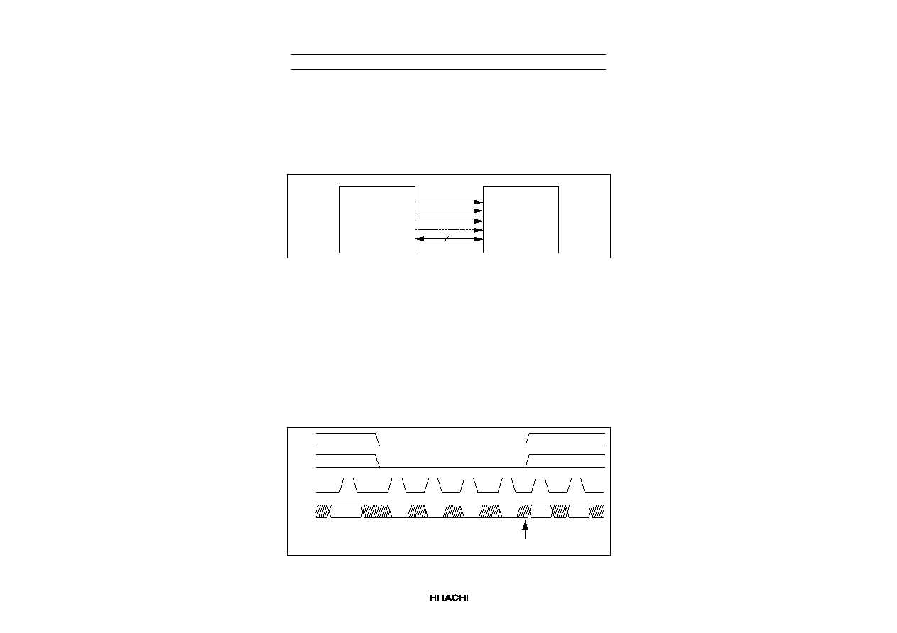
HD66740
41
Parallel Data Transfer
8-bit Bus Interface
Setting the IM2/1/0 (interface mode) to the GND/Vcc/GND level allows E-clock-synchronized 8-bit
parallel data transfer. Setting the IM2/1/0 (interface mode) to the Vcc/Vcc/GND level allows 80-
system 8-bit parallel data transfer. When the number of buses or the mounting area is limited, use a 4-
bit bus interface or serial data transfer.
C0
C1
C2
A0≠A7
E/WR*
RS
R/W / RD*
(CS*)
DB0≠DB7
H8/325
HD66740
8
*Interface via I/O port
Figure 17 Interface to 8-bit Microcomputer
4-bit Bus Interface
Setting the IM2/1/0 (interface mode) to the GND/Vcc/Vcc level allows E-clock-synchronized 4-bit
parallel data transfer using pins DB7-DB4. Setting the IM2/1/0 (interface mode) to the Vcc/Vcc/Vcc
level allows 80-system 4-bit parallel data transfer. The 8-bit instructions and RAM data are divided into
four upper/lower bits and the transfer starts from the upper four bits.
Note:
Transfer synchronization function for a 4-bit bus interface
The HD66740 supports the transfer synchronization function which resets the upper/lower
counter to count upper/lower 4-bit data transfer in the 4-bit bus interface. Noise causing
transfer mismatch between the four upper and lower bits can be corrected by a reset triggered by
consecutively writing a 0000 instruction four times. The next transfer starts from the upper
four bits. Executing synchronization function periodically can recover any runaway in the
display system.
"0000"
"0000"
"0000"
"0000"
RS
R/W
E
DB7≠
DB4
Upper
Lower
(4-bit transfer synchronization)
(1)
(2)
(3)
(4)
Upper/
lower
Figure 18 4-bit Transfer Synchronization

HD66740
42
Oscillation Circuit
The HD66740 can either be supplied with operating pulses externally (external clock mode) or oscillate
using an internal R-C oscillator with an external oscillator-resistor (external resistor oscillation mode).
Note that in R-C oscillation, the oscillation frequency is changed according to the internal capacitance
value, the external resistance value, or operating power-supply voltage. Insert the dumping registance
of about 1.5k
to prevent malfunctions caused by over-shoot or under-shoot noise in the external clock
mode.
1) External clock mode
2) External resistor oscillation mode
OSC1
OSC1
OSC2
Clock
Insert the dumping resistance.
(80 kHz)
Rf
The oscillator frequency can be
adjusted by oscillator resistor
(Rf). If Rf is increased or power
supply voltage is decreased, the
oscillation frequency decreases.
For the relationship between Rf
resistor value and oscillation
frequency, see the Electric
Characteristics Notes section.
HD66740
HD66740
1.5 k
Figure 19 Oscillation Circuits
Table 17
Relationship between Drive Duty Ratio and Frame Frequency (fosc = 75 kHz)
Display mode
1-line
Dis-
play
2-line
Dis-
play
3-line
Dis-
play
4-line
Dis-
play
5-line
Dis-
play
6-line
Dis-
play
7-line
Dis-
play
8-line
Dis-
play
9-line
Dis-
play
10-line
Dis-
play
Set value for NL3≠0
LCD Drive
0000
0001
0010
0011
0100
0101
0110
0111
1000
1001
Multiplexing
duty ratio
1/8
1/16
1/24
1/32
1/40
1/48
1/56
1/64
1/72
1/80
Drive bias
(recommend-
ed value)
1/4
1/5
1/6
1/6
1/7
1/8
1/8
1/9
1/9.5
1/10
Frame
frequency
73 Hz
73 Hz
73 Hz
73 Hz
72 Hz
74 Hz
74 Hz
73 Hz
65 Hz
59 Hz
One-frame
frequency
1,024
1,024
1,032
1,024
1,040
1,008
1,008
1,024
1,152
1,280
Note:
If the frame frequency is low and the display flickers, increase the oscillation frequency (fosc).
Particularly in the 9-line display and 10-line display modes, note that the frame frequency is
lowered.

HD66740
43
1
2
3
4
79
80
1
2
3
79
80
V1
V2
V5
GND
COM1
V2
V5
GND
COM2
1 frame
1 frame
V1
V2
V5
GND
COM79
V1
V2
V5
GND
COM80
V1
Figure 20 LCD Drive Output Waveform (B-pattern AC Drive with 1/80 Multiplexing Duty
Ratio)

HD66740
44
n-raster-row Reversed AC Drive
The HD66740 supports not only the LCD reversed AC drive in a one-frame unit (B-pattern waveform)
but also the n-raster-row reversed AC drive which alternates in an n-raster-row unit from one to 32
raster-rows (C-pattern waveform). When a problem affecting display quality occurs, such as crosstalk
at high-duty driving of more than five lines (1/40 duty), the n-raster-row reversed AC drive (C-pattern
waveform) can improve the quality. Determine the number of raster-rows n (NW bit set value + 1) for
alternating after confirmation of the display quality with the actual LCD panel. However, if the number
of AC raster-rows is reduced, the LCD alternating frequency becomes high. Because of this, the charge
or discharge current is increased in the LCD cells.
1 2 3 4 5 6 7 8 9 10 11 12 13
79 80 1 2 3 4 5 6 7 8 9 10 11 12 13
79 80 1 2 3
B-pattern
waveform drive
∑ 1/80 duty
1 frame
1 frame
C-pattern
waveform drive
∑ 1/80 duty
∑ 11-raster-row
reversal
∑ Without EORs
C-pattern
waveform drive
∑ 1/80 duty
∑ 11-raster-row
reversal
∑ With EORs
Note: Specify the number of AC drive raster-rows and the necessity of EOR so that the DC bias is not generated for
the liquid crystal.
Figure 21 Example of an AC Signal under n-raster-row Reversed AC Drive
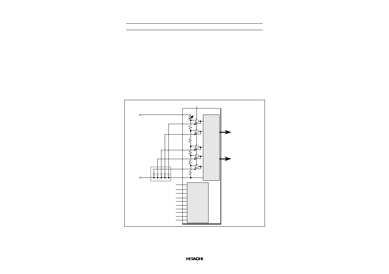
HD66740
45
Liquid Crystal Display Voltage Generator
When External Power Supply and Internal Operational Amplifiers are Used
To supply LCD drive voltage directly from the external power supply without using the internal booster,
circuits should be connected as shown in figure 22. Here, contrast can be adjusted by software through
the CT bits of the contrast adjustment register.
The HD66740 incorporates a voltage-follower operational amplifier for each V1 to V5 to reduce current
flowing through the internal bleeder-resistors, which generate different levels of liquid-crystal drive
voltages. Thus, potential differences between V
LCD
and V1 and between V5 and GND must be 0.4 V or
higher. Note that the OPOFF pin must be grounded when using the operational amplifiers. Place a
capacitor of about 0.1 µ F to 0.5 µ F between each internal operational amplifier V1OUT to V5OUT
output and GND and stabilize the output level of the operational amplifier.
C1+
V
LCD
V
LCD
VR
R
0
R
R
R
-
+
-
+
-
+
-
+
-
+
GND
Booster
OPOFF = GND
R
HD66740
V1OUT
+
V2OUT
V3OUT
V4OUT
V5OUT
+
+
+
+
LCD
driver
SEG1 to SEG112
COM1 to COM80
V1
V3
V4
V2
V5
GND
Vci
C1-
C2+
C2-
VLOUT
0.1
µ
F
to 0.5
µ
F
GND
C3+
C3-
C4+
C4-
Figure 22 External Power Supply Circuit for LCD Drive Voltage Generation

HD66740
46
When an Internal Booster and Internal Operational Amplifiers are Used
To supply LCD drive voltage using the internal booster, circuits should be connected as shown in figure
23. Here, contrast can be adjusted through the CT bits of the contrast control instruction. Temperature can
be compensated either through the CT bits or by controlling the reference voltage for the booster (Vci
pin) using a thermistor.
Note that Vci is both a reference voltage and power supply for the booster. The reference voltage must
therefore be adjusted using an emitter-follower or a similar element so that sufficient current can be
supplied. In this case, Vci must be equal to or smaller than the V
CC
level.
The HD66740 incorporates a voltage-follower operational amplifier for each of V1 to V5 to reduce
current flowing through the internal bleeder-resistors, which generate different liquid-crystal drive
voltages. Thus, the potential differences between V
LCD
and V1 and between V5 and GND must be 0.4 V
or higher.
Note that the OPOFF pin must be grounded when using the operational amplifiers. Place a capacitor of
about 0.1 µF to 0.5 µF between each internal operational amplifier V1OUT to V5OUT output and GND
and stabilize the output level of the operational amplifier.

HD66740
47
V
LCD
VR
R
0
R
R
R
-
+
-
+
-
+
-
+
-
+
GND
C1+
C1-
Vci
+
1
µ
F
1
µ
F
VLOUT
GND
+
C2+
C2-
+
Booster
OPOFF = GND
R
HD66740
V1OUT
+
V2OUT
V3OUT
V4OUT
V5OUT
+
+
+
+
LCD
driver
SEG1 to SEG112
COM1 to COM80
V1
V3
V4
V2
V5
GND
0.1
µ
F
to 0.5
µ
F
GND
Vci
C3+
C3-
+
C3+
C3-
+
1
µ
F
1
µ
F
1
µ
F
Notes: 1. The reference voltage input (Vci) must be adjusted so that the output voltage after boosting will not exceed
the absolute maximum rating for the liquid-crystal power supply voltage (17 V). Particularly, Vci must be
3.3 V or less for five-times boosting.
2. Vci is both a reference voltage and power supply for the booster; connect it to Vcc directly or combine it
with a transistor so that sufficient current can be obtained.
3. Polarized capacitors must be connected correctly.
4. Circuits for temperature compensation should be based on the sample circuit in figure 24.
Figure 23 Internal Booster for LCD Drive Voltage Generation
Vcc
Thermistor
GND
Tr
Vcc
Vci
HD66740
Figure 24 Temperature Compensation Circuit

HD66740
48
Notes on Using Internal Operational Amplifier
The HD66740 has a low-current-consumption-type operational amplifier. When a low-voltage supply
is used, particularly at low temperatures near ≠20
∞
C, the current in the operational amplifier is reduced.
Therefore, depending on the specifications or display pattern of the LCD panel used, screen quality may
be poor or the LCD panel may not operate at all.
For the operational specifications of the LCD panel, one must consider the drive condition (setting of the
VTEST pin) or the peripheral circuits of the LCD panel in conjunction with the power-supply voltage.
Pin condition for HD66740 (setting VTEST pin):
1. When the power-supply voltage is Vcc
2.5 V (i.e., the current in the operational amplifier is
sufficient), leave the VTEST pin open (disconnected).
2. When the power-supply voltage is Vcc < 2.5 V (i.e., the current is reduced in the operational
amplifier at low temperature), 1.2 to 1.3 V should be input to the VTEST pin.
The following table and figure correspond to inputs of 1.2 to 1.3 V to the VTEST pin. When higher
LCD drive current is required due to the characteristics of the LCD panel, check the screen quality and
current consumption, adjust the resistance values (R1 and R2), and increase the VTEST pin voltage.
(This is also valid when Vcc
2.5 V.)
GND
Vcc
to VTEST pin
Vtest = 1.2 to 1.3V
R1
R2
Figure 24-a Circuit to for Generating VTEST Pin Voltage
Table 17-a Settings to Generate VTEST Pin Voltage
Vcc
R1
R2
Vtest (VTEST Pin Voltage)
2.4 V
270 k
330 k
1.23 V
2.0 V
220 k
360 k
1.22 V
1.8 V
180 k
390 k
1.22 V

HD66740
49
Countermeasures for Screen Quality when Using On-chip Operational Amplifier
The HD66740 is an on-chip LCD driver that has an LCD power supply for high duty. Screen quality is
affected by the load current of the high-duty LCD panel used. When the bias (1/10 bias, 1/9.5 bias, 1/9
bias, etc.) is high and the displayed pattern is completely or almost completely white, the white sections
may appear dark.
If this happens, execute the following countermeasures to improve screen quality.
(1) After the change in the V4OUT/V3OUT level is verified, insert about 1 M
between V4OUT and
GND or VLCD and V3OUT and then adjust the screen quality (see the following figures). By
inserting resistance, the current consumption increases as much as the boosting factor of the
resistance current. Adjust the resistance after checking the screen quality and the increase in current
consumption.
(2) Decrease the drive bias and use the new bias level after verifying that the potential differences
between V4OUT and GND or VLCD and V3OUT are sufficient.
GND
VLCD
Driver
Vbn
Fixed
current
source
RV4
C
V4OUT
Figure 24-b Countermeasure for V4OUT Output
GND
VLCD
Driver
Vbp
Fixed
current
source
RV3
C
V3OUT
Figure 24-c Countermeasure for V3OUT Output
Note:
The actual LCD drive voltage-VLCD used must not exceed 15.0 V, and the absolute rating must
not exceed 16.0 V.

HD66740
50
Switching the Boosting Multiplying Factor
Instruction bits (BT1/0 bits) can optionally select the boosting multiplying factor of the internal booster.
According to the display status, power consumption can be reduced by changing the LCD drive duty and
the LCD drive bias, and by controlling the boosting multiplying factor for the minimum requirements.
For details, see the Partial-display-on Function section.
Due to the maximum boosting multiplying factor, the following external capacitor needs to be connected.
For example, when the maximum boosting is quadrupled, the capacitors between C4+ and C4≠ for five-
times boosting are not needed, so these pins must be open.
Table 18
VLOUT Output Status
BT1
BT0
VLOUT Output Status
0
0
Triple boosting output
0
1
Quadruple boosting output
1
0
Five-times boosting output
1
1
Setting inhibited
C1+
C1-
Vci
+
1
µ
F
0.47
µ
F
to 1
µ
F
VLOUT
GND
+
C2+
C2-
+
0.47
µ
F
to 1
µ
F
Vci
C3+
C3-
+
0.47
µ
F
to 1
µ
F
i) Maximum five-times boosting
ii) Maximum quadruple boosting
iii) Maximum triple boosting
C4+
C4-
+
0.47
µ
F
to 1
µ
F
C1+
C1-
Vci
+
VLOUT
GND
+
C2+
C2-
+
Vci
C3+
C3-
+
C4+
C4-
C1+
C1-
Vci
+
VLOUT
GND
+
C2+
C2-
+
Vci
C3+
C3-
C4+
C4-
0.47
µ
F
to 1
µ
F
0.47
µ
F
to 1
µ
F
0.47
µ
F
to 1
µ
F
0.47
µ
F
to 1
µ
F
0.47
µ
F
to 1
µ
F
1
µ
F
1
µ
F
Figure 25 Booster Output Multiplying Factor Switching

HD66740
51
Example of Power-supply Voltage Generator for More Than Five-times Boosting Output
The HD66740 incorporates the booster for up to five-times boosting. However, the LCD drive voltage
(VLCD) will not be enough for five-times boosting from Vcc when the power-supply voltage of Vcc is
low or when the LCD drive voltage is high for the high-contrast LCD display. In this case, the reference
voltage (Vci) for boosting can be set higher than the power-supply voltage of Vcc.
Set the Vci input voltage for the booster to 3.6 V or less within the range of Vcc + 1.0 V. Control the
Vci voltage so that the boosting output voltage (VLOUT) should be less than the absolute maximum
ratings (17 V).
+
1
µ
F
+
+
+
1
µ
F
1
µ
F
1
µ
F
SEG1 to SEG112
COM1 to COM80
C1+
C1-
Vci
1
µ
F
VLOUT
GND
+
C2+
C2-
Booster
C3+
C3-
C4+
C4-
LCD driver
Regula
-tor
(2)
Regula
-tor
(1)
Vcc
Logic circuit
2.5 V
3.0 V
VLCD
GND
GND
GND
3.0 x 5 = 15 V
Battery
3.6 V
GND (= 0 V)
Vcc (= 2.5 V)
Vcc (= 3 V)
VLCD (= 15 V)
HD66740
Figure 26 Usage Example of Booster at Vci > Vcc

HD66740
52
Contrast Adjuster
Software can adjust 64-step contrast for an LCD by varying the liquid-crystal drive voltage (potential
difference between V
LCD
and V1) through the CT bits of the contrast adjustment register (electron volume
function). The value of a variable resistor between V
LCD
and V1 (VR) can be precisely adjusted in a 0.05
x R unit within a range from 0.05 x R through 3.20 x R, where R is a reference resistance obtained by
dividing the total resistance.
The HD66740 incorporates a voltage-follower operational amplifier for each of V1 to V5 to reduce
current flowing through the internal bleeder resistors, which generate different liquid-crystal drive
voltages. Thus, CT5-0 bits must be adjusted so that the potential differences between V
LCD
and V1 and
between V5 and GND are 0.4 V or higher when liquid-crystal drives, particularly when the VR is
small.
VR
R
R
R0
R
R
GND
VLCD
-
+
-
+
-
+
-
+
-
+
HD66740
CT
V1
V2
V3
V4
V5
GND
Figure 27 Contrast Adjuster

HD66740
53
Table 19
Contrast Adjustment Bits (CT) and Variable Resistor Values
0
CT3
0
CT2
0
CT1
0
CT0
3.20 x R
CT Set Value
Variable Resistor
Value (VR)
0
0
0
1
3.15 x R
0
0
1
0
3.10 x R
0
0
1
1
3.05 x R
0
1
0
0
3.00 x R
0
1
0
1
2.95 x R
0
1
1
0
2.90 x R
0
1
1
1
2.85 x R
0
CT4
0
0
0
0
0
0
0
1
0
0
1
2.75 x R
0
1
0
1
0
2.70 x R
0
Potential Difference
between V1 and GND
Display Color
(Small)
(Large)
(Light)
(Deep)
1
0
1
2.65 x R
0
1
1
0
0
2.60 x R
0
1
1
1
1
1.65 x R
1
0
0
0
0
1.60 x R
0
0
0
0
1
1.55 x R
0
0
0
1
0
1.50 x R
0
0
0
1
1
1.45 x R
0
0
1
0
0
1.40 x R
0
0
1
0
1
1.35 x R
0
0
1
1
0
1.30 x R
0
0
1
1
1
1.25 x R
0
1
0
0
0
1.20 x R
0
1
0
0
1
1.15x R
1
1
1
0
0
0.20 x R
1
1
1
0
1
0.15 x R
1
1
1
1
0
0.10 x R
1
1
1
1
1
0.05 x R
1
1
0
0
0
2.80 x R
0
1
0
CT5
0
0
0
0
0
0
0
0
0
0
0
0
1
1
1
1
1
1
1
1
1
1
1
1
1
1
0

HD66740
54
Table 20
Contrast Adjustment per Bias Drive Voltage
9.5 x R + VR
9.5 x R
x (V
LCD
- GND)
0.748 x (V
LCD
-GND)
V
DR
0.994 x (V
LCD
-GND)
0.4 [V]
0.4 [V]
9.5 x R + VR
VR
x (V
LCD
-GND)
9.5 x R + VR
R
x (V
LCD
-GND)
5 x R + VR
5 x R
x (V
LCD
- GND)
0.610 x (V
LCD
-GND )
V
DR
0.990 x (V
LCD
-GND)
0.4 [V]
0.4 [V]
5 x R + VR
VR
x (V
LCD
-GND )
5 x R + VR
R
x (V
LCD
-GND )
4 x R + VR
4 x R
x (V
LCD
- GND)
0.556 x (V
LCD
-GND)
V
DR
0.988 x (V
LCD
-GND)
0.4 [V]
0.4 [V]
4 x R + VR
VR
x (V
LCD
-GND)
4 x R + VR
R
x (V
LCD
-GND)
9 x R + VR
9 x R
x (V
LCD
- GND)
0.737 x (V
LCD
-GND)
V
DR
0.994 x (V
LCD
-GND)
0.4 [V]
0.4 [V]
9 x R + VR
VR
x (V
LCD
-GND)
9 x R + VR
R
x (V
LCD
-GND)
10 x R + VR
10 x R
x (V
LCD
- GND)
0.757 x (V
LCD
-GND)
V
DR
0.995 x (V
LCD
-GND)
0.4 [V]
0.4 [V]
VR
x (V
LCD
-GND)
10 x R + VR
R
x (V
LCD
-GND)
10 x R + VR
Bias
LCD drive voltage: V
DR
Contrast adjustment range
1/10
bias
drive
1/9.5
bias
drive
1/9
bias
drive
1/5
bias
drive
1/4
bias
drive
- LCD drive voltage
adjustment range
- Limit of potential
difference between V5 and GND
- Limit if potential
difference between VLCD and V1
:
:
:
- LCD drive voltage
adjustment range
- Limit of potential
difference between V5 and GND
- Limit if potential
difference between VLCD and V1
:
:
:
8 x R + VR
8 x R
x (V
LCD
- GND)
0.714 x (V
LCD
-GND)
V
DR
0.993 x (V
LCD
-GND)
0.4 [V]
0.4 [V]
8 x R + VR
VR
x (V
LCD
-GND)
8 x R + VR
R
x (V
LCD
-GND)
1/8
bias
drive
- LCD drive voltage
adjustment range
- Limit of potential
difference between V5 and GND
- Limit if potential
difference between VLCD and V1
:
:
:
6 x R + VR
6 x R
x (V
LCD
- GND)
0.652 x (V
LCD
-GND)
V
DR
0.992 x (V
LCD
-GND)
0.4 [V]
0.4 [V]
VR
x (V
LCD
-GND)
6 x R + VR
6 x R + VR
R
x (V
LCD
-GND)
7 x R + VR
7 x R
x (V
LCD
- GND)
0.686 x (V
LCD
-GND)
V
DR
0.993 x (V
LCD
-GND)
0.4 [V]
0.4 [V]
VR
x (V
LCD
-GND)
7 x R + VR
R
x (V
LCD
-GND)
7 x R + VR
1/7
bias
drive
1/6
bias
drive
- LCD drive voltage
adjustment range
- Limit of potential
difference between V5 and GND
- Limit if potential
difference between VLCD and V1
:
:
:
- LCD drive voltage
adjustment range
- Limit of potential
difference between V5 and GND
- Limit if potential
difference between VLCD and V1
:
:
:
- LCD drive voltage
adjustment range
- Limit of potential
difference between V5 and GND
- Limit if potential
difference between VLCD and V1
:
:
:
- LCD drive voltage
adjustment range
- Limit of potential
difference between V5 and GND
- Limit if potential
difference between VLCD and V1
:
:
:
- LCD drive voltage
adjustment range
- Limit of potential
difference between V5 and GND
- Limit if potential
difference between VLCD and V1
:
:
:

HD66740
55
Liquid Crystal Display Drive Bias Selector
An optimum liquid crystal display bias value can be selected using BS2-0 bits, according to the liquid
crystal drive duty ratio setting (NL3-0 bits). Liquid crystal display drive duty ratio and bias value can
be displayed while switching software applications to match the LCD panel display status. The
optimum bias value calculated using the following expression is an ideal value where the optimum
contrast is obtained. Driving by using a lower value than the optimum bias value provides lower
contrast and lower liquid crystal display voltage (potential difference between V1 and GND). When the
liquid crystal display voltage is insufficient even if a five-times booster is used or output voltage is
lowered because the battery life has been reached, the display can be made easier to see by lowering the
liquid crystal bias.
The liquid crystal display can be adjusted by using the contrast adjustment register (CT4-0 bits) and
selecting the booster output level (BT1/0 bits).
Optimum bias value for 1/N duty ratio drive voltage =
1
N + 1
Table 21
Optimum Drive Bias Values
LCD drive duty ratio
1/80
1/72
1/64
1/56
1/48
1/40
1/32
1/24
1/16
1/8
(NL3-0 set value)
1001
1000
0111
0110
0101
0100
0011
0010
0001
0000
Optimum drive bias
value
1/10
1/9.5
1/9
1/8
1/8
1/7
1/6
1/6
1/5
1/4
(BS2-0 set value)
000
001
010
011
011
100
101
101
110
111

HD66740
56
VR
V1
V2
V3
V4
V5
R
R
6R
R
R
V1
V2
V3,V4
V5
GND
R
R
R
R
i) 1/ 10 bias
(BS2≠0 = 000)
vi) 1/ 4 bias
(BS2≠0 = 111)
GND
VR
VLCD
VLCD
Note: R = Reference resistor
VR
V1
V2
V3
V4
V5
R
R
5.5R
R
R
ii) 1/ 9.5 bias
(BS2≠0 = 001)
VLCD
VR
V1
V2
V3
V4
V5
R
R
5R
R
R
iii) 1/ 9 bias
(BS2≠0 = 010)
VLCD
VR
V1
V2
V3
V4
V5
R
R
4R
R
R
iv) 1/ 8 bias
(BS2≠0 = 011)
VLCD
VR
GND
V1
V2
V3
V4
V5
R
R
3R
R
R
v) 1/7 bias
(BS2≠0 = 100)
VLCD
GND
GND
GND
GND
GND
GND
GND
GND
GND
VR
GND
V1
V2
V3
V4
V5
R
R
2R
R
R
v) 1/6 bias
(BS2≠0 = 101)
VLCD
GND
VR
GND
V1
V2
V3
V4
V5
R
R
R
R
R
v) 1/5 bias
(BS2≠0 = 110)
VLCD
GND
Figure 28 Liquid Crystal Display Drive Bias Circuit

HD66740
57
LCD Panel Interface
The HD66740 has a function for changing the common driver/segment driver output shift direction using
the CMS bit and SGS bit to meet the chip mounting positions of the HD66740. This is to facilitate the
interface wiring to the LCD panel with COG or TCP installed.
Back of chip
∑ CMS = 0
∑ SGS = 0
SEG112/1
SEG1/112
SEG1/112
SEG112/1
COM9/72
SEG1/112
SEG112/1
HITACHI Ltd.
LCD Controller/
Driver:HD66740
>112 x 80 dots
Graphisc display
>16 x 10 chracter
display
>
>x4 Booster
>Op-amp
Front of chip
∑ CMS = 0
∑ SGS = 1
COM1/80
COM72/9
SEG112/1
SEG1/112
COM9/72
Front of chip
∑ CMS = 1
∑ SGS = 0
Back of chip
∑ CMS = 1
∑ SGS = 1
COM41/40
COM72/9
COM80/1
COM1/80
COM8/73
COM80/1
8
32
COM9/72
COM80/1
COM1/80
COM72/9
COM41/40
COM8/73
COM73/8
COM40/41
COM72/9
COM1/80
COM8/72
COM80/1
COM73/8
COM40/41
HITACHI Ltd.
LCD Controller/
Driver:HD66740
>112 x 80 dots
Graphisc display
>16 x 10 chracter
display
>
>x4 Booster
>Op-amp
HITACHI Ltd.
LCD Controller/
Driver:HD66740
>112 x 80 dots
Graphisc display
>16 x 10 chracter
display
>
>x4 Booster
>Op-amp
HITACHI Ltd.
LCD Controller/
Driver:HD66740
>112 x 80 dots
Graphisc display
>16 x 10 chracter
display
>
>x4 Booster
>Op-amp
COM73/8
COM40/41
8
32
8
32
COM41/40
COM8/73
8
32
COM73/8
COM40/41
8
32
COM41/40
COM8/73
8
32
8
32
8
32
Figure 29 1/80 Duty Drive Pattern Wiring
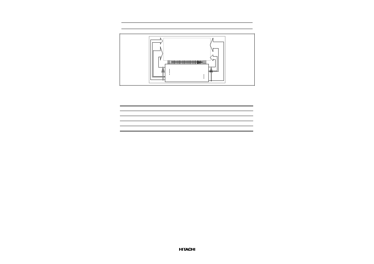
HD66740
58
LCD PANEL
Front of chip
∑ CMS = 0
∑ SGS = 1
COM1/80
COM72/9
SEG112/1
SEG1/112
COM9/72
COM41/40
COM8/73
COM80/1
COM73/8
COM40/41
Figure 30 1-line Display Pattern Wiring
Table 22 Number of Left and Right Extension Lines of Common Driver
Drive Duty Ratio
Left Edge of Screen
Right Edge of Screen
1/48
16 (COM1≠8, 41≠48)
32 (COM9≠40)
1/56
24 (COM1≠8, 41≠56)
32 (COM9≠40)
1/64
32 (COM1≠8, 41≠64)
32 (COM9≠40)
1/72
40 (COM1≠8, 41≠72)
32 (COM9≠40)
1/80
40 (COM1≠8, 41≠72)
40 (COM9≠40, 73≠80)

HD66740
59
Graphics Display Function
In the graphics display mode, kanji characters, special symbols, and graphics icons can be displayed.
Up to 112 x 80-dot display is allowed using the CGRAM. Thus, for a 12 x 13-dot kanji font, up to a
6-line x 9-character kanji display, and for a 14 x 15-dot kanji font, up to a 6-line x 8-character kanji
display, and for a 16 x 16-dot kanji font, up to a 5-line x 6-character kanji display are allowed.
i) 12 x 13-dot kanji display
example
(6-line x 9-character display)
ii) 112 x 80-dot game display
example
Figure 31 Display Example in Graphics Display Mode
Vertical Smooth Scroll Display
The HD66740 can scroll character and graphics display vertically in units of raster-rows. This is
achieved by writing display data into a one-line area that is not being used for display. In other words,

HD66740
60
one line can be used to achieve continuous smooth vertical scroll even in a 9-line or less display. Here,
after the 10th line is displayed, the first line is displayed again. When the 10th line is fully displayed, all
one-line display data must be rewritten immediately after scrolling because there is no non-displayed
area. Additionally, when display areas of a graphics icon such as a pictogram or a menu bar are partially
fixed-displayed, the remaining areas can be displayed. For details, see the Partial Smooth Scroll Display
Function section.
Specifically, this function is controlled by incrementing or decrementing the value in the display-start
line bits (SL2 to SL0) and display-start raster-row bits (SN3 to SN0) by 1. For example, to smoothly
scroll up, first set line bits SN3 to SN0 to 0000, and increment SL2 to SL0 by 1 from 000 to 111 to scroll
seven raster-rows. Then increment line bits SN3 to SN0 to 0001, and again increment SL2 to SL0 by 1
from 000 to 111. If the vertical double-height display is at the top of the line, scrolling is done by each
two raster-row.
When the response speed of the liquid crystal is low or when high-speed scrolling is needed, two- to
four-raster-row scrolling is recommended.

HD66740
61
Setting Instructions (10-line Display: NL3-0 = 1001)
DB7 DB6DB5 DB4 DB3 DB2DB1 DB0
R/W RS
0
0
0
1
0
Scroll up display
Set 96 x 80-dot initial display data to CGRAM
CPU Wait
0
0
1
0
0
0
0
1
0
0
0
0
1
0
0
0
0
1
0
0
0
0
1
0
0
0
0
1
0
0
1
0
1
0
0
0
0
1
0
0
1
1
0
0
0
0
1
0
0
0
0
1
0
0
0
0
1
0
0
0
0
1
0
0
0
Update 1st-line (address 000 to 05FH) display data in CGRAM
CPU Wait
CPU Wait
0
0
0
1
0
0
1
0
1
0
0
0
0
1
0
1
0
1
0
0
0
0
1
0
0
0
0
1
0
0
0
0
1
0
0
0
0
0
CPU Wait
CPU Wait
0
0
0
1
0
0
1
0
1
0
0
0
0
1
0
1
1
1
0
0
0
0
1
0
0
0
0
1
0
0
0
0
1
0
0
0
0
0
CPU Wait
0
0
0
1
0
0
1
0
1
0
SN3≠SN0 = 0000
SL2≠SL0 = 000
(1st raster-row of 1st line displayed at the top)
Scroll up 4 raster-rows
(5th raster-row of 1st line displayed at the top)
SN3≠SN0 = 0001
(1st raster-row of 2nd line displayed at the top)
SL2≠SL0 = 000
Update 1st-line (address 000 to 05FH) display data in CGRAM
Scroll up 12 raster-rows
(5th raster-row of 2nd line displayed at the top)
Update 2nd-line (address 100 to 15FH) display data in CGRAM
SN3≠SN0 = 0010
SL2≠SL0 = 000
(1st raster-row of 3rd line displayed at the top)
Update 2nd-line (address 100 to 15FH) display data in CGRAM
Scroll up 20 raster-rows
(5th raster-row of 3rd line displayed at the top)
Update 3rd-line (address 200 to 25FH) display data in CGRAM
SN3≠SN0 = 0011
SL2≠SL0 = 000
(1st raster-row of 4th line displayed at the top)
Update 3rd-line (address 200 to 25FH) display data in CGRAM
Scroll up 28 raster-rows
(5th raster-row of 4th line displayed at the top)
Update 4th-line (address 300 to 35FH) display data in CGRAM
CPU Wait
Figure 32 Setting Instructions for Vertical Smooth Scroll

HD66740
62
Partial Smooth Scroll Display Function
The HD66740 can partially fixed-display the areas of a graphics icon, such as a pictogram or a menu bar,
and perform vertical smooth scrolling of the remaining bit-map areas. Since the PS1 to PS0 bits do not
perform smooth scrolling of the upper first to third display lines but does fixed-display, pictograms can
be placed. When CN1 to CN0 bits are set to 10, the first line is displayed at the bottom edge of the LCD
screen, and the menu bar can be fixed-displayed at the bottom. This function can largely control the
bit-map rewrite frequencies and reduce software loads.

HD66740
63
Table 23 Bit Setting and Display Lines
1st line
2nd line
3rd line
4th line
5th line
6th line
7th line
8th line
9th line
10th line
PS1≠0
= 00
SN3≠0
= 0000
SN3≠0
= 0001
SN3≠0
= 0010
COM1
COM80
PS1≠0
= 01
COM1
COM80
PS1≠0
= 10
COM1
COM80
PS1≠0
= 11
COM1
COM80
SN3≠0
= 0011
SN3≠0
= 0011
SN3≠0
= 0100
CN1≠0 = 00
Bit
Setting
COM
Position
CN1≠0 = 10
SN3≠0
= 0000
SN3≠0
= 0001
SN3≠0
= 0010
SN3≠0
= 0011
2nd line
3rd line
4th line
5th line
6th line
7th line
8th line
9th line
10th line
1st line
3rd line
4th line
5th line
6th line
7th line
8th line
9th line
10th line
1st line
2nd line
4th line
5th line
6th line
7th line
8th line
9th line
10th line
1st line
2nd line
3rd line
5th line
6th line
7th line
8th line
9th line
10th line
1st line
3rd line
4th line
2nd line
2nd line
3rd line
4th line
5th line
6th line
7th line
8th line
9th line
10th line
1st line
3rd line
4th line
5th line
6th line
7th line
8th line
9th line
10th line
1st line
2nd line
4th line
5th line
6th line
7th line
8th line
9th line
10th line
1st line
2nd line
3rd line
5th line
6th line
7th line
8th line
9th line
10th line
1st line
3rd line
4th line
2nd line
6th line
7th line
8th line
9th line
10th line
1st line
2nd line
3rd line
4th line
5th line
1st line
2nd line
3rd line
4th line
5th line
6th line
7th line
8th line
9th line
1st line
1st line
2nd line
3rd line
4th line
5th line
6th line
7th line
8th line
9th line
10th line
1st line
1st line
1st line
3rd line
4th line
5th line
6th line
7th line
8th line
9th line
10th line
2nd line
4th line
5th line
6th line
7th line
8th line
9th line
10th line
2nd line
3rd line
5th line
6th line
7th line
8th line
9th line
10th line
2nd line
3rd line
4th line
1st line
2nd line
3rd line
4th line
5th line
6th line
7th line
8th line
9th line
1st line
1st line
2nd line
3rd line
4th line
5th line
6th line
7th line
8th line
9th line
10th line
1st line
3rd line
4th line
5th line
6th line
7th line
8th line
9th line
10th line
2nd line
4th line
5th line
6th line
7th line
8th line
9th line
10th line
2nd line
3rd line
1st line
1st line
5th line
6th line
7th line
8th line
9th line
10th line
2nd line
3rd line
4th line
1st line
2nd line
1st line
2nd line
1st line
2nd line
1st line
2nd line
1st line
2nd line
1st line
2nd line
3rd line
4th line
5th line
6th line
7th line
8th line
2nd line
3rd line
4th line
5th line
6th line
7th line
8th line
9th line
3rd line
4th line
5th line
6th line
7th line
8th line
9th line
10th line
4th line
5th line
6th line
7th line
8th line
9th line
10th line
3rd line
5th line
6th line
7th line
8th line
9th line
3rd line
4th line
10th line
2nd line
2nd line
2nd line
2nd line
2nd line
1st line
2nd line
3rd line
4th line
5th line
6th line
7th line
8th line
1st line
1st line
1st line
1st line
1st line
2nd line
3rd line
4th line
5th line
6th line
7th line
8th line
9th line
3rd line
4th line
5th line
6th line
7th line
8th line
9th line
10th line
4th line
5th line
6th line
7th line
8th line
9th line
10th line
3rd line
5th line
6th line
7th line
8th line
9th line
3rd line
4th line
10th line
1st line
2nd line
3rd line
1st line
2nd line
3rd line
1st line
2nd line
3rd line
1st line
2nd line
3rd line
1st line
2nd line
3rd line
1st line
2nd line
3rd line
4th line
5th line
6th line
7th line
2nd line
3rd line
4th line
5th line
6th line
7th line
8th line
3rd line
4th line
5th line
6th line
7th line
8th line
9th line
4th line
5th line
6th line
7th line
8th line
9th line
10th line
5th line
6th line
7th line
8th line
9th line
10th line
4th line
2nd line
3rd line
2nd line
3rd line
2nd line
3rd line
2nd line
3rd line
2nd line
3rd line
1st line
2nd line
3rd line
4th line
5th line
6th line
7th line
1st line
1st line
1st line
1st line
1st line
2nd line
3rd line
4th line
5th line
6th line
7th line
8th line
3rd line
4th line
5th line
6th line
7th line
8th line
9th line
4th line
5th line
6th line
7th line
8th line
9th line
10th line
5th line
6th line
7th line
8th line
9th line
10th line
4th line
Notes: 1. The shadow lines above are fixed-displayed. They do not depend on the setting values of the
SN3≠0 or SL3≠0 bits.
2. The SN3≠0 and SL3≠0 bits specify the next first scroll display line of the fixed-displayed lines.
3. When the drive duty ratio is nine lines (1/72 duty ratio) or less and CN1≠0 is 10, the first line
shifts to the last displayed line.

HD66740
64
Partial Smooth Scroll Display Examples
Table 24 Data Setting to the CGRAM Partial Smooth Scroll Display Examples
CGRAM Address
CGRAM Data
"000" to "06F"
"080" to "0EF"
"100" to "16F"
"180" to "1EF"
"200" to "26F"
"280" to "2EF"
"300" to "36F"
"380" to "3EF"
"400" to "46F"
"480" to "4EF"
i) Initial screen display
- PS1-0 = "10" : Fixed-displays the first and second lines
- CN1-0 = "10" : Moves the first line to the bottom edge
- SN3-0 = "0010" : Starts display from the third line
- SL2-0 = "000"
2nd line
(fixed display)
Scroll area
3rd line
(Display start position)
1st line
(fixed display)
Figure 33 Example of Initial Screen in the Partial Smooth Scroll Mode

HD66740
65
Fixed display
(2nd line)
ii) Four-dot partial scroll up
- PS1-0 = "10" : Fixed-displays the first and second lines
- CN1-0 = "10" : Moves the first line to the bottom edge
- SN3-0 = "0010" : Starts display from the third line
- SL2-0 = "100" : Shifts up by 4 dots
Display start
setting position
Fixed display
(1st line)
Figure 34 Example of Display Screen in the Partial Smooth Scroll Mode (1)
Fixed display
(2nd line)
iii) 8-dot partial scroll up
- PS1-0 = "10" : Fixed-displays the first and second lines
- CN1-0 = "10" : Moves the first line to the bottom edge
- SN3-0 = "0011" : Starts display from the fourth line
- SL2-0 = "000"
Display start
setting position
Fixed display
(1st line)
Figure 35 Example of Display Screen in the Partial Smooth Scroll Mode (2)

HD66740
66
Double-height Display
The HD66740 can double the height of any desired line from the first to 10th lines. A line can be selected
by the DL1 to DL10 bits as listed in table 25. All graphics display patterns stored in the CGRAM can be
doubled in height, allowing easy recognition. Note that there should be no space between the lines for
double-height display (figure 36).
In vertical smooth scrolling, when the display-start setting line is displaying at double height, scrolling
can be done by each two-line (dot).
Table 25 Double-height Display Specifications
Bit Setting
Display Position
DL1 = 1
1st line: double-height
DL2 = 1
2nd line: double-height
DL3 = 1
3rd line: double-height
DL4 = 1
4th line: double-height
DL5 = 1
5th line: double-height
DL6 = 1
6th line: double-height
DL7 = 1
7th line: double-height
DL8 = 1
8th line: double-height
DL9 = 1
9th line: double-height
DL10 = 1
10th line: double-height
Double height
display
(2nd line)
Double height
display
(8th line)
- NL3-0 = "1001" (10-line display)
- DL2 = 1
- DL8 = 1
Figure 36 Double-height Display (2nd and 8th Lines)

HD66740
67
Reversed Display Function
The HD66740 can display character/graphics display sections by black-and-white reversal. Black-
and-white reversal can be easily displayed when REV is set to 1.
REV = 1 (Reversed display)
Figure 37 Reversed Display

HD66740
68
Partial-display-on Function
The HD66740 can program the liquid crystal display drive duty ratio setting (NL3-0 bits), liquid crystal
display drive bias value selection (BS2-0 bits), boost output level selection (BT1/0 bit) and contrast
adjustment (CT5-0 bits). For example, in the 10-line display mode (1/80 duty ratio), the HD66740 can
selectively drive only the center of the screen or only the top or bottom of the screen by combining these
register functions and the centering display (CN1≠0 bit) function. This is called partial-display-on.
Lowering the liquid crystal display drive duty ratio as required saves the liquid crystal display drive
voltage, thus reducing internal current consumption. This is suitable for four-line display of a calendar
or time, or the display of only graphics icons (pictograms) at the top or bottom of the screen, which needs
to be continuous in the system standby state with minimal current consumption. Here, the non-
displayed lines are constantly driven by the unselected level voltage, thus turning off the LCD for the
lines.
In general, lowering the liquid crystal display drive duty ratio decreases the optimum liquid crystal
display drive voltage and liquid crystal display drive bias value. This reduces output multiplying
factors in the booster and greatly controls consumption current.
Table 26 Partial-display-on Function (10-line Display)
Item
Normal 10-line Display
Partial-on Display (Limited 4-line Display)
LCD screen
10th line displayed
Only four lines on the
center of the screen
(from the 3rd to 6th lines)
Only four lines at the top
and bottom of the screen
(from the 1st to 3rd and
10th lines)
LCD drive position
shift
Not necessary
(CN1≠0 = 00)
Necessary
(CN1≠0 = 01)
Necessary
(CN1≠0 = 01)
LCD drive duty ratio
1/80 (NL3≠0 = 1001)
1/32 (NL3≠0 = 0011)
1/32 (NL3≠0 = 0011)
LCD drive bias
value (optimum)
1/10 (BS2-0 = 000)
1/6 (BS2-0 = 101)
1/6 (BS2-0 = 101)
LCD drive voltage*
12 V to 15 V
(adjustable using CT5≠0)
6 V to 8 V
(adjustable using
CT5≠0)
6 V to 8 V
(adjustable using
CT5≠0)
Boosting output
multiplying factor
Five times (BT1≠0 = 10)
Triple (BT1≠0 = 00)
Triple (BT1≠0 = 00)
Frame frequency
(fosc = 90 kHz)
70 Hz
88 Hz
88 Hz
Note:
The LCD drive voltage depends on the LCD materials which are actually used. Since the LCD
drive voltage is high when the LCD drive duty ratio is high, a low duty ratio is suitable for low-power
consumption.

HD66740
69
- 1/32 duty drive at the top and bottom of the screen
Always applying
non-selection
level
Figure 38 Partial-on Display (Date and Time Indicated) (1)
- 1/32 duty drive at the center of the screen
Always applying
selection level
Figure 39 Partial-on Display (Date and Time Indicated) (2)

HD66740
70
Sleep Mode
Setting the sleep mode bit (SLP) to 1 puts the HD66740 in the sleep mode, where the device stops all
internal display operations, thus reducing current consumption. Specifically, LCD drive is completely
halted. Here, all the SEG (SEG1 to SEG112) and COM (COM1 to COM80) pins output the GND level,
resulting in no display. If the AMP bit is set to 0 in the sleep mode, the LCD drive power supply can be
turned off, reducing the total current consumption of the LCD module.
Table 27 Comparison of Sleep Mode and Standby Mode
Function
Sleep Mode (SLP = 1)
Standby Mode
(STB = 1)
LCD control
Turned off
Turned off
R-C oscillation circuit
Operates normally
Halted

HD66740
71
Standby Mode
Setting the standby mode bit (STB) to 1 puts the HD66740 in the standby mode, where the device stops
completely, halting all internal operations including the R-C oscillation circuit, thus further reducing
current consumption compared to that in the sleep mode. Specifically, character and segment displays,
which are controlled by the multiplexing drive method, are completely halted. Here, all the SEG (SEG1
to SEG112) and COM (COM1 to COM80) pins output the GND level, resulting in no display. If the
AMP bit is set to 0 in the standby mode, the LCD drive power supply can be turned off.
During the standby mode, no instructions can be accepted other than the start-oscillation. To cancel the
standby mode, issue the start-oscillation instruction to stabilize R-C oscillation before setting the STB bit
to 0.
Set standby mode: STB = 1
Standby mode
Issue the start-oscillation instruction
Wait at least 10 ms
Cancel standby mode: STB = 0
Turn on the LCD drive power supply: AMP = 1
Turn off the LCD power supply: AMP = 0
Figure 40 Procedure for Setting and Canceling Standby Mode

HD66740
72
Absolute Maximum Ratings
Item
Symbol
Unit
Value
Notes*
Power supply voltage (1)
V
CC
V
≠0.3 to +4.6
1, 2
Power supply voltage (2)
V
LCD
≠ GND
V
≠0.3 to +16.0
1, 3
Input voltage
Vt
V
≠0.3 to V
CC
+ 0.3
1
Operating temperature
Topr
∞C
≠40 to +85
1, 4
Storage temperature
Tstg
∞C
≠55 to +110
1, 5
Notes: 1. If the LSI is used above these absolute maximum ratings, it may become permanently
damaged. Using the LSI within the following electrical characteristics limits is strongly
recommended for normal operation. If these electrical characteristic conditions are also exceeded,
the LSI will malfunction and cause poor reliability.
2. VCC > GND must be maintained.
3. VLCD > GND must be maintained.
4. For bare die and wafer products, specified up to 85∞C.
5. This temperature specifications apply to the TCP package.

HD66740
73
DC Characteristics (V
CC
= 1.8 to 3.6 V, Ta = ≠40 to +85∞C*
1
)
Item
Symbol Min
Typ
Max
Unit Test Condition
Notes
Input high voltage
V
IH
0.7 V
CC
--
V
CC
V
2, 3
Input low voltage
V
IL
≠0.3
--
0.15 V
CC
V
V
CC
= 1.8 to 2.7 V
2, 3
Input low voltage
V
IL
≠0.3
--
0.15 V
CC
V
V
CC
= 2.7 to 3.6 V
2, 3
Output high voltage
(SDA, DB0-7 pins)
V
OH1
0.75 V
CC
--
--
V
I
OH
= ≠0.1 mA
2, 4
Output low voltage
(SDA, DB0-7 pins)
V
OL1
--
--
0.2 V
CC
V
V
CC
= 1.8 to 2.7 V,
I
OL
= 0.1 mA
2
Output low voltage
(SDA, DB0-7 pins)
V
OL1
--
--
0.15 V
CC
V
V
CC
= 2.7 to 3.6 V,
I
OL
= 0.1 mA
2
Driver ON resistance
(COM pins)
R
COM
--
3
20
k
±Id = 0.05 mA,
V
LCD
= 10 V
5
Driver ON resistance
(SEG pins)
R
SEG
--
3
30
k
±Id = 0.05 mA,
V
LCD
= 10 V
5
I/O leakage current
I
Li
≠1
--
1
µA
Vin = 0 to V
CC
6
Pull-up MOS current
(DB0-7, SDA pins)
-I
p
1
10
40
µA
V
CC
= 3 V, Vin = 0 V
2
Current consumption
during normal operation
(V
CC
≠GND)
I
OP
--
32
55
µA
R-C oscillation,
V
CC
= 3 V, Ta = 25 ∞C, f
OSC
= 86 kHz (1/72 duty)
7, 8
Current consumption
during sleep mode
(V
CC
≠GND)
I
SL
--
11
--
µA
R-C oscillation,
V
CC
= 3 V, Ta = 25 ∞C, f
OSC
= 86 kHz (1/72 duty)
7, 8
Current consumption
during standby mode
(V
CC
≠GND)
I
ST
--
0.1
5
µA
V
CC
= 3 V, Ta = 25∞C
7, 8
LCD drive power supply
current (V
LCD
≠GND)
I
LCD
--
20
35
µA
V
LCD
= 12 V,
Ta = 25 ∞C, f
OSC
= 86 kHz,
1/9 bias, VTEST3="High"
8
LCD drive voltage
(V
LCD
≠ GND)
V
LCD
4.5
--
15.0
V
9
Note:
For the numbered notes, refer to the Electrical Characteristics Notes section following these
tables.

HD66740
74
Booster Characteristics
Item
Symbol
Min
Typ
Max
Unit
Test Condition
Notes
Triple-boost
output voltage
(VLOUT pin)
V
UP3
8.5
8.9
9.0
V
V
CC
= Vci = 3.0 V,
I
O
= 30 µA, C = 1 µF,
f
OSC
= 86 kHz, Ta = 25∞C
12
Quadruple-
boost output
voltage (VLOUT
pin)
V
UP4
11.5
11.8
12.0
V
V
CC
= Vci = 3.0 V,
I
O
= 30 µA, C = 1 µF,
f
OSC
= 86 kHz, Ta = 25∞C
12
Five-times-
boost output
voltage (VLOUT
pin)
V
UP5
14.5
14.8
15.0
V
V
CC
= Vci = 3.0 V,
I
O
= 30 µA, C = 1 µF,
f
OSC
= 86 kHz, Ta = 25∞C
12
Use range of
boost output
voltage
V
UP3
,
V
UP4
,
V
UP5
V
CC
--
15.0
V
For triple to Five-times
boost
12
Note:
For the numbered notes, refer to the Electrical Characteristics Notes section following these
tables.

HD66740
75
AC Characteristics (V
CC
= 1.8 to 3.6 V, Ta = ≠40 to +85∞C*
1
)
Clock Characteristics (V
CC
= 1.8 to 3.6 V)
Item
Symbol
Min
Typ
Max
Unit
Test Condition
Notes
External clock
frequency
fcp
50
75
100
kHz
10
External clock duty
ratio
Duty
45
50
55
%
10
External clock rise
time
trcp
--
--
0.2
µs
10
External clock fall
time
tfcp
--
--
0.2
µs
10
R-C oscillation clock
f
OSC
69
86
103
kHz
Rf = 270 k
,
V
CC
= 3 V
11
Note:
For the numbered notes, refer to the Electrical Characteristics Notes section following these
tables.
68-system Bus Interface Timing Characteristics
(Vcc = 1.8 to 2.7 V)
Item
Symbol
Min
Typ
Max
Unit
Test Condition
Enable cycle time
Write
t
CYCE
600
--
--
ns
Figure 47
Read
t
CYCE
800
--
--
Enable high-level pulse width
Write
PW
EH
120
--
--
ns
Figure 47
Read
PW
EH
350
--
--
Enable low-level pulse width
Write
PW
EL
300
--
--
ns
Figure 47
Read
PW
EL
300
--
--
Enable rise/fall time
t
Er
, t
Ef
--
--
25
ns
Figure 47
Setup time (RS, R/W to E, CS*)
t
ASE
50
--
--
ns
Figure 47
Address hold time
t
AHE
20
--
--
ns
Figure 47
Write data setup time
t
DSWE
60
--
--
ns
Figure 47
Write data hold time
t
HE
20
--
--
ns
Figure 47
Read data delay time
t
DDRE
--
--
300
ns
Figure 47
Read data hold time
t
DHRE
5
--
--
ns
Figure 47

HD66740
76
(Vcc = 2.7 to 3.6 V)
Item
Symbol
Min
Typ
Max
Unit
Test Condition
Enable cycle time
Write
t
CYCE
380
--
--
ns
Figure 47
Read
t
CYCE
500
--
--
Enable high-level pulse width
Write
PW
EH
70
--
--
ns
Figure 47
Read
PW
EH
250
--
--
Enable low-level pulse width
Write
PW
EL
150
--
--
ns
Figure 47
Read
PW
EL
150
--
--
Enable rise/fall time
t
Er
, t
Ef
--
--
25
ns
Figure 47
Setup time (RS, R/W to E, CS*)
t
ASE
50
--
--
ns
Figure 47
Address hold time
t
AHE
20
--
--
ns
Figure 47
Write data setup time
t
DSWE
60
--
--
ns
Figure 47
Write data hold time
t
HE
20
--
--
ns
Figure 47
Read data delay time
t
DDRE
--
--
200
ns
Figure 47
Read data hold time
t
DHRE
5
--
--
ns
Figure 47

HD66740
77
80-system Bus Interface Timing Characteristics
(Vcc = 1.8 to 2.7 V)
Item
Symbol
Min
Typ
Max
Unit
Test Condition
Bus cycle time
Write
t
CYCW
600
--
--
ns
Figure 48
Read
t
CYCR
800
--
--
ns
Figure 48
Write low-level pulse width
PW
LW
120
--
--
ns
Figure 48
Read low-level pulse width
PW
LR
350
--
--
ns
Figure 48
Write high-level pulse width
PW
HW
300
--
--
ns
Figure 48
Read high-level pulse width
PW
HR
300
--
--
ns
Figure 48
Write/Read rise/fall time
t
WRr
,
WRf
--
--
25
ns
Figure 48
Setup time (RS to CS*, WR*, RD*)
t
AS
50
--
--
ns
Figure 48
Address hold time
t
AH
20
--
--
ns
Figure 48
Write data setup time
t
DSW
60
--
--
ns
Figure 48
Write data hold time
t
H
20
--
--
ns
Figure 48
Read data delay time
t
DDR
--
--
300
ns
Figure 48
Read data hold time
t
DHR
5
--
--
ns
Figure 48
(Vcc = 2.7 to 3.6 V)
Item
Symbol
Min
Typ
Max
Unit
Test Condition
Bus cycle time
Write
t
CYCW
380
--
--
ns
Figure 48
Read
t
CYCR
500
--
--
ns
Figure 48
Write low-level pulse width
PW
LW
70
--
--
ns
Figure 48
Read low-level pulse width
PW
LR
250
--
--
ns
Figure 48
Write high-level pulse width
PW
HW
150
--
--
ns
Figure 48
Read high-level pulse width
PW
HR
150
--
--
ns
Figure 48
Write/Read rise/fall time
t
WRr, WRf
--
--
25
ns
Figure 48
Setup time (RS to CS*, WR*, RD*)
t
AS
50
--
--
ns
Figure 48
Address hold time
t
AH
20
--
--
ns
Figure 48
Write data setup time
t
DSW
60
--
--
ns
Figure 48
Write data hold time
t
H
20
--
--
ns
Figure 48
Read data delay time
t
DDR
--
--
200
ns
Figure 48
Read data hold time
t
DHR
5
--
--
ns
Figure 48
HD66740
78
Clock-synchronized Serial Interface Timing Characteristics (V
CC
= 1.8 to 3.6 V)
(V
CC
= 1.8 to 2.55 V)
Item
Symbol
Min
Typ
Max
Unit
Test Condition
Serial clock cycle time
At write
(receive)
t
SCYC
0.5
--
20
µs
Figure 49
At read
(send)
t
SCYC
1
--
20
µs
Figure 49
Serial clock high-level width
At write
(receive)
t
SCH
230
--
--
ns
Figure 49
At read
(send)
t
SCH
480
--
--
ns
Figure 49
Serial clock low-level width
At write
(receive)
t
SCL
230
--
--
ns
Figure 49
At read
(send)
t
SCL
480
--
--
ns
Figure 49
Serial clock rise/fall time
t
scf
, t
scr
--
--
20
ns
Figure 49
Chip select setup time
t
CSU
60
--
--
ns
Figure 49
Chip select hold time
t
CH
200
--
--
ns
Figure 49
Serial input data setup time
t
SISU
100
--
--
ns
Figure 49
Serial input data hold time
t
SIH
100
--
--
ns
Figure 49
Serial output data delay time
t
SOD
--
--
400
ns
Figure 49
Serial output data hold time
t
SOH
5
--
--
ns
Figure 49

HD66740
79
(V
CC
= 2.55 to 3.6 V)
Item
Symbol
Min
Typ
Max
Unit
Test Condition
Serial clock cycle time
At write
(receive)
t
SCYC
0.2
--
20
µs
Figure 49
At read
(send)
t
SCYC
0.5
--
20
µs
Figure 49
Serial clock high-level width
At write
(receive)
t
SCH
80
--
--
ns
Figure 49
At read
(send)
t
SCH
230
--
--
ns
Figure 49
Serial clock low-level width
At write
(receive)
t
SCL
80
--
--
ns
Figure 49
At read
(send)
t
SCL
230
--
--
ns
Figure 49
Serial clock rise/fall time
t
scf
, t
scr
--
--
20
ns
Figure 49
Chip select setup time
t
CSU
60
--
--
ns
Figure 49
Chip select hold time
t
CH
200
--
--
ns
Figure 49
Serial input data setup time
t
SISU
40
--
--
ns
Figure 49
Serial input data hold time
t
SIH
40
--
--
ns
Figure 49
Serial output data delay time
t
SOD
--
--
200
ns
Figure 49
Serial output data hold time
t
SOH
5
--
--
ns
Figure 49
Reset Timing Characteristics (V
CC
= 1.8 to 3.6 V)
Item
Symbol
Min
Typ
Max
Unit
Test Condition
Reset low-level width
t
RES
1
--
--
ms
Figure 50

HD66740
80
I2C Bus Interface Timing Characteristics
(Vcc = 1.8 to 3.6 V)
Item
Symbol Min
Typ
Max
Unit
Test Condition
SCL clock frequency
f
SCL
0
--
1300
kHz
Figure 51
SCL clock high-level pulse width
t
SCLH
120
--
--
ns
Figure 51
SCL clock low-level pulse width
t
SCLL
240
--
--
ns
Figure 51
SCL/SDA rise time
t
Sr
10
--
160
ns
Figure 51
SCL/SDA fall time
t
Sf
10
--
70
ns
Figure 51
Bus free time
t
BUF
240
--
--
ns
Figure 51
Start condition hold time
t
STAH
320
--
--
ns
Figure 51
Setup time for a repeated START
condition
t
STAS
320
--
--
ns
Figure 51
Setup time for STOP condition
t
STOS
320
--
--
ns
Figure 51
SDA data setup time
t
SDAS
40
--
--
ns
Figure 51
SDA data hold time
t
SDAH
0
--
--
ns
Figure 51
SCL/SDA spike pulse width
t
SP
0
--
10
ns
Figure 51

HD66740
81
Electrical Characteristics Notes
1. For bare die products, specified up to 85∞C.
2. The following three circuits are I/O pin configurations (figure 41).
Pins: RESET*, CS*, E/WR*/SCL, RS,
OSC1, OPOFF, IM2/1, IM0/ID, TEST
Pin: OSC2
PMOS
NMOS
Vcc
GND
Pin: RW/RD*/SDA
PMOS
NMOS
Vcc
GND
NMOS
PMOS
Vcc
(Pull-up MOS)
Vcc
Vcc
PMOS
NMOS
(Tri-state output circuit)
GND
PMOS
(Input circuit)
Pin: DB7 to DB0
NMOS
PMOS
Vcc
Vcc
PMOS
NMOS
(Tri-state output circuit)
Output data
Output enable
GND
IM1
(Input circuit)
Output data
Output enable
IM1
IM2
Figure 41 I/O Pin Configuration

HD66740
82
3. The TEST pin must be grounded and the IM2/1, IM0/ID, and OPOFF pins must be grounded or
connected to Vcc.
4. Corresponds to the high output for clock-synchronized serial interface.
5. Applies to the resistor value (RCOM) between power supply pins V1OUT, V2OUT, V5OUT, GND
and common signal pins, and resistor value (RSEG) between power supply pins V1OUT, V3OUT,
V4OUT, GND and segment signal pins, when current Id is flown through all driver output pins.
6. This excludes the current flowing through pull-up MOSs and output drive MOSs.
7. This excludes the current flowing through the input/output units. The input level must be fixed high
or low because through current increases if the CMOS input is left floating.
8. The following shows the relationship between the operation frequency (fosc) and current
consumption (Icc) (figure 42).
60
40
20
0
Vcc = 3 V
0
Display on (typ.)
Sleep (typ.)
30
20
10
0
Vcc = 3 V, fosc = 86 kHz
8.0
10.0
12.0
14.0
Standby (typ.)
40
20
60
80
100
typ.
Iop (
µ
A)
ILCD (
µ
A)
R-C oscillation frequencies: fosc (kHz)
LCD drive voltage: VLCD (V)
Figure 42 Relationship between the Operation Frequency and Current Consumption
9. Each COM and SEG output voltage is within ±0.15 V of the LCD voltage (Vcc, V1, V2, V3, V4, V5)
when there is no load.
10. Applies to the external clock input (figure 43).
Oscillator
OSC1
Open
OSC2
trcp
t fcp
Th
Tl
0.7Vcc
0.5Vcc
0.3Vcc
Duty =
Th+Tl
Th
◊
100
1.5k to 2k
Figure 43 External Clock Supply

HD66740
83
11. Applies to the internal oscillator operations using external oscillation resistor Rf (figure 44 and table
28).
OSC1
OSC2
Rf
Since the oscillation frequency varies depending on the OSC1 and OSC2 pin
capacitance, the wiring length to these pins should be minimized.
Figure 44 Internal Oscillation
Table 28 External Resistance Value and R-C Oscillation Frequency (Referential Data)
External
R-C Oscillation Frequency: fosc
Resistance (Rf)
Vcc = 1.8 V
Vcc = 2.2 V
Vcc = 3.0 V
Vcc = 3.6 V
200 k
89 kHz
103kHz
115 kHz
121 kHz
270 k
70 kHz
80 kHz
88 kHz
92 kHz
300 k
65 kHz
73 kHz
80 kHz
83 kHz
330 k
60 kHz
68 kHz
74 kHz
77 kHz
360 k
55 kHz
62 kHz
68 kHz
71 kHz
390 k
52 kHz
58 kHz
64 kHz
66 kHz
430 k
48 kHz
53 kHz
58 kHz
60 kHz
470 k
44 kHz
48 kHz
52 kHz
54 kHz
12. Booster characteristics test circuits are shown in figure 45.
(Five-times boosting)
(Quadruple boosting)
GND
Vcc
1
µ
F
Vci
C1+
C1-
VLOUT
+
V
LCD
1
µ
F
+
GND
Vcc
Vci
C1+
C1-
VLOUT
+
V
LCD
+
1
µ
F
C2+
C2-
1
µ
F
C3+
C3-
C4+
C4-
C2+
C2-
C3+
C3-
C4+
C4-
+
+
+
+
+
1
µ
F
1
µ
F
1
µ
F
1
µ
F
1
µ
F
Figure 45 Booster

HD66740
84
4.0
3.0
2.0
1.0
4.0
8.0
12.0
16.0
Vci (V)
typ.
4.0
3.0
2.0
1.0
5.0
10.0
typ.
Vci (V)
Quadruple boosting
100
60
20
0
-20
-60
8.0
10.0
12.0
14.0
typ.
100
60
20
0
-20
-60
12.0
14.0
16.0
typ.
15.0
Referential data
VUP4 = VLCD ≠ GND; VUP5 = VLCD ≠ GND
(i) Relation between the obtained voltage and input voltage
VUP4 (V)
Vci = Vcc, fosc = 86 kHz, Ta = 25
∞
C
DCC = 0
VUP5
Five-times boosting
Vci = Vcc, fosc = 86 kHz, Ta = 25
∞
C
DCC = 0
(ii) Relation between the obtained voltage and temperature
Quadruple boosting
Five-times boosting
VUP4 (V)
VUP5
Vci = Vcc = 3 V, fosc = 86 kHz, Io = 30
µ
A
DCC = 0
Ta (
∞
C)
Vci = Vcc = 3 V, fosc = 86 kHz, Io = 30
µ
A
DCC = 0
Ta (
∞
C)
1.5
1.0
0.5
12.0
13.0
14.0
15.0
typ.
1.5
1.0
0.5
9.0
10.0
11.0
12.0
13.0
typ.
16.0
(iii) Relation between the obtained voltage and capacity
VUP4 (V)
VUP5 (V)
Quadruple boosting
Five-times boosting
C (
µ
F)
Vci = Vcc = 3.0 V, fosc = 86 kHz, Io = 30
µ
A
DCC = 0
C (
µ
F)
Vci = Vcc = 3.0 V, fosc = 86 kHz, Io = 30
µ
A
DCC = 0
Figure 45 Booster (cont)

HD66740
85
200
150
100
50
0
9.5
10.0
11.5
12.0
12.5
typ.
200
150
100
50
0
13.5
14.0
14.5
15.0
15.5
typ.
Quadruple boosting
Five-times boosting
(iv) Relation between the obtained voltage and current
VUP4 (V)
VUP5 (V)
Io (
µ
A)
Vci = Vcc = 3.0 V, fosc = 86 kHz, Ta = 25
∞
C
DCC = 0
Io (
µ
A)
Vci = Vcc = 3.0 V, fosc = 86 kHz, Ta = 25
∞
C
DCC = 0
Figure 45 Booster (cont)
Load Circuits
AC Characteristics Test Load Circuits
Data bus: DB7 to DB0, SDA
Test Point
50 pF
Figure 46 Load Circuit

HD66740
86
Timing Characteristics
68-system Bus Operation
RS
R/W
CS*
E
DB0
to DB7
DB0
to DB7
V
IH
V
IL
t
ASE
t
AHE
PW
EH
t
Ef
t
Er
t
DSWE
t
HE
Write data
t
CYCE
t
DDRE
t
DHRE
V
OH1
V
OL1
V
OH1
V
OL1
Read data
V
IH
V
IL
V
IL
V
IL
V
IH
V
IH
V
IL
V
IH
V
IL
V
IH
V
IL
PW
EL
V
IL
V
IL
*1
Note 1: PW is specified in the overlapped period when CS* is low or E is high.
EH
Figure 47 68-system Bus Timing

HD66740
87
80-system Bus Operation
RS
CS*
WR*
RD*
DB0
to DB7
DB0
to DB7
V
IH
V
IL
t
AS
t
AH
PW
LW,
PW
LR
t
WRf
t
WRr
t
DSW
t
HWR
Write data
t
CYCW,
t
CYCR
t
DDR
t
DHR
V
OH1
V
OL1
V
OH1
V
OL1
Read data
V
IH
V
IL
V
IH
V
IL
V
IH
V
IL
V
IH
V
IL
V
IH
V
IL
V
IH
V
IL
V
IH
PW
HW
PW
HR
*1
Note 1: PW and PW are specified in the overlapped period when CS* is low or WR* or RD* is low.
LW
LR
Figure 48 80-system Bus Timing

HD66740
88
Clock-synchronized Serial Operation
CS*
SCL
SDA
t
CSU
t
SCH
V
IL
t
SISU
tscr
V
IH
V
IL
V
IH
V
IL
V
IH
V
IL
t
CH
V
IH
V
IL
V
IH
V
IL
t
CWL
tscf
t
SIH
V
IL
t
SCYC
Input data
V
IH
Start: S
End: P
Input data
SDA
t
SOD
V
OH1
V
OH1
V
OH1
V
OL1
Output data
Output data
t
SOH
V
IL
Figure 49 Clock-synchronized Serial Interface Timing
Reset Operation
RESET*
V
IL
V
IL
t
RES
Figure 50 Reset Timing

HD66740
89
I2C Bus Operation
SCL
t
BU F
VIL2
VIL2
VIH
Start : S
VIH
VIH
SD A
t
SDAH
VIH
t
Sf
VIL2
VIH
VIH
t
SCLL
t
SCLH
t
SCL
t
STAH
t
Sr
VIL2
VIH
t
STAS
t
SDAS
t
STOS
St op : P
Re peat ed Start : Sr
VIL2
t
SP
VIH
S top : P
Figure 51 I2C bus Interface Timing

HD66740
90
Power-on/off Sequence
To prevent pulse lighting of LCD screens at power-on/off, the power-on/off sequence is activated as
shown below. However, since the sequence depends on LCD materials to be used, confirm the
conditions by using your own system.
Power-on Sequence
Turn on power voltages Vcc and Vci, RESET = "Low"
Wait for 1 ms or longer (power-on time)
Wait for 10 ms or longer (oscillation stabilization time)
Issue use-state instruction
Turned on display: D = 1
Wait for 10-150 ms or longer
(op-amplifier output
stabilization time)
Issue LCD power instruction
Note: Depends on the
external capacitance of
V1OUT to V5OUT.
Figure 52 Power-on Sequence

HD66740
91
Signal-input
instruction issued
Power voltage: Vcc
Vcc
GND
RESET
Oscillation state
Vcc
GND
Vcc
GND
Power-on reset time: 1 ms
Oscillation stabilization time: 10 ms
Note: CR oscillation starts by power-on and input reset.
The standby mode is cleared by input reset.
Figure 53 Power-on Timing

HD66740
92
Power-off Sequence
Issue LCD power instruction
Turn off display: D = 0
Turn off power voltages Vcc and Vci
To the power-on sequence
Figure 54 Power-off Sequence
Power voltage: Vcc
Vcc
GND
RESET
Vcc
GND
V1OUT
GND
Power is turned off.
RESET is input as soon as possible.
Driver SEG/
COM output
Note: When hardware reset is input during the power-off period, the D bit is
cleared to 0 and SEG/COM output is forcibly lowered to the GND level.
Figure 55 Power-off Timing

HD66740
Modification history
Revision 0.1 (Feb. 15. 2000)
-
First release
Revision 0.2 (5. May. 2000)
-
Change pad pitch from 60um to 50um.
-
Added LCD-Driving-Pattern Control instruction
Revision 0.3 (1. July. 2000)
-
Added pad arrangement figure and coordinate table
-
Change figure 41 (remove pull-up MOS from DB7 to DB0)
Revision 0.4 (September. 2000)
-
Added RS pin explanation when serial interface mode is used.
-
Added standard TCP (TB0) drawing.
Revision 0.5 (November. 2000)
-
Remove cursor display related explanations.
-
Remove character and super-imposed display related explanations.
Revision 0.6 (January. 2001)
-
Support 1.8V low voltage operation.
-
Corrected corner PAD number (p6).
-
Added VTEST usage (p48) and operational amplifier usage (p49).
-
Changed R-C Oscillation Frequency of Table 28 (p83).
-
Added I2C interface (HCD66740WBP, HD66740WTB0).
Revision 0.7 (January. 2001)
-
Added power on/off sequence.
HD66740
When using this document, keep the following in mind:
1.
This document may, wholly or partially, be subject to change without notice.
2.
All right reserved: No one is permitted to reproduce or duplicated, in any form, the whole or part of this
document without Hitachi's permission.
3.
Hitachi will not be held responsible for any damage to the user that may result from accidents or any
other reasons during operation of the user's unit according to this document.
4.
Circuitry and other examples described herein are meant merely to indicate the characteristics and
performance of Hitachi's semiconductor products. Hitachi assumes no responsibility for any
intellectual property claims or other problems that may result from applications based on the examples
described herein.
5.
No license is granted by implication or otherwise under any patents or other rights of any third party of
Hitachi, Ltd.
6.
MEDICAL APPLICATIONS: Hitachi's products are not authorized for use in MEDICAL
APPLICATIONS without the written consent of the appropriate officer of Hitachi's sales company.
Such use includes, but is not limited to use in life support systems. Buyers of Hitachi's products are
requested to notify the relevant Hitachi sales offices when planning to use the products in MEDICAL
APPLICATIONS.