
Preliminary
1
HD66750/1
(128 x 128-dot Graphics LCD Controller/Driver with
Four-grayscale Functions)
Rev 0.7
July 26th, 1999
Description
The HD66750/1, dot-matrix graphics LCD controller and driver LSI, displays 128-by-128-dot graphics
for four monochrome grayscales. Since the HD66750/1 incorporates bit-operation functions and a 16-bit
high-speed bus interface, it enables efficient data transfer and high-speed rewriting of data in the graphics
RAM. The following functions allow the user to easily see a variety of information: a smooth scroll
display function that fixed-displays a part of the graphics icons and perform vertical smooth scrolling of the
remaining bit-map areas, a double-height display function, and a hardware-supported window cursor
display function.
The HD66750/1 has various functions to reduce the power consumption of an LCD system such as low-
voltage operation of 1.8 V min., a booster to generate maximum seven-times LCD drive voltage from the
supplied voltage, and voltage-followers to decrease the direct current flow in the LCD drive bleeder-
resistors. Combining these hardware functions with software functions, such as a partial display with
low-duty drive and standby and sleep modes, allows precise power control. The HD66750/1 is suitable
for any mid-sized or small portable battery-driven product requiring long-term driving capabilities, such as
digital cellular phones supporting a WWW browser, bidirectional pagers, and small PDAs.
Features
•
128
¥ 128-dot graphics display LCD controller/driver for four monochrome grayscales
•
Fixed display of graphics icons (pictograms)
•
16-/8-bit high-speed bus interface capability
•
Bit-operation functions for graphics processing incorporated:
— Write-data mask function in bit units
— Bit rotation function
— Bit logic-operation function
•
Low-power operation support:
— Vcc = 1.8 to 3.6 V (low voltage)
— V
LCD
= 5 to 15.5 V (liquid crystal drive voltage)
— Two-, five-, six-, or seven-times booster for liquid crystal drive voltage
— 64-step contrast adjuster and voltage followers to decrease direct current flow in the LCD drive
bleeder-resistors

HD66750/1
2
— Power-save functions such as the standby mode and sleep mode supported
— Programmable drive duty ratios and bias values displayed on LCD
•
128-segment
¥ 128-common liquid crystal display driver
•
n-raster-row AC liquid-crystal drive (C-pattern waveform drive)
•
Duty ratio and drive bias (selectable by program)
•
Window cursor display supported by hardware
•
Vertical smooth scroll
•
Partial smooth scroll control (fixed display of graphics icons)
•
Vertical double-height display by each display raster-row
•
Black-and-white reversed display
•
No wait time for instruction execution and RAM access
•
Internal oscillation and hardware reset
•
Shift change of segment and common driver
Table 1
Progammable Display Sizes and Duty Ratios
Graphics Display
Duty
Ratio
Optimum
Drive Bias
Bit-map
Display Area
12 x 12-dot
Font Width
12 x 13-dot
Font Width
14 x 15-dot
Font Width
16 x 16-dot
Font Width
8 x 10-dot
Font Width
1/16
1/5
128 x 16 dots 1 line x 10
characters
1 line x 10
characters
1 line x 9
characters
1 line x 8
characters
1 line x 16
characters
1/24
1/6
128 x 24 dots 2 lines x 10
characters
1 line x 10
characters
1 line x 9
characters
1 line x 8
characters
2 lines x 16
characters
1/32
1/6
128 x 32 dots 2 lines x 10
characters
2 lines x 10
characters
2 lines x 9
characters
2 lines x 8
characters
3 lines x 16
characters
1/72
1/9
128 x 72 dots 6 lines x 10
characters
5 lines x 10
characters
4 lines x 9
characters
4 lines x 8
characters
7 lines x 16
characters
1/80
1/10
128 x 80 dots 6 lines x 10
characters
6 lines x 10
characters
5 lines x 9
characters
5 lines x 8
characters
8 lines x 16
characters
1/88
1/10
128 x 88 dots 7 lines x 10
characters
6 lines x 10
characters
5 lines x 9
characters
5 lines x 8
characters
8 lines x 16
characters
1/96
1/10
128 x 96 dots 8 lines x 10
characters
7 lines x 10
characters
6 lines x 9
characters
6 lines x 8
characters
9 lines x 16
characters
1/104
1/11
128 x 104
dots
8 lines x 10
characters
8 lines x 10
characters
6 lines x 9
characters
6 lines x 8
characters
10 lines x 16
characters
1/112
1/11
128 x 112
dots
9 lines x 10
characters
8 lines x 10
characters
7 lines x 9
characters
7 lines x 8
characters
11 lines x 16
characters
1/120
1/11
128 x 120
dots
10 lines x 10
characters
9 lines x 10
characters
8 lines x 9
characters
7 lines x 8
characters
12 lines x 16
characters
1/128
1/11
128 x 128
dots
10 lines x 10
characters
9 lines x 10
characters
8 lines x 9
characters
8 lines x 8
characters
12 lines x 16
characters

HD66750/1
3
<Target values>
Total Current Consumption Characteristics (Vcc = 3 V, TYP Conditions, LCD
Drive Power Current Included)
Total Power Consumption
Normal Display Operation
Character
Display Dot
Size
Duty
Ratio
R-C
Oscillation
Frequency
Frame
Frequency
Internal
Logic
LCD
Power
Total*
Sleep
Mode
Standby
Mode
128 x 16 dots 1/16
70 kHz
72 Hz
(15
mA)
(15
mA)
Two-times
(45
mA)
(10
mA) 0.1 mA
128 x 24 dots 1/24
70 kHz
72 Hz
(15
mA)
(15
mA)
Two-times
(45
mA)
(10
mA)
128 x 32 dots 1/32
70 kHz
72 Hz
(15
mA)
(15
mA)
Two-times
(45
mA)
(10
mA)
128 x 72 dots 1/72
70 kHz
71 Hz
(40
mA)
(18
mA)
Five-times
(130
mA)
(10
mA)
128 x 80 dots 1/80
70 kHz
73 Hz
(40
mA)
(18
mA)
Five-times
(130
mA)
(10
mA)
128 x 88 dots 1/88
70 kHz
74 Hz
(45
mA)
(18
mA)
Five-times
(135
mA)
(10
mA)
128 x 96 dots 1/96
70 kHz
74 Hz
(45
mA)
(20
mA)
Five-times
(145
mA)
(10
mA)
128 x 104 dots 1/104
70 kHz
73 Hz
(45
mA)
(20
mA)
Five-times
(145
mA)
(10
mA)
128 x 112 dots 1/112
70 kHz
71 Hz
(50
mA)
(25
mA)
Six-times
(200
mA)
(10
mA)
128 x 120 dots 1/120
70 kHz
76 Hz
(50
mA)
(25
mA)
Six-times
(200
mA)
(10
mA)
128 x 128 dots 1/128
70 kHz
72 Hz
(50
mA)
(25
mA)
Six-times
(200
mA)
(10
mA)
Note:
When a two-, five-, six-, or seven-times booster is used:
the total power consumption = internal logic current + LCD power current x 2 (two-times booster),
the total power consumption = internal logic current + LCD power current x 5 (five-times booster),
the total power consumption = internal logic current + LCD power current x 6 (six-times booster), and
the total power consumption = internal logic current + LCD power current x 7 (seven-times booster)
Type Name
Types
External Dimensions
COM Driver Arrangement
Display
HD66750TB0
Bending TCP
Both sides of COM
(Output from left and right sides of the chip)
Four monochrome
grayscales
HCD66750BP
Au-bump chip
HD66751TB0
Bending TCP
One side of COM
HCD66751BP
Au-bump chip
(Output from one side of the chip)

HD66750/1
4
LCD Family Comparison
Items
HD66705U
HD66717
HD66727
Character display sizes
12 characters x 2 lines
12 characters x 4 lines
12 characters x 4 lines
Graphic display sizes
—
—
—
Grayscale display
—
—
—
Multiplexing icons
40
40
40
Annunciator
Static: 10
Static: 10
Static: 12
Key scan control
—
—
4 x 8
LED control ports
—
—
3
General output ports
—
—
3
Operating power voltages
2.4 V to 5.5 V
2.4 V to 5.5 V
2.4 V to 5.5 V
Liquid crystal drive voltages
3 V to 9 V
3 V to 13 V
3 V to 13 V
Serial bus
Clock-synchronized serial
I2C, Clock-synchronized
serial
I2C, Clock-synchronized
serial
Parallel bus
4 bits, 8 bits
4 bits, 8 bits
—
Liquid crystal drive duty ratios
1/10, 18
1/10, 18, 26, 34
1/10, 18, 26, 34
Liquid crystal drive biases
1/4
1/4, 1/6
1/4, 1/6
Liquid crystal drive waveforms
B
B
B
Liquid crystal voltage booster
Two- or three-times
Two- or three-times
Two- or three-times
Bleeder-resistor for liquid crystal drive
Incorporated (external)
Incorporated (external)
Incorporated (external)
Liquid crystal drive operational amplifier
Incorporated
Incorporated
Incorporated
Liquid crystal contrast adjuster
Incorporated
Incorporated
Incorporated
Horizontal smooth scroll
—
—
—
Vertical smooth scroll
Line unit
Line unit
Line unit
Double-height display
Yes
Yes
Yes
DDRAM
60 x 8
60 x 8
60 x 8
CGROM
9,600
9,600
11,520
CGRAM
32 x 5
32 x 5
32 x 6
SEGRAM
8 x 5
8 x 5
8 x 6
No. of CGROM fonts
240
240
240
No. of CGRAM fonts
4
4
4
Font sizes
5 x 8
5 x 8
5 x 8, 6 x 8
Bit map area
—
—
—
R-C oscillation resistor/
oscillation frequency
External resistor
(40, 80 kHz)
External resistor
(40-160 kHz)
External resistor
(40-160 kHz)
Reset function
External
External
External
Low power control
Partial display off,
Oscillation off,
Liquid crystal power off
Partial display off,
Oscillation off,
Liquid crystal power off
Partial display off,
Oscillation off,
Liquid crystal power off,
Key wake-up interrupt
SEG/COM direction switching
SEG only
SEG only
SEG, COM
QFP package
—
—
—
TQFP package
—
—
—
TCP package
TCP-153
TCP-153
TCP-158
Bare chip
Yes
Yes
Yes
Bumped chip
Yes
Yes
Yes
No. of pins
153
153
158
Chip sizes
9.69 x 2.73
10.88 x 2.89
11.39 x 2.89
Pad intervals
120
mm
120
mm
120
mm

HD66750/1
5
LCD Family Comparison (cont)
Items
HD66724
HD66725
HD66726
Character display sizes
12 characters x 3 lines
16 characters x 3 lines
16 characters x 5 lines
Graphic display sizes
72 x 26 dots
96 x 26 dots
96 x 42 dots
Grayscale display
—
—
—
Multiplexing icons
144
192
192
Annunciator
1/2 duty: 144
1/2 duty: 192
1/2 duty: 192
Key scan control
8 x 4
8 x 4
8 x 4
LED control ports
—
—
—
General output ports
3
3
3
Operating power voltages
1.8 V to 5.5 V
1.8 V to 5.5 V
1.8 V to 5.5 V
Liquid crystal drive voltages
3 V to 6.5 V
3 V to 6.5 V
4.5 V to 11 V
Serial bus
Clock-synchronized serial
Clock-synchronized serial
Clock-synchronized serial
Parallel bus
4 bits, 8 bits
4 bits, 8 bits
4 bits, 8 bits
Liquid crystal drive duty ratios
1/2, 10, 18, 26
1/2, 10, 18, 26
1/2, 10, 18, 26, 34, 42
Liquid crystal drive biases
1/4 to 1/6.5
1/4 to 1/6.5
1/2 to 1/8
Liquid crystal drive waveforms
B
B
B
Liquid crystal voltage booster
Single, two-, or three-times
Single, two-, or three-times
Single, two-, three-, or four-
times
Bleeder-resistor for liquid crystal drive
Incorporated (external)
Incorporated (external)
Incorporated (external)
Liquid crystal drive operational amplifier
Incorporated
Incorporated
Incorporated
Liquid crystal contrast adjuster
Incorporated
Incorporated
Incorporated
Horizontal smooth scroll
3-dot unit
3-dot unit
—
Vertical smooth scroll
Line unit
Line unit
Line unit
Double-height display
Yes
Yes
Yes
DDRAM
80 x 8
80 x 8
80 x 8
CGROM
20,736
20,736
20,736
CGRAM
384 x 8
384 x 8
480 x 8
SEGRAM
72 x 8
96 x 8
96 x 8
No. of CGROM fonts
240 + 192
240 + 192
240 + 192
No. of CGRAM fonts
64
64
64
Font sizes
6 x 8
6 x 8
6 x 8
Bit map areas
72 x 26
96 x 26
96 x 42
R-C oscillation resistor/
oscillation frequency
External resistor, incorporated
(32 kHz)
External resistor, incorporated
(32 kHz)
External resistor
(50 kHz)
Reset function
External
External
External
Low power control
Partial display off,
Oscillation off,
Liquid crystal power off,
Key wake-up interrupt
Partial display off,
Oscillation off,
Liquid crystal power off,
Key wake-up interrupt
Partial display off,
Oscillation off,
Liquid crystal power off,
Key wake-up interrupt
SEG/COM direction switching
SEG, COM
SEG, COM
SEG, COM
QFP package
—
—
—
TQFP package
—
—
—
TCP package
TCP-146
TCP-170
TCP-188
Bare chip
—
—
Yes
Bumped chip
Yes
Yes
Yes
No. of pins
146
170
188
Chip sizes
10.34 x 2.51
10.97 x 2.51
13.13 x 2.51
Pad intervals
80
mm
80
mm
100
mm

HD66750/1
6
LCD Family Comparison (cont)
(WS available)
Items
HD66728
HD66729
Character display sizes
16 characters x 10 lines
—
Graphic display sizes
112 x 80 dots
105 x 68 dots
Grayscale display
—
—
Multiplexing icons
—
—
Annunciator
—
—
Key scan control
8 x 4
—
LED control ports
—
—
General output ports
3
—
Operating power voltages
1.8 V to 5.5 V
1.8 V to 5.5 V
Liquid crystal drive voltages
4.5 V to 15 V
4.0 V to 13 V
Serial bus
Clock-synchronized serial
Clock-synchronized serial
Parallel bus
4 bits, 8 bits
4 bits, 8 bits
Liquid crystal drive duty ratios
1/8, 16, 24, 32, 40, 48, 56, 64,
72, 80
1/8, 16, 24, 32, 40, 48, 56, 64,
68
Liquid crystal drive biases
1/4 to 1/10
1/4 to 1/9
Liquid crystal drive waveforms
B, C
B, C
Liquid crystal voltage booster
Three-, four-, or five-times
Two-, three-, four-, or five-
times
Bleeder-resistor for liquid crystal drive
Incorporated (external)
Incorporated (external)
Liquid crystal drive operational amplifier
Incorporated
Incorporated
Liquid crystal contrast adjuster
Incorporated
Incorporated
Horizontal smooth scroll
—
—
Vertical smooth scroll
Line unit
Line unit
Double-height display
Yes
Yes
DDRAM
160 x 8
—
CGROM
20,736
—
CGRAM
1,120 x 8
1,050 x 8
SEGRAM
—
—
No. of CGROM fonts
240 + 192
—
No. of CGRAM fonts
64
—
Font sizes
6 x 8
—
Bit map areas
112 x 80
105 x 68
R-C oscillation resistor/
oscillation frequency
External resistor
(70–90 kHz)
External resistor
(75 kHz)
Reset function
External
External
Low power control
Partial display off,
Oscillation off,
Liquid crystal power off,
Key wake-up interrupt
Partial display off,
Oscillation off,
Liquid crystal power off
SEG/COM direction switching
SEG, COM
SEG, COM
QFP package
—
—
TQFP package
—
—
TCP package
TCP-243
TCP-213
Bare chip
—
—
Bumped chip
Yes
Yes
No. of pins
243
213
Chip sizes
13.67 x 2.78
12.23 x 2.52
Pad intervals
70
mm
70
mm

HD66750/1
7
LCD Family Comparison (cont)
(Under development)
Items
HD66741
HD66750/751
Character display sizes
—
—
Graphic display sizes
128 x 80 dots
128 x 128 dots
Grayscale display
—
Four monochrome grayscales
Multiplexing icons
—
—
Annunciator
—
—
Key scan control
—
—
LED control ports
—
—
General output ports
3
—
Operating power voltages
1.8 V to 5.5 V
1.8 V to 3.6 V
Liquid crystal drive voltages
4.5 V to 15 V
5 V to 15.5 V
Serial bus
Clock-synchronized serial
—
Parallel bus
4 bits, 8 bits
8 bits, 16 bits
Liquid crystal drive duty ratios
1/8, 16, 24, 32, 40, 48, 56, 64,
72, 80
1/16, 24, 72, 80, 88, 96, 104,
112, 120, 128
Liquid crystal drive biases
1/4 to 1/10
1/4 to 1/11
Liquid crystal drive waveforms
B, C
B, C
Liquid crystal voltage booster
Three-, four-, or five-times
Two-, five-, six-, or seven-times
Bleeder-resistor for liquid crystal drive
Incorporated (external)
Incorporated (external)
Liquid crystal drive operational amplifier
Incorporated
Incorporated
Liquid crystal contrast adjuster
Incorporated
Incorporated
Horizontal smooth scroll
—
—
Vertical smooth scroll
Line unit
Line unit
Double-height display
Yes
Yes
DDRAM
—
—
CGROM
—
—
CGRAM
1,280 x 8
4,096 x 8
SEGRAM
—
—
No. of CGROM fonts
—
—
No. of CGRAM fonts
—
—
Font sizes
—
—
Bit map areas
128 x 80
128 x 128
R-C oscillation resistor/
oscillation frequency
External resistor
(70–90 kHz)
External resistor
(70 kHz)
Reset function
External
External
Low power control
Partial display off,
Oscillation off,
Liquid crystal power off
Partial display off,
Oscillation off,
Liquid crystal power off
SEG/COM direction switching
SEG, COM
SEG, COM
QFP package
—
—
TQFP package
—
—
TCP package
TCP-254
TCP-308
Bare chip
—
—
Bumped chip
Yes
Yes
No. of pins
243
308
Chip sizes
14.30 x 2.78
10.97 x 4.13
Pad intervals
70
mm
60
mm
HD66750/1
8
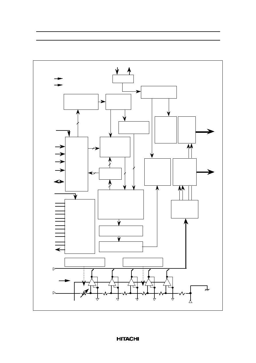
HD66750/1 Block Diagram
RS
RW/RD*
E/WR*
Vcc
V
LCD
16
12
16
Vci
C1+
IM1-0
C1-
+ -
+ -
+ -
+ -
VLOUT
+ -
GND
VR
R
R
R
0
R
R
V1OUT
V2OUT
V3OUT
V4OUT
V5OUT
OPOFF
DB0-DB15
VTEST
C2+
C2-
CS*
C3+
C3-
C4+
C4-
16
C5+
C5-
16
16
16
16
C6+
C6-
Instruction register
(IR)
Timing generator
CPG
Instruction
decoder
OSC1
OSC2
RESET*
TEST
System
interface
• 16-bit bus
• 8-bit bus
Address counter
(AC)
Graphic RAM
(CGRAM)
4,096 bytes
128-bit latch
circuit
128-bit
bidirectional
common shift
register
Common
driver
Segment
driver
LCD drive
voltage selector
COM1/128–
COM128/1
SEG1/128-
SEG128/1
Two-, five-,
six-, and
seven-times
booster
Contrast adjuster
Drive bias controller
Window cursor control
Four grayscale control
circuit
Read data
latch
Bit operation
• Chip size: 10.97 mm X 4.13 mm
• Pad coordinates: Pad center
• Coordinate origin: Chip center
• Au bump size: 40
µ
m x 90
µ
m
Chip corner bump size : 90
µ
m x 90
µ
m
(Dummy1, Dummy22, Dummy23 and Dummy 48)
• Au bump pitch: 60
µ
m (min.)
• Au bump height: 20
µ
m (typ.)
(Top view)
HD66750
Y
X
HD66750/1
HITACHI
9
HD66750 Pad Arrangement
COM29/100
COM28/101
COM27/102
COM26/103
COM25/104
COM24/105
COM23/106
COM22/107
COM21/108
COM20/109
COM19/110
COM18/111
COM17/112
COM119/10
COM118/11
COM117/12
COM116/13
COM115/14
COM114/15
COM113/16
SEG72/57
SEG128/1
SEG127/2
SEG126/3
SEG87/42
SEG88/41
SEG89/40
SEG125/4
SEG124/5
SEG123/6
SEG122/7
SEG121/8
SEG120/9
SEG119/10
SEG118/11
SEG117/12
SEG116/13
SEG115/14
SEG114/15
SEG113/16
SEG112/17
SEG111/18
SEG110/19
SEG109/20
SEG108/21
SEG107/22
SEG106/23
SEG105/24
SEG104/25
SEG103/26
SEG102/27
SEG101/28
SEG100/29
SEG99/30
SEG98/31
SEG97/32
SEG96/33
SEG95/34
SEG94/35
SEG93/36
SEG92/37
SEG91/38
SEG90/39
SEG86/43
SEG85/44
SEG84/45
SEG83/46
SEG82/47
SEG81/48
SEG80/49
SEG79/50
SEG78/51
SEG77/52
SEG76/53
SEG75/54
SEG74/55
SEG73/56
SEG71/58
SEG70/59
SEG69/60
SEG68/61
SEG67/62
SEG66/63
SEG65/64
SEG64/65
SEG63/66
SEG62/67
SEG61/68
SEG60/69
SEG59/70
SEG58/71
SEG57/72
SEG56/73
SEG55/74
SEG54/75
SEG53/76
SEG52/77
SEG51/78
SEG50/79
SEG49/80
SEG48/81
SEG47/82
SEG46/83
SEG45/84
SEG44/85
SEG43/86
SEG42/87
SEG41/88
SEG40/89
SEG39/90
SEG38/91
SEG37/92
SEG36/93
SEG35/94
SEG34/95
SEG33/96
SEG32/97
SEG31/98
SEG30/99
SEG29/100
SEG28/101
SEG27/102
SEG26/103
SEG25/104
SEG24/105
SEG23/106
SEG22/107
SEG21/108
SEG20/109
SEG19/110
SEG18/111
SEG17/112
SEG16/113
SEG15/114
SEG14/115
SEG13/116
SEG12/117
SEG11/118
SEG10/119
SEG9/120
SEG8/121
SEG7/122
SEG6/123
SEG5/124
SEG4/125
SEG3/126
SEG2/127
SEG1/128
COM64/65
COM63/66
COM62/67
COM61/68
COM60/69
COM59/70
COM58/71
COM57/72
COM56/73
COM55/74
COM54/75
COM53/76
COM52/77
COM51/78
COM50/79
COM49/80
COM48/81
COM47/82
COM46/83
COM45/84
COM44/85
COM43/86
COM42/87
COM41/88
COM40/89
COM39/90
COM38/91
COM37/92
COM36/93
COM35/94
COM34/95
COM33/96
COM32/97
COM31/98
COM30/99
COM16/113
COM15/114
COM14/115
COM13/116
COM12/117
COM11/118
COM10/119
COM9/120
COM8/121
COM7/122
COM6/123
COM5/124
COM4/125
COM3/126
COM2/127
COM1/128
COM128/1
COM127/2
COM126/3
COM125/4
COM124/5
COM123/6
COM122/7
COM121/8
COM120/9
COM112/17
COM111/18
COM110/19
COM109/20
COM108/21
COM107/22
COM106/23
COM105/24
COM72/57
COM71/58
COM70/59
COM69/60
COM68/61
COM67/62
COM66/63
COM65/64
COM87/42
COM88/41
COM89/40
COM104/25
COM103/26
COM102/27
COM101/28
COM100/29
COM99/30
COM98/31
COM97/32
COM96/33
COM95/34
COM94/35
COM93/36
COM92/37
COM91/38
COM90/39
COM86/43
COM85/44
COM84/45
COM83/46
COM82/47
COM81/48
COM80/49
COM79/50
COM78/51
COM77/52
COM76/53
COM75/54
COM74/55
COM73/56
OSC2
OSC1
E/WR*
RW/RD*
GND
RS
CS*
RESET*
DB0
DB1
DB2
DB3
DB4
DB5
DB6
DB7
GNDDUM1
IM1
IM0
VccDUM1
OPOFF
TEST
GNDDUM2
DB8
DB9
DB10
DB11
DB12
DB13
DB14
DB15
GNDDUM3
Dummy1
C1+
C2-
C2+
Vci
VTEST
C1-
VLOUT
V
LCD
Vcc
C3-
C3+
V1OUT
V2OUT
V3OUT
V4OUT
V5OUT
C4-
C4+
C5-
C5+
C6-
C6+
Dummy22
V
LCD
VLOUT
C1-
C1+
C2-
C2+
C3-
C3+
C4-
C4+
C5-
C5+
C6-
C6+
Vci
Vcc
GND
GND
GND
GND
RW/RD*
E/WR*
RS
CS*
RESET*
DB0
DB1
DB2
DB4
DB3
DB5
DB6
DB7
DB8
DB9
DB10
DB11
DB12
DB13
DB14
DB15
TEST
OPOFF
IM0
IM1
Dummy21
Dummy20
Dummy19
Dummy18
Dummy17
Dummy15
Dummy16
Dummy14
Dummy13
Dummy12
Dummy11
OSC1
OSC2
GND
GND
GND
GND
Dummy2
Dummy3
Dummy4
Dummy5
Dummy6
Dummy7
Dummy8
Dummy9
Dummy10
Dummy29
Dummy28
Dummy27
Dummy25
Dummy26
Dummy23
Dummy24
Dummy31
Dummy32
Dummy33
Dummy34
Dummy35
Dummy30
Dummy48
Dummy47
Dummy43
Dummy42
Dummy41
Dummy40
Dummy39
Dummy38
Dummy46
Dummy45
Dummy44
Dummy37
Dummy36
(note)
This figure is shown pad arrangement from chip top view
which has Au-bumps and LSI pattern layer.
OSC2
OSC1
E/WR*
RW/RD*
GND
RS
CS*
RESET*
DB0
DB1
DB2
DB3
DB4
DB5
DB6
DB7
GNDDUM1
IM1
IM0
VccDUM1
OPOFF
TEST
SEG128/1
SEG72/57
Dummy48
GNDDUM2
DB8
DB9
DB10
DB11
DB12
DB13
DB14
DB15
GNDDUM3
SEG127/2
SEG126/3
SEG87/42
Dummy1
SEG88/41
SEG89/40
C1+
C2-
C2+
Vci
VTEST
C1-
VLOUT
V
LCD
Vcc
C3-
C3+
V1OUT
V2OUT
V3OUT
V4OUT
V5OUT
C4-
C4+
C5-
C5+
C6-
C6+
SEG125/4
SEG124/5 SEG123/6
SEG122/7 SEG121/8
SEG120/9 SEG119/10
SEG118/11 SEG117/12
SEG116/13 SEG115/14
SEG114/15 SEG113/16
SEG112/17 SEG111/18
SEG110/19 SEG109/20
SEG108/21 SEG107/22
SEG106/23 SEG105/24
SEG104/25 SEG103/26
SEG102/27 SEG101/28
SEG100/29 SEG99/30
SEG98/31 SEG97/32
SEG96/33 SEG95/34
SEG94/35 SEG93/36
SEG92/37 SEG91/38
SEG90/39
SEG86/43 SEG85/44
SEG84/45 SEG83/46
SEG82/47 SEG81/48
SEG80/49 SEG79/50
SEG78/51 SEG77/52
SEG76/53 SEG75/54
SEG74/55 SEG73/56
SEG71/58
SEG70/59
SEG69/60
SEG68/61
SEG67/62
SEG66/63
SEG65/64
SEG64/65
SEG63/66
SEG62/67
SEG61/68
SEG60/69
SEG59/70
SEG58/71
SEG57/72
SEG56/73
SEG55/74
SEG54/75
SEG53/76
SEG52/77
SEG51/78
SEG50/79
SEG49/80
SEG48/81
SEG47/82
SEG46/83
SEG45/84
SEG44/85
SEG43/86
SEG42/87
SEG41/88
SEG40/89
SEG39/90
SEG38/91
SEG37/92
SEG36/93
SEG35/94
SEG34/95
SEG33/96
SEG32/97
SEG31/98
SEG30/99
SEG29/100
SEG28/101
SEG27/102
SEG26/103
SEG25/104
SEG24/105
SEG23/106
SEG22/107
SEG21/108
SEG20/109
SEG19/110
SEG18/111
SEG17/112
SEG16/113
SEG15/114
SEG14/115
SEG13/116
SEG12/117
SEG11/118
SEG10/119
SEG9/120
SEG8/121
SEG7/122
SEG6/123
SEG5/124
SEG4/125
SEG3/126
SEG2/127
SEG1/128
Dummy29
Dummy22
COM72/57
COM71/58
COM70/59
COM69/60
COM68/61
COM67/62
COM66/63
COM65/64
COM64/65
COM63/66
COM62/67
COM61/68
COM60/69
COM59/70
COM58/71
COM57/72
COM56/73
COM55/74
COM54/75
COM53/76
COM52/77
COM51/78
COM50/79
COM49/80
COM48/81
COM47/82
COM46/83
COM45/84
COM44/85
COM43/86
COM42/87
COM41/88
COM40/89
COM39/90
COM38/91
COM37/92
COM36/93
COM35/94
COM34/95
COM33/96
COM32/97
COM31/98
COM30/99
COM29/100
COM28/101
COM27/102
COM26/103
COM25/104
COM24/105
COM23/106
COM22/107
COM21/108
COM20/109
COM19/110
COM18/111
COM17/112
COM16/113
COM15/114
COM14/115
COM13/116
COM12/117
COM11/118
COM10/119
COM9/120
COM8/121
COM7/122
COM6/123
COM5/124
COM4/125
COM3/126
COM2/127
COM1/128
COM128/1
COM127/2
COM126/3
COM87/42
COM88/41
COM89/40
COM125/4
COM124/5
COM123/6
COM122/7
COM121/8
COM120/9
COM119/10
COM118/11
COM117/12
COM116/13
COM115/14
COM114/15
COM113/16
COM112/17
COM111/18
COM110/19
COM109/20
COM108/21
COM107/22
COM106/23
COM105/24
COM104/25
COM103/26
COM102/27
COM101/28
COM100/29
COM99/30
COM98/31
COM97/32
COM96/33
COM95/34
COM94/35
COM93/36
COM92/37
COM91/38
COM90/39
COM86/43
COM85/44
COM84/45
COM83/46
COM82/47
COM81/48
COM80/49
COM79/50
COM78/51
COM77/52
COM76/53
COM75/54
COM74/55
COM73/56
Dummy28
Dummy27
Dummy25
VLOUT
C1-
C1+
C2-
C2+
C3-
C3+
C4-
C4+
C5-
C5+
C6-
C6+
Vci
Vcc
GND
GND
GND
GND
RW/RD*
E/WR*
RS
CS*
RESET*
DB0
DB1
DB2
DB4
DB3
DB5
DB6
DB7
DB8
DB9
DB10
DB11
DB12
DB13
DB14
DB15
TEST
OPOFF
IM0
IM1
V
LCD
Dummy47
Dummy36
Dummy43
Dummy42
Dummy41
Dummy26
Dummy23
Dummy21
Dummy20
Dummy19
Dummy18
Dummy17
Dummy15
Dummy16
Dummy14
Dummy13
Dummy12
Dummy11
OSC1
OSC2
GND
GND
GND
GND
Dummy2
Dummy3
Dummy4
Dummy5
Dummy6
Dummy7
Dummy8
Dummy9
Dummy10
Dummy24
Dummy31
Dummy32
Dummy33
Dummy34
Dummy35
Dummy40
Dummy39
Dummy38
Dummy37
Dummy46
Dummy45
Dummy44
Dummy30
(Top view)
HD66751
Y
X
HD66750/1
HITACHI
10
HD66751 Pad Arrangement
• Chip size: 10.97 mm X 4.13 mm
• Pad coordinates: Pad center
• Coordinate origin: Chip center
• Au bump size: 40
µ
m x 90
µ
m
Chip corner bump size : 90
µ
m x 90
µ
m
(Dummy1, Dummy22, Dummy23 and Dummy 48)
• Au bump pitch: 60
µ
m (min.)
• Au bump height: 20
µ
m (typ.)
(note)
This figure is shown pad arrangement from chip top view
which has Au-bumps and LSI pattern layer.

HD66750/1
HD66750 Pad Coordinate
PAD NAME
X
Y
PAD NAME
X
Y
PAD NAME
X
Y
PAD NAME
X
Y
PAD NAME
X
Y
1 Dummy1
-5269
-1895
83 C6+
1582 -1849
165 COM54/75
5269
571
247 SEG43/86
1310
1849
329 SEG125/4
-3655
1849
2 Dummy2
-5089
-1895
84 C6-
1703 -1849
166 COM55/74
5269
631
248 SEG44/85
1250
1849
330 SEG126/3
-3715
1849
3 Dummy3
-5029
-1895
85 C6-
1763 -1849
167 COM56/73
5269
691
249 SEG45/84
1190
1849
331 SEG127/2
-3775
1849
4 Dummy4
-4969
-1895
86 C5+
1883 -1849
168 COM57/72
5269
752
250 SEG46/83
1130
1849
332 SEG128/1
-3835
1849
5 Dummy5
-4909
-1895
87 C5+
1943 -1849
169 COM58/71
5269
812
251 SEG47/82
1070
1849
333 COM112/17 -3931
1849
6 Dummy6
-4848
-1895
88 C5-
2063 -1849
170 COM59/70
5269
872
252 SEG48/81
1010
1849
334 COM111/18 -3991
1849
7 Dummy7
-4788
-1895
89 C5-
2124 -1849
171 COM60/69
5269
932
253 SEG49/80
950
1849
335 COM110/19 -4051
1849
8 Dummy8
-4728
-1895
90 C4+
2244 -1849
172 COM61/68
5269
992
254 SEG50/79
889
1849
336 COM109/20 -4111
1849
9 Dummy9
-4668
-1895
91 C4+
2304 -1849
173 COM62/67
5269
1052
255 SEG51/78
829
1849
337 COM108/21 -4171
1849
10 Dummy10
-4608
-1895
92 C4-
2424 -1849
174 COM63/66
5269
1112
256 SEG52/77
769
1849
338 COM107/22 -4232
1849
11 GNDDUM1
-4454
-1895
93 C4-
2484 -1849
175 COM64/65
5269
1172
257 SEG53/76
709
1849
339 COM106/23 -4292
1849
12 IM1
-4394
-1895
94 C3+
2605 -1849
176 COM113/16
5269
1232
258 SEG54/75
649
1849
340 COM105/24 -4352
1849
13 IM1
-4334
-1895
95 C3+
2665 -1849
177 COM114/15
5269
1293
259 SEG55/74
589
1849
341 Dummy36
-4428
1895
14 IM0
-4210
-1895
96 C3-
2785 -1849
178 COM115/14
5269
1353
260 SEG56/73
529
1849
342 Dummy37
-4488
1895
15 IM0
-4150
-1895
97 C3-
2845 -1849
179 COM116/13
5269
1413
261 SEG57/72
469
1849
343 Dummy38
-4548
1895
16 VccDUM1
-4086
-1895
98 C2+
2965 -1849
180 COM117/12
5269
1473
262 SEG58/71
409
1849
344 Dummy39
-4608
1895
17 OPOFF
-4026
-1895
99 C2+
3025 -1849
181 COM118/11
5269
1533
263 SEG59/70
348
1849
345 Dummy40
-4668
1895
18 OPOFF
-3966
-1895
100 C2-
3146 -1849
182 COM119/10
5269
1593
264 SEG60/69
288
1849
346 Dummy41
-4728
1895
19 TEST
-3842
-1895
101 C2-
3206 -1849
183 COM120/9
5269
1653
265 SEG61/68
228
1849
347 Dummy42
-4788
1895
20 TEST
-3782
-1895
102 C1+
3326 -1849
184 Dummy23
5269
1895
266 SEG62/67
168
1849
348 Dummy43
-4848
1895
21 GNDDUM2
-3722
-1895
103 C1+
3386 -1849
185 Dummy24
5089
1895
267 SEG63/66
108
1849
349 Dummy44
-4909
1895
22 DB15
-3658
-1895
104 C1-
3506 -1849
186 Dummy25
5029
1895
268 SEG64/65
48
1849
350 Dummy45
-4969
1895
23 DB15
-3598
-1895
105 C1-
3566 -1849
187 Dummy26
4969
1895
269 SEG65/64
-48
1849
351 Dummy46
-5029
1895
24 DB14
-3474
-1895
106 VLOUT
3687 -1849
188 Dummy27
4909
1895
270 SEG66/63
-108
1849
352 Dummy47
-5089
1895
25 DB14
-3414
-1895
107 VLOUT
3747 -1849
189 Dummy28
4848
1895
271 SEG67/62
-168
1849
353 Dummy48
-5269
1895
26 DB13
-3290
-1895
108 VLCD
3867 -1849
190 Dummy29
4788
1895
272 SEG68/61
-228
1849
354 COM104/25 -5269
1653
27 DB13
-3230
-1895
109 VLCD
3927 -1849
191 Dummy30
4728
1895
273 SEG69/60
-288
1849
355 COM103/26 -5269
1593
28 DB12
-3106
-1895
110 V1OUT
4047 -1849
192 Dummy31
4668
1895
274 SEG70/59
-348
1849
356 COM102/27 -5269
1533
29 DB12
-3046
-1895
111 V2OUT
4108 -1849
193 Dummy32
4608
1895
275 SEG71/58
-409
1849
357 COM101/28 -5269
1473
30 DB11
-2922
-1895
112 V3OUT
4168 -1849
194 Dummy33
4548
1895
276 SEG72/57
-469
1849
358 COM100/29 -5269
1413
31 DB11
-2862
-1895
113 V4OUT
4228 -1849
195 Dummy34
4488
1895
277 SEG73/56
-529
1849
359 COM99/30
-5269
1353
32 DB10
-2738
-1895
114 V5OUT
4288 -1849
196 Dummy35
4428
1895
278 SEG74/55
-589
1849
360 COM98/31
-5269
1293
33 DB10
-2678
-1895
115 VTEST
4348 -1849
197 COM121/8
4352
1849
279 SEG75/54
-649
1849
361 COM97/32
-5269
1232
34 DB9
-2554
-1895
116 Dummy11
4488 -1895
198 COM122/7
4292
1849
280 SEG76/53
-709
1849
362 COM96/33
-5269
1172
35 DB9
-2494
-1895
117 Dummy12
4548 -1895
199 COM123/6
4232
1849
281 SEG77/52
-769
1849
363 COM95/34
-5269
1112
36 DB8
-2370
-1895
118 Dummy13
4608 -1895
200 COM124/5
4171
1849
282 SEG78/51
-829
1849
364 COM94/35
-5269
1052
37 DB8
-2310
-1895
119 Dummy14
4668 -1895
201 COM125/4
4111
1849
283 SEG79/50
-889
1849
365 COM93/36
-5269
992
38 DB7
-2186
-1895
120 Dummy15
4728 -1895
202 COM126/3
4051
1849
284 SEG80/49
-950
1849
366 COM92/37
-5269
932
39 DB7
-2126
-1895
121 Dummy16
4788 -1895
203 COM127/2
3991
1849
285 SEG81/48
-1010
1849
367 COM91/38
-5269
872
40 DB6
-2002
-1895
122 Dummy17
4848 -1895
204 COM128/1
3931
1849
286 SEG82/47
-1070
1849
368 COM90/39
-5269
812
41 DB6
-1942
-1895
123 Dummy18
4909 -1895
205 SEG1/128
3835
1849
287 SEG83/46
-1130
1849
369 COM89/40
-5269
752
42 DB5
-1818
-1895
124 Dummy19
4969 -1895
206 SEG2/127
3775
1849
288 SEG84/45
-1190
1849
370 COM88/41
-5269
691
43 DB5
-1758
-1895
125 Dummy20
5029 -1895
207 SEG3/126
3715
1849
289 SEG85/44
-1250
1849
371 COM87/42
-5269
631
44 DB4
-1634
-1895
126 Dummy21
5089 -1895
208 SEG4/125
3655
1849
290 SEG86/43
-1310
1849
372 COM86/43
-5269
571
45 DB4
-1574
-1895
127 Dummy22
5269 -1895
209 SEG5/124
3595
1849
291 SEG87/42
-1370
1849
373 COM85/44
-5269
511
46 DB3
-1450
-1895
128 COM17/112
5269 -1653
210 SEG6/123
3535
1849
292 SEG88/41
-1431
1849
374 COM84/45
-5269
451
47 DB3
-1390
-1895
129 COM18/111
5269 -1593
211 SEG7/122
3475
1849
293 SEG89/40
-1491
1849
375 COM83/46
-5269
391
48 DB2
-1266
-1895
130 COM19/110
5269 -1533
212 SEG8/121
3415
1849
294 SEG90/39
-1551
1849
376 COM82/47
-5269
331
49 DB2
-1206
-1895
131 COM20/109
5269 -1473
213 SEG9/120
3354
1849
295 SEG91/38
-1611
1849
377 COM81/48
-5269
271
50 DB1
-1083
-1895
132 COM21/108
5269 -1413
214 SEG10/119
3294
1849
296 SEG92/37
-1671
1849
378 COM80/49
-5269
210
51 DB1
-1022
-1895
133 COM22/107
5269 -1353
215 SEG11/118
3234
1849
297 SEG93/36
-1731
1849
379 COM79/50
-5269
150
52 DB0
-899
-1895
134 COM23/106
5269 -1293
216 SEG12/117
3174
1849
298 SEG94/35
-1791
1849
380 COM78/51
-5269
90
53 DB0
-838
-1895
135 COM24/105
5269 -1232
217 SEG13/116
3114
1849
299 SEG95/34
-1851
1849
381 COM77/52
-5269
30
54 GNDDUM3
-775
-1895
136 COM25/104
5269 -1172
218 SEG14/115
3054
1849
300 SEG96/33
-1912
1849
382 COM76/53
-5269
-30
55 RESET*
-715
-1895
137 COM26/103
5269 -1112
219 SEG15/114
2994
1849
301 SEG97/32
-1972
1849
383 COM75/54
-5269
-90
56 RESET*
-654
-1895
138 COM27/102
5269 -1052
220 SEG16/113
2934
1849
302 SEG98/31
-2032
1849
384 COM74/55
-5269
-150
57 CS*
-531
-1895
139 COM28/101
5269
-992
221 SEG17/112
2873
1849
303 SEG99/30
-2092
1849
385 COM73/56
-5269
-210
58 CS*
-471
-1895
140 COM29/100
5269
-932
222 SEG18/111
2813
1849
304 SEG100/29
-2152
1849
386 COM72/57
-5269
-271
59 RS
-347
-1895
141 COM30/99
5269
-872
223 SEG19/110
2753
1849
305 SEG101/28
-2212
1849
387 COM71/58
-5269
-331
60 RS
-287
-1895
142 COM31/98
5269
-812
224 SEG20/109
2693
1849
306 SEG102/27
-2272
1849
388 COM70/59
-5269
-391
61 E/WR*
-163
-1895
143 COM32/97
5269
-752
225 SEG21/108
2633
1849
307 SEG103/26
-2332
1849
389 COM69/60
-5269
-451
62 E/WR*
-103
-1895
144 COM33/96
5269
-691
226 SEG22/107
2573
1849
308 SEG104/25
-2392
1849
390 COM68/61
-5269
-511
63 RW/RD*
21
-1895
145 COM34/95
5269
-631
227 SEG23/106
2513
1849
309 SEG105/24
-2453
1849
391 COM67/62
-5269
-571
64 RW/RD*
81
-1895
146 COM35/94
5269
-571
228 SEG24/105
2453
1849
310 SEG106/23
-2513
1849
392 COM66/63
-5269
-631
65 GND
151
-1895
147 COM36/93
5269
-511
229 SEG25/104
2392
1849
311 SEG107/22
-2573
1849
393 COM65/64
-5269
-691
66 GND
211
-1895
148 COM37/92
5269
-451
230 SEG26/103
2332
1849
312 SEG108/21
-2633
1849
394 COM16/113 -5269
-752
67 GND
271
-1895
149 COM38/91
5269
-391
231 SEG27/102
2272
1849
313 SEG109/20
-2693
1849
395 COM15/114 -5269
-812
68 GND
332
-1895
150 COM39/90
5269
-331
232 SEG28/101
2212
1849
314 SEG110/19
-2753
1849
396 COM14/115 -5269
-872
69 GND
392
-1895
151 COM40/89
5269
-271
233 SEG29/100
2152
1849
315 SEG111/18
-2813
1849
397 COM13/116 -5269
-932
70 GND
452
-1895
152 COM41/88
5269
-210
234 SEG30/99
2092
1849
316 SEG112/17
-2873
1849
398 COM12/117 -5269
-992
71 GND
512
-1895
153 COM42/87
5269
-150
235 SEG31/98
2032
1849
317 SEG113/16
-2934
1849
399 COM11/118 -5269 -1052
72 GND
572
-1895
154 COM43/86
5269
-90
236 SEG32/97
1972
1849
318 SEG114/15
-2994
1849
400 COM10/119 -5269 -1112
73 GND
632
-1895
155 COM44/85
5269
-30
237 SEG33/96
1912
1849
319 SEG115/14
-3054
1849
401 COM9/120
-5269 -1172
74 OSC2
702
-1895
156 COM45/84
5269
30
238 SEG34/95
1851
1849
320 SEG116/13
-3114
1849
402 COM8/121
-5269 -1232
75 OSC2
762
-1895
157 COM46/83
5269
90
239 SEG35/94
1791
1849
321 SEG117/12
-3174
1849
403 COM7/122
-5269 -1293
76 OSC1
886
-1895
158 COM47/82
5269
150
240 SEG36/93
1731
1849
322 SEG118/11
-3234
1849
404 COM6/123
-5269 -1353
77 OSC1
946
-1895
159 COM48/81
5269
210
241 SEG37/92
1671
1849
323 SEG119/10
-3294
1849
405 COM5/124
-5269 -1413
78 Vcc
1119
-1849
160 COM49/80
5269
271
242 SEG38/91
1611
1849
324 SEG120/9
-3354
1849
406 COM4/125
-5269 -1473
79 Vcc
1179
-1849
161 COM50/79
5269
331
243 SEG39/90
1551
1849
325 SEG121/8
-3415
1849
407 COM3/126
-5269 -1533
80 Vci
1342
-1849
162 COM51/78
5269
391
244 SEG40/89
1491
1849
326 SEG122/7
-3475
1849
408 COM2/127
-5269 -1593
81 Vci
1402
-1849
163 COM52/77
5269
451
245 SEG41/88
1431
1849
327 SEG123/6
-3535
1849
409 COM1/128
-5269 -1653
82 C6+
1522
-1849
164 COM53/76
5269
511
246 SEG42/87
1370
1849
328 SEG124/5
-3595
1849
11
HD66750/1
HD66751 Pad Coordinate
PAD NAME
X
Y
PAD NAME
X
Y
PAD NAME
X
Y
PAD NAME
X
Y
PAD NAME
X
Y
1 Dummy1
-5269
-1895
83 C6+
1582 -1849
165 COM38/91
5269
571
247 COM107/22
1310
1849
329 SEG61/68
-3655
1849
2 Dummy2
-5089
-1895
84 C6-
1703 -1849
166 COM39/90
5269
631
248 COM108/21
1250
1849
330 SEG62/67
-3715
1849
3 Dummy3
-5029
-1895
85 C6-
1763 -1849
167 COM40/89
5269
691
249 COM109/20
1190
1849
331 SEG63/66
-3775
1849
4 Dummy4
-4969
-1895
86 C5+
1883 -1849
168 COM41/88
5269
752
250 COM110/19
1130
1849
332 SEG64/65
-3835
1849
5 Dummy5
-4909
-1895
87 C5+
1943 -1849
169 COM42/87
5269
812
251 COM111/18
1070
1849
333 SEG65/64
-3931
1849
6 Dummy6
-4848
-1895
88 C5-
2063 -1849
170 COM43/86
5269
872
252 COM112/17
1010
1849
334 SEG66/63
-3991
1849
7 Dummy7
-4788
-1895
89 C5-
2124 -1849
171 COM44/85
5269
932
253 COM113/16
950
1849
335 SEG67/62
-4051
1849
8 Dummy8
-4728
-1895
90 C4+
2244 -1849
172 COM45/84
5269
992
254 COM114/15
889
1849
336 SEG68/61
-4111
1849
9 Dummy9
-4668
-1895
91 C4+
2304 -1849
173 COM46/83
5269
1052
255 COM115/14
829
1849
337 SEG69/60
-4171
1849
10 Dummy10
-4608
-1895
92 C4-
2424 -1849
174 COM47/82
5269
1112
256 COM116/13
769
1849
338 SEG70/59
-4232
1849
11 GNDDUM1
-4454
-1895
93 C4-
2484 -1849
175 COM48/81
5269
1172
257 COM117/12
709
1849
339 SEG71/58
-4292
1849
12 IM1
-4394
-1895
94 C3+
2605 -1849
176 COM49/80
5269
1232
258 COM118/11
649
1849
340 SEG72/57
-4352
1849
13 IM1
-4334
-1895
95 C3+
2665 -1849
177 COM50/79
5269
1293
259 COM119/10
589
1849
341 Dummy36
-4428
1895
14 IM0
-4210
-1895
96 C3-
2785 -1849
178 COM51/78
5269
1353
260 COM120/9
529
1849
342 Dummy37
-4488
1895
15 IM0
-4150
-1895
97 C3-
2845 -1849
179 COM52/77
5269
1413
261 COM121/8
469
1849
343 Dummy38
-4548
1895
16 VccDUM1
-4086
-1895
98 C2+
2965 -1849
180 COM53/76
5269
1473
262 COM122/7
409
1849
344 Dummy39
-4608
1895
17 OPOFF
-4026
-1895
99 C2+
3025 -1849
181 COM54/75
5269
1533
263 COM123/6
348
1849
345 Dummy40
-4668
1895
18 OPOFF
-3966
-1895
100 C2-
3146 -1849
182 COM55/74
5269
1593
264 COM124/5
288
1849
346 Dummy41
-4728
1895
19 TEST
-3842
-1895
101 C2-
3206 -1849
183 COM56/73
5269
1653
265 COM125/4
228
1849
347 Dummy42
-4788
1895
20 TEST
-3782
-1895
102 C1+
3326 -1849
184 Dummy23
5269
1895
266 COM126/3
168
1849
348 Dummy43
-4848
1895
21 GNDDUM2
-3722
-1895
103 C1+
3386 -1849
185 Dummy24
5089
1895
267 COM127/2
108
1849
349 Dummy44
-4909
1895
22 DB15
-3658
-1895
104 C1-
3506 -1849
186 Dummy25
5029
1895
268 COM128/1
48
1849
350 Dummy45
-4969
1895
23 DB15
-3598
-1895
105 C1-
3566 -1849
187 Dummy26
4969
1895
269 SEG1/128
-48
1849
351 Dummy46
-5029
1895
24 DB14
-3474
-1895
106 VLOUT
3687 -1849
188 Dummy27
4909
1895
270 SEG2/127
-108
1849
352 Dummy47
-5089
1895
25 DB14
-3414
-1895
107 VLOUT
3747 -1849
189 Dummy28
4848
1895
271 SEG3/126
-168
1849
353 Dummy48
-5269
1895
26 DB13
-3290
-1895
108 VLCD
3867 -1849
190 Dummy29
4788
1895
272 SEG4/125
-228
1849
354 SEG73/56
-5269
1653
27 DB13
-3230
-1895
109 VLCD
3927 -1849
191 Dummy30
4728
1895
273 SEG5/124
-288
1849
355 SEG74/55
-5269
1593
28 DB12
-3106
-1895
110 V1OUT
4047 -1849
192 Dummy31
4668
1895
274 SEG6/123
-348
1849
356 SEG75/54
-5269
1533
29 DB12
-3046
-1895
111 V2OUT
4108 -1849
193 Dummy32
4608
1895
275 SEG7/122
-409
1849
357 SEG76/53
-5269
1473
30 DB11
-2922
-1895
112 V3OUT
4168 -1849
194 Dummy33
4548
1895
276 SEG8/121
-469
1849
358 SEG77/52
-5269
1413
31 DB11
-2862
-1895
113 V4OUT
4228 -1849
195 Dummy34
4488
1895
277 SEG9/120
-529
1849
359 SEG78/51
-5269
1353
32 DB10
-2738
-1895
114 V5OUT
4288 -1849
196 Dummy35
4428
1895
278 SEG10/119
-589
1849
360 SEG79/50
-5269
1293
33 DB10
-2678
-1895
115 VTEST
4348 -1849
197 COM57/72
4352
1849
279 SEG11/118
-649
1849
361 SEG80/49
-5269
1232
34 DB9
-2554
-1895
116 Dummy11
4488 -1895
198 COM58/71
4292
1849
280 SEG12/117
-709
1849
362 SEG81/48
-5269
1172
35 DB9
-2494
-1895
117 Dummy12
4548 -1895
199 COM59/70
4232
1849
281 SEG13/116
-769
1849
363 SEG82/47
-5269
1112
36 DB8
-2370
-1895
118 Dummy13
4608 -1895
200 COM60/69
4171
1849
282 SEG14/115
-829
1849
364 SEG83/46
-5269
1052
37 DB8
-2310
-1895
119 Dummy14
4668 -1895
201 COM61/68
4111
1849
283 SEG15/114
-889
1849
365 SEG84/45
-5269
992
38 DB7
-2186
-1895
120 Dummy15
4728 -1895
202 COM62/67
4051
1849
284 SEG16/113
-950
1849
366 SEG85/44
-5269
932
39 DB7
-2126
-1895
121 Dummy16
4788 -1895
203 COM63/66
3991
1849
285 SEG17/112
-1010
1849
367 SEG86/43
-5269
872
40 DB6
-2002
-1895
122 Dummy17
4848 -1895
204 COM64/65
3931
1849
286 SEG18/111
-1070
1849
368 SEG87/42
-5269
812
41 DB6
-1942
-1895
123 Dummy18
4909 -1895
205 COM65/64
3835
1849
287 SEG19/110
-1130
1849
369 SEG88/41
-5269
752
42 DB5
-1818
-1895
124 Dummy19
4969 -1895
206 COM66/63
3775
1849
288 SEG20/109
-1190
1849
370 SEG89/40
-5269
691
43 DB5
-1758
-1895
125 Dummy20
5029 -1895
207 COM67/62
3715
1849
289 SEG21/108
-1250
1849
371 SEG90/39
-5269
631
44 DB4
-1634
-1895
126 Dummy21
5089 -1895
208 COM68/61
3655
1849
290 SEG22/107
-1310
1849
372 SEG91/38
-5269
571
45 DB4
-1574
-1895
127 Dummy22
5269 -1895
209 COM69/60
3595
1849
291 SEG23/106
-1370
1849
373 SEG92/37
-5269
511
46 DB3
-1450
-1895
128 COM1/128
5269 -1653
210 COM70/59
3535
1849
292 SEG24/105
-1431
1849
374 SEG93/36
-5269
451
47 DB3
-1390
-1895
129 COM2/127
5269 -1593
211 COM71/58
3475
1849
293 SEG25/104
-1491
1849
375 SEG94/35
-5269
391
48 DB2
-1266
-1895
130 COM3/126
5269 -1533
212 COM72/57
3415
1849
294 SEG26/103
-1551
1849
376 SEG95/34
-5269
331
49 DB2
-1206
-1895
131 COM4/125
5269 -1473
213 COM73/56
3354
1849
295 SEG27/102
-1611
1849
377 SEG96/33
-5269
271
50 DB1
-1083
-1895
132 COM5/124
5269 -1413
214 COM74/55
3294
1849
296 SEG28/101
-1671
1849
378 SEG97/32
-5269
210
51 DB1
-1022
-1895
133 COM6/123
5269 -1353
215 COM75/54
3234
1849
297 SEG29/100
-1731
1849
379 SEG98/31
-5269
150
52 DB0
-899
-1895
134 COM7/122
5269 -1293
216 COM76/53
3174
1849
298 SEG30/99
-1791
1849
380 SEG99/30
-5269
90
53 DB0
-838
-1895
135 COM8/121
5269 -1232
217 COM77/52
3114
1849
299 SEG31/98
-1851
1849
381 SEG100/29
-5269
30
54 GNDDUM3
-775
-1895
136 COM9/120
5269 -1172
218 COM78/51
3054
1849
300 SEG32/97
-1912
1849
382 SEG101/28
-5269
-30
55 RESET*
-715
-1895
137 COM10/119
5269 -1112
219 COM79/50
2994
1849
301 SEG33/96
-1972
1849
383 SEG102/27
-5269
-90
56 RESET*
-654
-1895
138 COM11/118
5269 -1052
220 COM80/49
2934
1849
302 SEG34/95
-2032
1849
384 SEG103/26
-5269
-150
57 CS*
-531
-1895
139 COM12/117
5269
-992
221 COM81/48
2873
1849
303 SEG35/94
-2092
1849
385 SEG104/25
-5269
-210
58 CS*
-471
-1895
140 COM13/116
5269
-932
222 COM82/47
2813
1849
304 SEG36/93
-2152
1849
386 SEG105/24
-5269
-271
59 RS
-347
-1895
141 COM14/115
5269
-872
223 COM83/46
2753
1849
305 SEG37/92
-2212
1849
387 SEG106/23
-5269
-331
60 RS
-287
-1895
142 COM15/114
5269
-812
224 COM84/45
2693
1849
306 SEG38/91
-2272
1849
388 SEG107/22
-5269
-391
61 E/WR*
-163
-1895
143 COM16/113
5269
-752
225 COM85/44
2633
1849
307 SEG39/90
-2332
1849
389 SEG108/21
-5269
-451
62 E/WR*
-103
-1895
144 COM17/112
5269
-691
226 COM86/43
2573
1849
308 SEG40/89
-2392
1849
390 SEG109/20
-5269
-511
63 RW/RD*
21
-1895
145 COM18/111
5269
-631
227 COM87/42
2513
1849
309 SEG41/88
-2453
1849
391 SEG110/19
-5269
-571
64 RW/RD*
81
-1895
146 COM19/110
5269
-571
228 COM88/41
2453
1849
310 SEG42/87
-2513
1849
392 SEG111/18
-5269
-631
65 GND
151
-1895
147 COM20/109
5269
-511
229 COM89/40
2392
1849
311 SEG43/86
-2573
1849
393 SEG112/17
-5269
-691
66 GND
211
-1895
148 COM21/108
5269
-451
230 COM90/39
2332
1849
312 SEG44/85
-2633
1849
394 SEG113/16
-5269
-752
67 GND
271
-1895
149 COM22/107
5269
-391
231 COM91/38
2272
1849
313 SEG45/84
-2693
1849
395 SEG114/15
-5269
-812
68 GND
332
-1895
150 COM23/106
5269
-331
232 COM92/37
2212
1849
314 SEG46/83
-2753
1849
396 SEG115/14
-5269
-872
69 GND
392
-1895
151 COM24/105
5269
-271
233 COM93/36
2152
1849
315 SEG47/82
-2813
1849
397 SEG116/13
-5269
-932
70 GND
452
-1895
152 COM25/104
5269
-210
234 COM94/35
2092
1849
316 SEG48/81
-2873
1849
398 SEG117/12
-5269
-992
71 GND
512
-1895
153 COM26/103
5269
-150
235 COM95/34
2032
1849
317 SEG49/80
-2934
1849
399 SEG118/11
-5269 -1052
72 GND
572
-1895
154 COM27/102
5269
-90
236 COM96/33
1972
1849
318 SEG50/79
-2994
1849
400 SEG119/10
-5269 -1112
73 GND
632
-1895
155 COM28/101
5269
-30
237 COM97/32
1912
1849
319 SEG51/78
-3054
1849
401 SEG120/9
-5269 -1172
74 OSC2
702
-1895
156 COM29/100
5269
30
238 COM98/31
1851
1849
320 SEG52/77
-3114
1849
402 SEG121/8
-5269 -1232
75 OSC2
762
-1895
157 COM30/99
5269
90
239 COM99/30
1791
1849
321 SEG53/76
-3174
1849
403 SEG122/7
-5269 -1293
76 OSC1
886
-1895
158 COM31/98
5269
150
240 COM100/29
1731
1849
322 SEG54/75
-3234
1849
404 SEG123/6
-5269 -1353
77 OSC1
946
-1895
159 COM32/97
5269
210
241 COM101/28
1671
1849
323 SEG55/74
-3294
1849
405 SEG124/5
-5269 -1413
78 Vcc
1119
-1849
160 COM33/96
5269
271
242 COM102/27
1611
1849
324 SEG56/73
-3354
1849
406 SEG125/4
-5269 -1473
79 Vcc
1179
-1849
161 COM34/95
5269
331
243 COM103/26
1551
1849
325 SEG57/72
-3415
1849
407 SEG126/3
-5269 -1533
80 Vci
1342
-1849
162 COM35/94
5269
391
244 COM104/25
1491
1849
326 SEG58/71
-3475
1849
408 SEG127/2
-5269 -1593
81 Vci
1402
-1849
163 COM36/93
5269
451
245 COM105/24
1431
1849
327 SEG59/70
-3535
1849
409 SEG128/1
-5269 -1653
82 C6+
1522
-1849
164 COM37/92
5269
511
246 COM106/23
1370
1849
328 SEG60/69
-3595
1849
12
HD66750/1
13
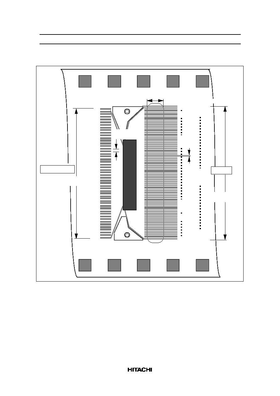
TCP Dimensions (HD66750TB0)
(SEG126/3)
(COM128/1)
SEG127/2
Bending slit
4.0 mm
COM1/128
COM16/113
SEG128/1
SEG1/128
COM17/112
0.14-mm
pitch
H
H
I
I
T
T
A
A
C
C
H
H
I
I
H
H
D
D
6
6
6
6
7
7
5
5
0
0
COM65/64
COM104/25
IM1
IM0
OPOFF
TEST
DB7
DB6
DB5
DB4
DB3
DB2
DB1
DB0
RESET*
CS*
RS
E/WR*
RW/RD*
GND
OSC2
OSC1
Vcc
Vci
C2+
C2-
C1+
C1-
VLOUT
VLCD
V1OUT
V2OUT
V3OUT
V4OUT
V5OUT
VTEST
0.65-mm
pitch
Dummy
Dummy
C3+
C3-
COM128/1
COM113/16
COM64/65
SEG126/3
SEG125/4
SEG2/127
SEG3/126
SEG4/125
C4+
C4-
DB8
DB9
DB10
DB11
DB12
DB13
DB14
DB15
C5+
C5-
C6+
C6-
(SEG128/1)
(SEG1/128)
(COM1/128)
(Dummy)
(Dummy)
(SEG127/2
(SEG125/4)
(SEG2/127)
(SEG3/126)
(SEG4/125)
(COM127/2)
(COM126/3)
(COM2/127)
(COM3/126)
HD66750
(HD66751)
I/O, Power supply
0.65P x (50 - 1)
= 31.85 mm
LCD drive
0.12P x (258 - 1)
= 30.784 mm

HD66750/1
14
Pin Functions
Table 2
Pin Functional Description
Signals
Number of
Pins
I/O
Connected to
Functions
IM1, IM0
2
I
GND or V
CC
Selects the MPU interface mode:
IM1
GND
GND
Vcc
Vcc
IM0
GND
Vcc
GND
Vcc
MPU interface mode
68-system 16-bit bus interface
68-system 8-bit bus interface
80-system 16-bit bus interface
80-system 8-bit bus interface
CS*
1
I
MPU
Selects the HD66750/1:
Low: HD66750/1 is selected and can be accessed
High: HD66750/1 is not selected and cannot be
accessed
Must be fixed at GND level when not in use.
RS
1
I
MPU
Selects the register.
Low: Index/status High: Control
E/WR*
1
I
MPU
For a 68-system bus interface, serves as an enable
signal to activate data read/write operation.
For an 80-system bus interface, serves as a write
strobe signal and writes data at the low level.
RW/RD*
1
I
MPU
For a 68-system bus interface, serves as a signal to
select data read/write operation.
Low: Write High: Read
For an 80-system bus interface, serves as a read
strobe signal and reads data at the low level.
DB0–DB15
16
I/O
MPU
Serves as a 16-bit bidirectional data bus.
For an 8-bit bus interface, data transfer uses DB15-
DB8; fix unused DB7-DB0 to the Vcc or GND level.
COM1/128–
COM128/1
128
O
LCD
Output signals for common drive: All the unused pins
output unselected waveforms. In the display-off
period (D = 0), sleep mode (SLP = 1), or standby
mode (STB = 1), all pins output GND level.
The CMS bit can change the shift direction of the
common signal. For example, if CMS = 0, COM1/128
is COM1, and COM128/1 is COM128. If CMS = 1,
COM1/128 is COM128, and COM128/1 is COM1.
Note that the start position of the common output is
shifted by CN1–CN0 bits.
SEG1/128–
SEG128/1
128
O
LCD
Output signals for segment drive. In the display-off
period (D = 0), sleep mode (SLP = 1), or standby
mode (STB = 1), all pins output GND level.
The SGS bit can change the shift direction of the
segment signal. For example, if SGS = 0, SEG1/128
is SEG1. If SGS = 1, SEG1/128 is SEG128.

HD66750/1
15
Table 2
Pin Functional Description (cont)
Signals
Number
of Pins
I/O
Connected
to
Functions
V1OUT≠
V5OUT
5
I or O
Open or
external
bleeder-resistor
Used for output from the internal operational
amplifiers when they are used (OPOFF = GND); attach
a capacitor to stabilize the output. When the
amplifiers are not used (OPOFF = V
CC
), V1 to V5
voltages can be supplied to these pins externally.
V
LCD
1
--
Power supply
Power supply for LCD drive. V
LCD
≠
GND = 17 V max.
V
CC
, GND
2
--
Power supply
V
CC
: +1.8 V to +5.5 V; GND (logic): 0 V
OSC1,
OSC2
2
I or O
Oscillation-
resistor or clock
For R-C oscillation using an external resistor, connect
an external resistor. For external clock supply, input
clock pulses to OSC1.
Vci
1
I
Power supply
Inputs a reference voltage and supplies power to the
booster; generates the liquid crystal display drive
voltage from the operating voltage. The boosting
output voltage must not be larger than the absolute
maximum ratings.
Must be left disconnected when the booster is not
used.
VLOUT
1
O
V
LCD
pin/booster
capacitance
Potential difference between Vci and GND is two- to
seven-times-boosted and then output. Magnitude of
boost is selected by instruction.
C1+, C1≠
2
--
Booster
capacitance
External capacitance should be connected here for
boosting.
C2+, C2≠
2
--
Booster
capacitance
External capacitance should be connected here for
boosting.
C3+, C3≠
2
--
Booster
capacitance
External capacitance should be connected here for
boosting.
C4+, C4≠
2
--
Booster
capacitance
External capacitance should be connected here for
boosting.
C5+, C5≠
2
--
Booster
capacitance
External capacitance should be connected here for
boosting.
C6+, C6≠
2
--
Booster
capacitance
External capacitance should be connected here for
boosting.
RESET*
1
I
MPU or external
R-C circuit
Reset pin. Initializes the LSI when low. Must be reset
after power-on.
OPOFF
1
I
V
CC
or GND
Turns the internal operational amplifier off when
OPOFF = V
CC
, and turns it on when OPOFF = GND. If
the amplifier is turned off (OPOFF = V
CC
), V1 to V5
must be supplied to the V1OUT to V5OUT pins.
VccDUM
2
O
Input pins
Outputs the internal V
CC
level; shorting this pin sets the
adjacent input pin to the V
CC
level.
GNDDUM
4
O
Input pins
Outputs the internal GND level; shorting this pin sets
the adjacent input pin to the GND level.
Dummy
4
--
--
Dummy pad. Must be left disconnected.
TEST
1
I
GND
Test pin. Must be fixed at GND level.
VTEST
1
--
--
Test pin. Must be left disconnected.

HD66750/1
16
Block Function Description
System Interface
The HD66750/1 has four high-speed system interfaces: an 80-system 16-bit/8-bit bus and a 68-system 16-
bit/8-bit bus. The interface mode is selected by the IM1-0 pins.
The HD66750/1 has three 16-bit registers: an index register (IR), a write data register (WDR), and a read
data register (RDR). The IR stores index information from the control registers and the CGRAM. The WDR
temporarily stores data to be written into control registers and the CGRAM, and the RDR temporarily stores
data read from the CGRAM. Data written into the CGRAM from the MPU is first written into the WDR and
then is automatically written into the CGRAM by internal operation. Data is read through the RDR when
reading from the CGRAM, and the first read data is invalid and the second and the following data are
normal. When a logic operation is performed inside of the HD66750/1 by using the display data set in the
CGRAM and the data written from the MPU, the data read through the RDR is used. Accordingly, the MPU
does not need to read data twice nor to fetch the read data into the MPU. This enables high-speed
processing.
Execution time for instruction excluding oscillation start is 0 clock cycle and instructions can be written in
succession.
Table 3
Register Selection by RS and R/W Bits
R/W Bits
RS Bits
Operations
0
0
Writes indexes into IR
1
0
Disabled
0
1
Writes into control registers and CGRAM through WDR
1
1
Reads from CGRAM through RDR
Bit Operation
The HD66750/1 supports the following functions: a bit rotation function that writes the data written from
the MPU into the CGRAM by moving the display position in bit units, a write data mask function that
selects and writes data into the CGRAM in bit units, and a logic operation function that performs logic
operations on the display data set in the CGRAM and writes into the CGRAM. With the 16-bit bus
interface, these functions can greatly reduce the processing loads of the MPU graphics software and can
rewrite the display data in the CGRAM at high speed. For details, see the Graphics Operation Function
section.
Address Counter (AC)
The address counter (AC) assigns addresses to the CGRAM. When an address set instruction is written into
the IR, the address information is sent from the IR to the AC.
After writing into the CGRAM, the AC is automatically incremented by 1 (or decremented by 1). After
reading from the data, the RDM bit automatically updates or does not update the AC.

HD66750/1
17
Graphic RAM (CGRAM)
The graphic RAM (CGRAM) stores bit-pattern data of 128 x 120 dots. It has two bits/pixel and 4096-byte
capacity.
Grayscale Control Circuit
The grayscale control circuit performs four-grayscale control with the frame rate control (FRC) method for
four-monochrome grayscale display. For details, see the Four Grayscale Display Function section.
Timing Generator
The timing generator generates timing signals for the operation of internal circuits such as the CGRAM.
The RAM read timing for display and internal operation timing by MPU access are generated separately to
avoid interference with one another.
Oscillation Circuit (OSC)
The HD66750/1 can provide R-C oscillation simply through the addition of an external oscillation-resistor
between the OSC1 and OSC2 pins. The appropriate oscillation frequency for operating voltage, display
size, and frame frequency can be obtained by adjusting the external-resistor value. Clock pulses can also be
supplied externally. Since R-C oscillation stops during the standby mode, current consumption can be
reduced. For details, see the Oscillation Circuit section.
Liquid Crystal Display Driver Circuit
The liquid crystal display driver circuit consists of 128 common signal drivers (COM1 to COM128) and
128 segment signal drivers (SEG1 to SEG128). When the number of lines are selected by a program, the
required common signal drivers automatically output drive waveforms, while the other common signal
drivers continue to output unselected waveforms.
Display pattern data is latched when 128-bit data has arrived. The latched data then enables the segment
signal drivers to generate drive waveform outputs. The shift direction of 128-bit data can be changed by
the SGS bit. The shift direction for the common driver can also be changed by the CMS bit by selecting an
appropriate direction for the device mounting configuration.
When multiplexing drive is not used, or during the standby or sleep mode, all the above common and
segment signal drivers output the GND level, halting the display.
Booster (DC-DC Converter)
The booster generates two-, five-, six-, or seven-times voltage input to the Vci pin. With this, both the
internal logic units and LCD drivers can be controlled with a single power supply. Boost output level from
twice to seven-times boost can be selected by software. For details, see the Power Supply for Liquid
Crystal Display Drive section.

HD66750/1
18
V-Pin Voltage Follower
A voltage follower for each voltage level (V1 to V5) reduces current consumption by the LCD drive power
supply circuit. No external resistors are required because of the internal bleeder-resistor, which generates
different levels of LCD drive voltage. This internal bleeder-resistor can be software-specified from 1/4 bias
to 1/11 bias, according to the liquid crystal display drive duty value. The voltage followers can be turned
off while multiplexing drive is not being used. For details, see the Power Supply for Liquid Crystal
Display Drive section.
Contrast Adjuster
The contrast adjuster can be used to adjust LCD contrast in 64 steps by varying the LCD drive voltage by
software. This can be used to select an appropriate LCD brightness or to compensate for temperature.
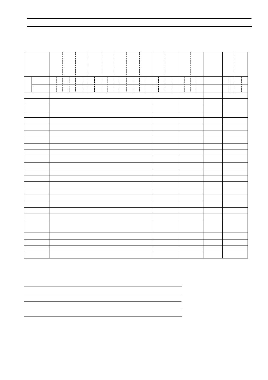
"001"H
"011"H
"021"H
"031"H
"041"H
"051"H
"061"H
"071"H
"081"H
"091"H
"0A1"H
"0B1"H
"0C1"H
"0D1"H
"0E1"H
"0F1"H
"101"H
"111"H
"121"H
"131"H
"7C1"H
"7D1"H
"7E1"H
"7F1"H
Table 4 Relationship between Display Position and CGRAM Address
HD66750/1
CGRAM Address Map
Note:
Upper bits: DB15, DB13, DB11, DB9, DB7, DB5, DB3, DB1
Lower bits: DB14, DB12, DB10, DB8, DB6, DB4, DB2, DB0
HITACHI
19
Table 5 Relationship between CGRAM Data and Display Contents
COM1
D0
D1
D2
D3
D4
D5
D6
D7
D8
D9 D10 D11 D12 D13 D14 D15 D0
SEG1/128
SEG2/127
SEG3/126
SEG4/125
SEG5/124
SEG6/123
SEG7/122
SEG8/121
SEG9/120
Segment
Driver
Bit
SGS="0"
SGS="1"
D15 D14 D13 D12 D11 D10 D9
D8
D7
D6 D5
D4
D3
D2
D1
D0 D15
D1
D14
D15
SEG16/113
D0
D0
SEG17/112
D15
D1
D14
D15
SEG24/105
D0
D0
SEG121/8
D15
D1
D14
D15
SEG128/1
D0
COM2
COM3
COM4
COM5
COM6
COM7
COM8
COM9
COM10
COM11
COM12
COM13
COM14
COM15
COM16
COM17
COM18
COM19
COM20
COM126
COM127
COM128
COM125
Address: "000"H
Address: "010"H
Address: "020"H
Address: "030"H
Address: "040"H
Address: "050"H
Address: "060"H
Address: "070"H
Address: "080"H
Address: "090"H
Address: "0A0"H
Address: "0B0"H
Address: "0C0"H
Address: "0D0"H
Address: "0E0"H
Address: "0F0"H
Address: "100"H
Address: "110"H
Address: "120"H
Address: "130"H
Address: "7C0"H
Address: "7D0"H
Address: "7E0"H
Address: "7F0"H
"002"H
"012"H
"022"H
"032"H
"042"H
"052"H
"062"H
"072"H
"082"H
"092"H
"0A2"H
"0B2"H
"0C2"H
"0D2"H
"0E2"H
"0F2"H
"102"H
"112"H
"122"H
"132"H
"7C2"H
"7D2"H
"7E2"H
"7F2"H
"00F"H
"01F"H
"02F"H
"03F"H
"04F"H
"05F"H
"06F"H
"07F"H
"08F"H
"09F"H
"0AF"H
"0BF"H
"0CF"H
"0DF"H
"0EF"H
"0FF"H
"10F"H
"11F"H
"12F"H
"13F"H
"7CF"H
"7DF"H
"7EF"H
"7FF"H
0
0
0
1
1
0
1
1
Non-selection display (unlit)
1/3- or 1/2-level grayscale display (selected by the GS bit)
2/3-level grayscale display
Selection display (lit)
Upper Bit
Lower Bit
LCD
•••
•••
••••••••••
•••
•••
•••
••••••••••
•••
•••
•••
••••••••••
•••
••••••••••
••••••••••
••••••••••
••••••••••
••••••••••
••••••••••
••••••••••
••••••••••
••••••••••
••••••••••
••••••••••
••••••••••
••••••••••
••••••••••
••••••••••
••••••••••
••••••••••
••••••••••
••••••••••
••••••••••
••••••••••
••••••••••
••••••••••
••••••••••
••••••••••
•
•
•
•
•
•
•
•
•
•
•
•
•
•
•

HD66750/1
20
Instructions
Outline
The HD66750/1 uses the 16-bit bus architecture. Before the internal operation of the HD66750/1 starts,
control information is temporarily stored in the registers described below to allow high-speed interfacing
with a high-performance microcomputer. The internal operation of the HD66750/1 is determined by
signals sent from the microcomputer. These signals, which include the register selection signal (RS), the
read/write signal (R/W), and the data bus signals (DB15 to DB7), make up the HD66750/1 instructions.
There are seven categories of instructions that:
•
Specify the index
•
Read the status
•
Control the display
•
Control power management
•
Process the graphics data
•
Set internal CGRAM addresses
•
Transfer data to and from the internal CGRAM
Normally, instructions that write data are used the most. However, an auto-update of internal CGRAM
addresses after each data write can lighten the microcomputer program load.
Because instructions are executed in 0 cycles, they can be written in succession.
HD66750/1
21
Instruction Descriptions
Index
The index instruction specifies the RAM control indexes (R00 to R12). It sets the register number in the
range of 00000 to 10010 in biniary form.
0
0
*
*
*
*
*
*
*
*
*
ID4
ID3
ID2 ID1
ID0
R/W
RS
DB7
DB0
DB6 DB5
DB4 DB3
DB2
DB1
DB8
DB9
DB10
DB11
DB12
DB13
DB14
DB15
*
*
Figure 1 Index Instruction
Status Read
The status read instruction reads the internal status of the HD66750/1.
L6–0: Indicate the driving raster-row position where the liquid crystal display is being driven.
C5–0: Read the contrast setting values (CT5–0).
1
0
L6
L5
L4
L3
L2
L1
L0
0
0
C5
C4
C3
C2
C1
C0
R/W
RS
DB7
DB0
DB6 DB5
DB4 DB3
DB2
DB1
DB8
DB9
DB10
DB11
DB12
DB13
DB14
DB15
0
Figure 2 Status Read Instruction
Start Oscillation
The start oscillation instruction restarts the oscillator from the halt state in the standby mode. After issuing
this instruction, wait at least 10 ms for oscillation to stabilize before issuing the next instruction. (See the
Standby Mode section.)
If this register is read forcibly when R/W = 1, 0750H is read.
0
1
*
*
*
*
*
*
*
1
R/W
RS
DB7
DB0
DB6 DB5
DB4 DB3
DB2
DB1
DB8
DB9
DB10
DB11
DB12
DB13
DB14
DB15
*
*
*
*
*
*
*
*
1
1
0
0
0
0
1
0
1
0
1
1
1
0
0
0
0
0
Figure 3 Start Oscillation Instruction

HD66750/1
22
Driver Output Control
CMS: Selects the output shift direction of a common driver. When CMS = 0, COM1/128 shifts to COM1,
and COM128/1 to COM128. When CMS = 1, COM1/128 shifts to COM128, and COM128/1 to COM1.
Output position of a common driver shifts depending on the CN bit setting.
SGS: Selects the output shift direction of a segment driver. When SGS = 0, SEG1/128 shifts to SEG1, and
SEG128/1 to SEG128. When SGS = 1, SEG1/128 shifts to SEG128, and SEG128/1 to SEG1.
CN: When CN = 1, the display position is shifted down by 32 raster-rows and display starts from COM33.
When the liquid crystal is driven at a low duty ratio in the system wait state, it can be partially displayed at
the center of the screen. For details, see the Partial-display-on Function section.
NL3-0: Specify the LCD drive duty ratio. The duty ratio can be adjusted for every eight raster-rows.
CGRAM address mapping does not depend on the setting value of the drive duty ratio.
0
1
CMS SGS
R/W
RS
DB7
DB0
DB6 DB5
DB4 DB3
DB2
DB1
DB8
DB9
DB10
DB11
DB12
DB13
DB14
DB15
NL0
NL1
NL2
NL3
CN
*
*
*
*
*
*
*
*
*
Figure 4 Driver Output Control Instruction
Table 6
NL Bits and Drive Duty
NL3
NL2
NL1
NL0
Display Size
LCD Drive Duty
Common Driver Used
0
0
0
0
128 x 8 dots
1/8 Duty
COM1–COM8
0
0
0
1
128 x 16 dots
1/16 Duty
COM1–COM16
0
0
1
0
128 x 24 dots
1/24 Duty
COM1–COM24
0
0
1
1
128 x 32 dots
1/32 Duty
COM1–COM32
0
1
0
0
128 x 40 dots
1/40 Duty
COM1–COM40
0
1
0
1
128 x 48 dots
1/48 Duty
COM1–COM48
0
1
1
0
128 x 56 dots
1/56 Duty
COM1–COM56
0
1
1
1
128 x 64 dots
1/64 Duty
COM1–COM64
1
0
0
0
128 x 72 dots
1/72 Duty
COM1–COM72
1
0
0
1
128 x 80 dots
1/80 Duty
COM1–COM80
1
0
1
0
128 x 88 dots
1/88 Duty
COM1–COM88
1
0
1
1
128 x 96 dots
1/96 Duty
COM1–COM96
1
1
0
0
128 x 104 dots
1/104 Duty
COM1–COM104
1
1
0
1
128 x 112 dots
1/112 Duty
COM1–COM112
1
1
1
0
128 x 120 dots
1/120 Duty
COM1–COM120
1
1
1
1
128 x 128 dots
1/128 Duty
COM1–COM128
HD66750/1
23
LCD-Driving-Waveform Control
B/C: When B/C = 0, a B-pattern waveform is generated and alternates in every frame for LCD drive. When
B/C = 1, a C-pattern waveform is generated and alternates in each raster-row specified by bits EOR and
NW4–NW0 in the LCD-driving-waveform control register. For details, see the n-raster-row Reversed AC
Drive section.
EOR: When the C-pattern waveform is set (B/C = 1) and EOR = 1, the odd/even frame-select signals and
the n-raster-row reversed signals are EORed for alternating drive. EOR is used when the LCD is not
alternated by combining the set values of the LCD drive duty ratio and the n raster-row. For details, see the
n-raster-row Reversed AC Drive section.
NW4–0: Specify the number of raster-rows n that will alternate at the C-pattern waveform setting (B/C =
1). NW4–NW0 alternate for every set value + 1 raster-row, and the first to the 32nd raster-rows can be
selected.
0
1
NW1 NW0
R/W
RS
DB7
DB0
DB6
DB5
DB4 DB3
DB2
DB1
DB8
DB9
DB10
DB11
DB12
DB13
DB14
DB15
NW2
NW3
NW4
EOR
*
B/C
*
*
*
*
*
*
*
*
Figure 5 LCD-Driving-Waveform Control Instruction

HD66750/1
24
Table 7
Common Driver Pin Function
Common Driver Pin Function
CN = 0 (Normal Output)
CN = 1 (Center Output)
Common
Driver Pin
CMS = 0
CMS = 1
CMS = 0
CMS = 1
COM1/128
COM1
COM128
COM97
COM96
•
•
•
•
•
•
•
•
•
•
COM8/121
COM8
COM121
COM104
COM89
COM9/120
COM9
COM120
COM105
COM88
•
•
•
•
•
•
•
•
•
•
COM16/113
COM16
COM113
COM112
COM81
COM17/112
COM17
COM112
COM113
COM80
•
•
•
•
•
•
•
•
•
•
COM24/105
COM24
COM105
COM120
COM73
COM25/104
COM25
COM104
(COM121)
COM72
•
•
•
•
•
•
•
•
•
•
COM32/97
COM32
COM97
(COM128)
COM65
COM33/96
COM33
COM96
COM1
COM64
•
•
•
•
•
•
•
•
•
•
COM40/89
COM40
COM89
COM8
COM57
COM41/88
COM41
COM88
COM9
COM56
•
•
•
•
•
•
•
•
•
•
COM48/81
COM48
COM81
COM16
COM49
COM49/80
COM49
COM80
COM17
COM48
•
•
•
•
•
•
•
•
•
•
COM56/73
COM56
COM73
COM24
COM41
COM57/72
COM57
COM72
COM25
COM40
•
•
•
•
•
•
•
•
•
•
COM64/65
COM64
COM65
COM32
COM33
COM65/64
COM65
COM64
COM33
COM32
•
•
•
•
•
•
•
•
•
•
COM72/57
COM72
COM57
COM40
COM25
COM73/56
COM73
COM56
COM41
COM24
•
•
•
•
•
•
•
•
•
•
COM80/49
COM80
COM49
COM48
COM17
COM81/48
COM81
COM48
COM49
COM16
•
•
•
•
•
•
•
•
•
•
COM88/41
COM88
COM41
COM56
COM9
COM89/40
COM89
COM40
COM57
COM8
•
•
•
•
•
•
•
•
•
•
COM96/33
COM96
COM33
COM64
COM1

HD66750/1
25
Table 7
Common Driver Pin Function (cont)
Common Driver Pin Function
CN = 0 (Normal Output)
CN = 1 (Center Output)
Common
Driver Pin
CMS = 0
CMS = 1
CMS = 0
CMS = 1
COM97/32
COM97
COM32
COM65
(COM128)
•
•
•
•
•
•
•
•
•
•
COM104/25
COM104
COM25
COM72
(COM121)
COM105/24
COM105
COM24
COM73
COM120
•
•
•
•
•
•
•
•
•
•
COM112/17
COM112
COM17
COM80
COM113
COM113/16
COM113
COM16
COM81
COM112
•
•
•
•
•
•
•
•
•
•
COM120/9
COM120
COM9
COM88
COM105
COM121/8
COM121
COM8
COM89
COM104
•
•
•
•
•
•
•
•
•
•
COM128/1
COM128
COM1
COM96
COM97
Power Control
BS2–0: The LCD drive bias value is set within the range of a 1/4 to 1/11 bias. The LCD drive bias value
can be selected according to its drive duty ratio and voltage. For details, see the Liquid Crystal Display
Drive Bias Selector section.
BT1-0: The output factor of V5OUT between two-times, three-times, four-times, five-times, six-times, and
seven-times boost is switched. The LCD drive voltage level can be selected according to its drive duty ratio
and bias. Lower amplification of the booster consumes less current.
DC1-0: The operating frequency in the booster is selected. When the boosting operating frequency is high,
the driving ability of the booster and the display quality become high, but the current consumption is
increased. Adjust the frequency considering the display quality and the current consumption.
AP1-0: The amount of fixed current from the fixed current source in the operational amplifier for V pins
(V1 to V5) is adjusted. When the amount of fixed current is large, the driving ability of the booster and the
display quality become high, but the current consumption is increased. Adjust the fixed current considering
the display quality and the current consumption.
During no display, when AP1–0 = 00, the current consumption can be reduced by ending the operational
amplifier and booster operation.
HD66750/1
26
Table 8
BS Bits and LCD Drive Bias Value
BS2
BS1
BS0
LCD Drive Bias Value
0
0
0
1/11 bias drive
0
0
1
1/10 bias drive
0
1
0
1/9 bias drive
0
1
1
1/8 bias drive
1
0
0
1/7 bias drive
1
0
1
1/6 bias drive
1
1
0
1/5 bias drive
1
1
1
1/4 bias drive
Table 9
BT Bits and Output Level
BT1
BT0
V5OUT Output Level
0
0
Two-times boost
0
1
Five-times boost
1
0
Six-times boost
1
1
Seven-times boost
Table 10
DC Bits and Operating Clock Frequency
DC1
DC0
Operating Clock Frequency in the Booster
0
0
32-divided clock
0
1
16-divided clock
1
0
8-divided clock
1
1
4-divided clock
Table 11
AP Bits and Amount of Fixed Current
AP1
AP0
Amount of Fixed Current in the Operational Amplifier
0
0
Operational amplifier and booster do not operate.
0
1
Small
1
0
Middle
1
1
Large
SLP: When SLP = 1, the HD66750/1 enters the sleep mode, where the internal display operations are
halted except for the R-C oscillator, thus reducing current consumption. For details, see the Sleep Mode
section. Only the following instructions can be executed during the sleep mode.
Power control (BS2–0, BT1–0, DC1–0, AP1–0, SLP, and STB bits)
During the sleep mode, the other CGRAM data and instructions cannot be updated although they are
HD66750/1
27
retained.
STB: When STB = 1, the HD66750/1 enters the standby mode, where display operation completely stops,
halting all the internal operations including the internal R-C oscillator. Further, no external clock pulses
are supplied. For details, see the Standby Mode section.
Only the following instructions can be executed during the standby mode.
a. Standby mode cancel (STB = 0)
b. Start oscillation
c. Power control (BS2–0, BT1–0, DC1–0, AP1–0, SLP, and STB bits)
During the standby mode, the CGRAM data and instructions may be lost. To prevent this, they must be set
again after the standby mode is canceled.
0
1
*
*
*
BS2 BS1 BS0
SLP STB
R/W
RS
DB7
DB0
DB6 DB5
DB4 DB3
DB2
DB1
DB8
DB9
DB10
DB11
DB12
DB13
DB14
DB15
AP0
AP1
*
*
DC0
DC1
BT1 BT0
Figure 6 Power Control Instruction
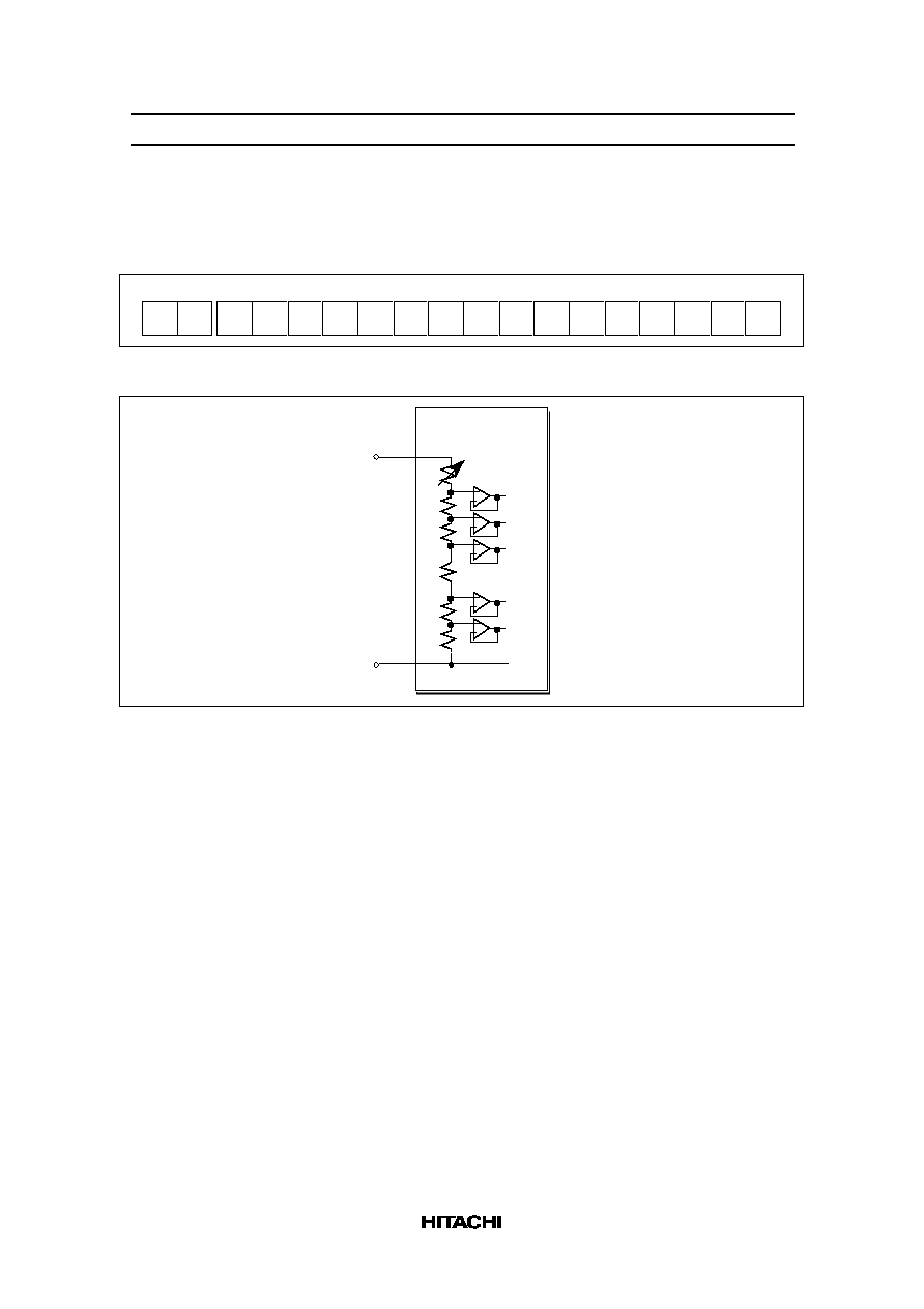
HD66750/1
28
Contrast Control
CT5–0: These bits control the LCD drive voltage (potential difference between V1 and GND) to adjust
64-step contrast. For details, see the Contrast Adjuster section.
0
1
*
CT1 CT0
R/W
RS
DB7
DB0
DB6 DB5
DB4 DB3
DB2
DB1
DB8
DB9
DB10
DB11
DB12
DB13
DB14
DB15
CT2
CT3
CT4
CT5
*
*
*
*
*
*
*
*
*
Figure 7 Contrast Control Instruction
V
LCD
V1
V2
V3
V4
V5
VR
R
R
R
0
R
R
-
+
-
+
-
+
-
+
-
+
GND
HD66750/1
GND
Figure 8 Contrast Adjuster

HD66750/1
29
Table 12
CT Bits and Variable Resistor Value of Contrast Adjuster
CT Set Value
CT5
CT4
CT3
CT2
CT1
CT0
Variable Resistor (VR)
0
0
0
0
0
0
3.20 x R
0
0
0
0
0
1
3.15 x R
0
0
0
0
1
0
3.10 x R
0
0
0
0
1
1
3.05 x R
0
0
0
1
0
0
3.00 x R
•
•
•
•
0
1
1
1
1
1
1.65 x R
1
0
0
0
0
0
1.60 x R
1
0
0
0
0
1
1.55 x R
1
0
0
0
1
0
1.50 x R
•
•
•
•
1
1
1
1
0
1
0.15 x R
1
1
1
1
1
0
0.10 x R
1
1
1
1
1
1
0.05 x R
Entry Mode
Rotation
The write data sent from the microcomputer is modified in the HD66750/1 and written to the CGRAM. The
display data in the CGRAM can be quickly rewritten to reduce the load of the microcomputer software
processing. For details, see the Graphics Operation Function section.
I/D: When I/D = 1, the address counter (AC) is automatically incremented by 1 after the data is written to
the CGRAM. When I/D = 0, the AC is automatically decremented by 1 after the data is written to the
CGRAM.
AM1–0: Set the automatic update method of the AC after the data is written to the CGRAM. When AM1–0
= 00, the data is continuously written in parallel. When AM1–0 = 01, the data is continuously written
vertically. When AM1–0 = 10, the data is continuously written vertically with two-word width (32-bit
length).
LG1–0: Write again the data read from the CGRAM and the data written from the microcomputer to the
CGRAM by a logical operation. When LG1–0 = 00, replace (no logical operation) is done. ORed when
LG1–0 = 01, ANDed when LG1–0 = 10, and EORed when LG1–0 = 11.
RT2–0: Write the data sent from the microcomputer to the CGRAM by rotating in a bit unit. RT3–0 specify
rotation. For example, when RT2–0 = 001, the data is rotated in the upper side by two bits. When RT2–0 =
111, the data is rotated in the upper side by 14 bits. The upper bit overflown in the most significant bit
(MSB) side is rotated in the least significant bit (LSB) side.
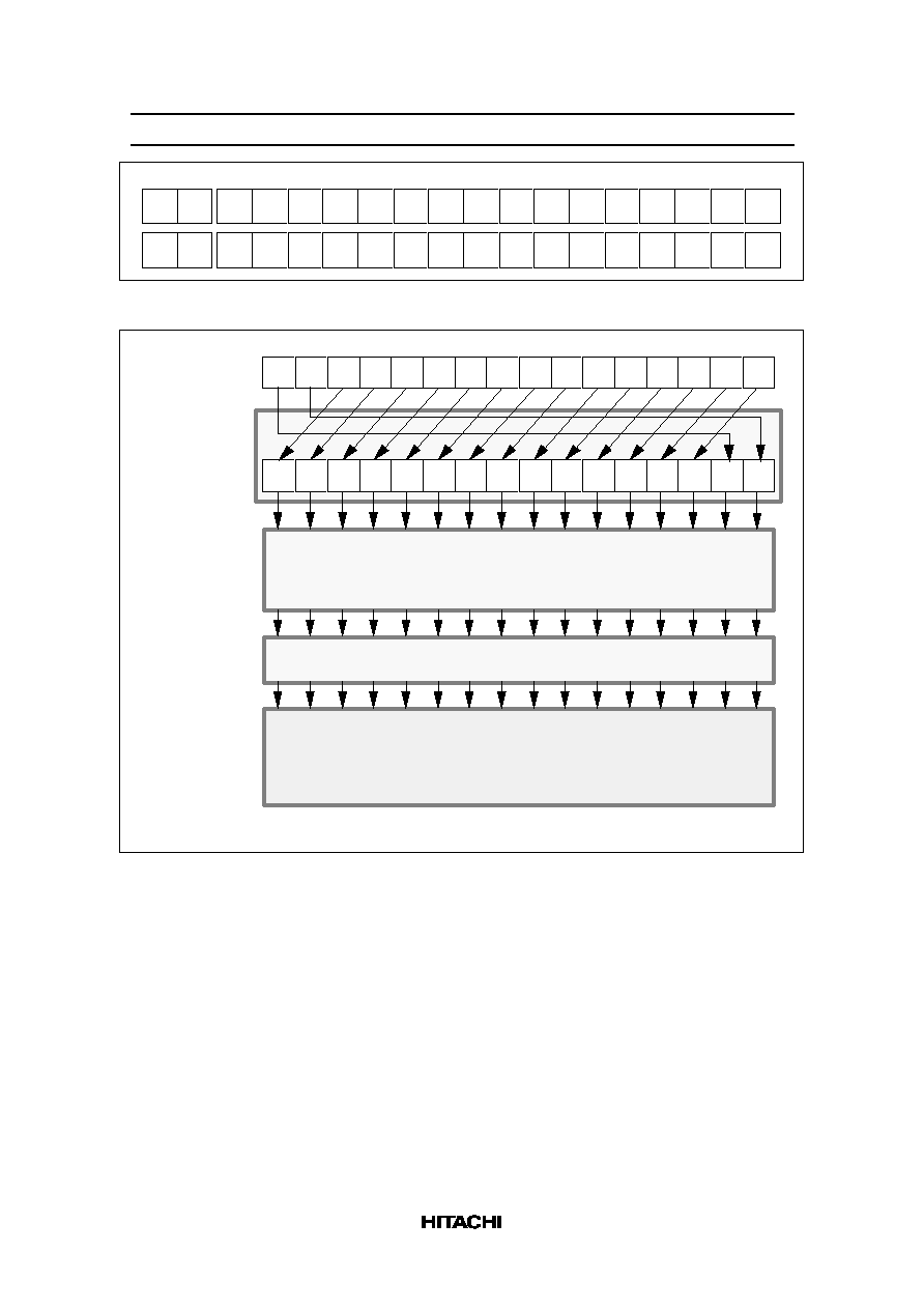
HD66750/1
30
0
1
R/W
RS
DB7
DB0
DB6 DB5
DB4 DB3
DB2
DB1
DB8
DB9
DB10
DB11
DB12
DB13
DB14
DB15
LG0
LG1
AM0
I/D AM1
*
*
0
1
RT1 RT0
RT2
*
*
*
*
*
*
*
*
*
*
*
*
*
*
*
*
*
*
*
*
*
*
Figure 9 Entry Mode and Rotation Instructions
0
0
0
1
1
DB7
DB0
DB6
DB5
DB4
DB3
DB2
DB1
DB8
DB9
DB10
DB11
DB12
DB13
DB14
DB15
1
0
0
1
1
1
0
0
0
1
1
0
0
0
1
1
1
0
0
1
1
1
0
0
0
1
1
Logical operation LG1–0 = 00: Replace
LG1–0 = 01: ORed
LG1–0 = 10: ANDed
LG1–0 = 11: EORed
Write data mask (WM15–0)
CGRAM
Write data sent
from the
microcomputer
(DB15–0)
Rotation
(RT2–0 = 001)
Logical operation
(LG1–0)
Write data mask*
(WM15–0)
Note: The write data mask (WM15–0) is set by the register in the RAM Write Data Mask section.
Figure 10 Logical Operation and Rotation for the CGRAM
HD66750/1
31
Display Control
PS1–0: When PS1–0 = 01, only the upper eight raster-rows (COM1–COM8) are fixed-displayed in vertical
smooth scrolling, and the other display raster-rows are smooth-scrolled. When PS1–0 = 10, the upper 16
raster-rows (COM1–COM16) are fixed-displayed. When PS1–0 = 11, the upper 24 raster-rows (COM1–
COM24) are fixed-displayed. For details, see the Partial Smooth Scroll Display Function section.
DHE: When DHE = 1, the double height between raster-rows specified in the Double-height Display
Position section is displayed. For details, see the Double-height Display section.
GS: When GS = 0, the grayscale level at a weak-colored display (DB = 01) is 1/3. When GS = 1, the
grayscale level at weak-colored display is 1/2, and at strong-colored display (when DB = 10) it is 2/3.
REV: Displays all character and graphics display sections with black-and-white reversal when REV = 1.
For details, see the Reversed Display Function section.
D: Display is on when D = 1 and off when D = 0. When off, the display data remains in the CGRAM, and
can be displayed instantly by setting D = 1. When D is 0, the display is off with the SEG1 to SEG128
outputs and COM1 to COM128 outputs set to the GND level. Because of this, the HD66750/1 can control
the charging current for the LCD with AC driving.
0
1
D
R/W
RS
DB7
DB0
DB6 DB5
DB4 DB3
DB2
DB1
DB8
DB9
DB10
DB11
DB12
DB13
DB14
DB15
*
*
*
*
*
*
*
REV
GS
DHE
PS1 PS0
*
*
*
Figure 11 Display Control Instruction
HD66750/1
32
Cursor Control
C: When C = 1, the window cursor display is started. The display mode is selected by the CM1–0 bits, and
the display area is specified in a dot unit by the horizontal cursor position register (HS6–0 and HE6–0 bits)
and vertical cursor position register (VS6–0 and VE6–0 bits). For details, see the Window Cursor Display
section.
CM1–0: The display mode of the window cursor is selected. These bits can display a white-blink cursor,
black-blink cursor, black-and-white reversed cursor, and black-and-white-reversed blink cursor.
0
1
CM0
R/W
RS
DB7
DB0
DB6 DB5
DB4 DB3
DB2
DB1
DB8
DB9
DB10
DB11
DB12
DB13
DB14
DB15
CM1
*
*
*
*
*
*
*
*
*
*
C
*
*
*
Figure 12 Cursor Control Instruction
Table 13
CM Bits and Window Cursor Display Mode
CM1
CM0
Window Cursor Display Mode
0
0
White-blink cursor (alternately blinking between the normal display and an all-white
display (all unlit))
0
1
Black-blink cursor (alternately blinking between the normal display and an all-black
display (all lit))
1
0
Black-and-white reversed cursor (black-and-white-reversed normal display (no
blinking))
1
1
Black-and-white-reversed blink cursor (alternately blinking the black-and-white-
reversed normal display)
Double-height Display Position
DS6–0: Specify any common raster-row position where the double-height display starts. Note that no
scrolling is done by vertical scrolling. For details, see the Double-height Display section.
DE6-0: Specify any common raster-row position where the double-height display ends. Set the end
position of the double-height display after the start position of the double-height display, satisfying the
relationship DS6–0
DE6–0. When the area specifying the double height has an odd number of raster-
rows, the double-height display is done for the DE6–0 + 1 raster-rows.
When the double-height display is not used, set the DHE bit in the display-control instruction register to 0.
0
1
R/W
RS
DB7
DB0
DB6 DB5
DB4 DB3
DB2
DB1
DB8
DB9
DB10
DB11
DB12
DB13
DB14
DB15
*
DS6 DS5 DS4 DS3 DS2 DS1 DS0
*
DE6 DE5 DE4 DE3 DE2 DE1 DE0
Figure 13 Double-height Display Position Instruction
HD66750/1
33
Vertical Scroll Control
SL6–0: Specify the display start raster-row for vertical smooth scrolling. Any raster-row from the first to
128th can be selected (table 14). After the 128th raster-row is displayed, the display restarts from the first
raster-row. For details, see the Vertical Smooth Scroll section.
In partial smooth scrolling, these bits specify the display start raster-row of the next fixed-display raster-
row. For details, see the Partial Smooth Scroll Display Function section.
0
1
SL1 SL0
R/W
RS
DB7
DB0
DB6 DB5
DB4 DB3
DB2
DB1
DB8
DB9
DB10
DB11
DB12
DB13
DB14
DB15
SL2
*
SL6 SL5 SL4 SL3
*
*
*
*
*
*
*
*
Figure 14 Vertical Scroll Control Instruction
Table 14
SL Bits and Display-start Raster-row
SL6
SL5
SL4
SL3
SL2
SL1
SL0
Display-start Raster-row
0
0
0
0
0
0
0
1st raster-row
0
0
0
0
0
0
1
2nd raster-row
0
0
0
0
0
1
0
3rd raster-row
0
0
0
0
0
1
1
4th raster-row
0
0
0
0
1
0
0
5th raster-row
:
:
:
:
:
:
:
:
1
1
1
1
1
1
0
127th raster-row
1
1
1
1
1
1
1
128th raster-row
HD66750/1
34
Horizontal Cursor Position
Vertical Cursor Position
HS6-0: Specify the start position for horizontally displaying the window cursor in a dot unit. The cursor is
displayed from the 'set value + 1' dot. Ensure that HS6–0
HE6–0.
HE6-0: Specify the end position for horizontally displaying the window cursor in a dot unit. The cursor is
displayed to the 'set value + 1' dot. Ensure that HS6–0
HE6–0.
VS6-0: Specify the start position for vertically displaying the window cursor in a dot unit. The cursor is
displayed from the 'set value + 1' dot. Ensure that VS6–0
VE6–0.
VE6-0: Specify the end position for vertically displaying the window cursor in a dot unit. The cursor is
displayed to the 'set value + 1' dot. Ensure that VS6–0
VE6–0. In vertical scrolling, rewrite VS6–0 and
VE6–0 since this window cursor does not move vertically.
0
1
HS1 HS0
R/W
RS
DB7
DB0
DB6 DB5
DB4 DB3
DB2
DB1
DB8
DB9
DB10
DB11
DB12
DB13
DB14
DB15
HS2
*
HS6 HS5 HS4 HS3
0
1
VS1 VS0
VS2
*
VS6 VS5 VS4 VS3
HE1 HE0
HE2
*
HE6 HE5 HE4 HE3
VE1 VE0
VE2
*
VE6 VE5 VE4 VE3
Figure 15 Horizontal Cursor Position and Vertical Cursor Position Instructions
Window
cursor
HS1+1
HE1+1
VS1+1
VE1+1
Figure 16 Window Cursor Position
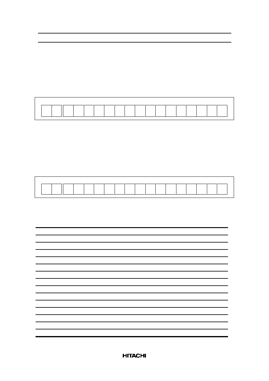
HD66750/1
35
RAM Write Data Mask
WM15-0: In writing to the CGRAM, these bits mask writing in a bit unit. When WM15 = 1, this bit masks
the write data of DB15 and does not write to the CGRAM. Similarly, the WM14–0 bits mask the write data
of DB14–0 in a bit unit. However, when AM = 10, the write data is masked with the set values of VM15–0
for the odd-times CGRAM write. It is also masked automatically with the reversed set values of VM15–0
for the even-times CGRAM write. For details, see the Graphics Operation Function section.
0
1
R/W
RS
DB7
DB0
DB6 DB5
DB4 DB3
DB2
DB1
DB8
DB9
DB10
DB11
DB12
DB13
DB14
DB15
VM
7
VM
6
VM
5
VM
4
VM
3
VM
2
VM
1
VM
0
VM
15
VM
14
VM
13
VM
12
VM
11
VM
10
VM
9
VM
8
Figure 17 RAM Write Data Mask Instruction
RAM Address Set
AD10-0: Initially set CGRAM addresses to the address counter (AC). Once the CGRAM data is written,
the AC is automatically updated according to the AM1–0 and I/D bit settings. This allows consecutive
accesses without resetting addresses. Once the CGRAM data is read, the AC is not automatically updated.
CGRAM address setting is not allowed in the sleep mode or standby mode.
0
1
R/W
RS
DB7
DB0
DB6 DB5
DB4 DB3
DB2
DB1
DB8
DB9
DB10
DB11
DB12
DB13
DB14
DB15
AD
10
AD9 AD8 AD7 AD6 AD5 AD4 AD3 AD2 AD1 AD0
*
*
*
*
*
Figure 18 RAM Address Set Instruction
Table 15
AD Bits and CGRAM Settings
AD10–AD0
CGRAM Setting
"000"H–"00F"H
Bitmap data for COM1
"010"H–"01F"H
Bitmap data for COM2
"020"H–"02F"H
Bitmap data for COM3
"030"H–"03F"H
Bitmap data for COM4
:
:
"760"H–"76F"H
Bitmap data for COM119
"770"H–"77F"H
Bitmap data for COM120
"780"H–"78F"H
121st raster-row data (appeared at vertical scrolling)
"790"H–"79F"H
122nd raster-row data (appeared at vertical scrolling)
"7A0"H–"7AF"H
123rd raster-row data (appeared at vertical scrolling)
"7B0"H–"7BF"H
124th raster-row data (appeared at vertical scrolling)
"7C0"H–"7CF"H
125th raster-row data (appeared at vertical scrolling)
"7D0"H–"7DF"H
126th raster-row data (appeared at vertical scrolling)
"7E0"H–"7EF"H
127th raster-row data (appeared at vertical scrolling)
"7F0"H–"7FF"H
128th raster-row data (appeared at vertical scrolling)

HD66750/1
36
Write Data to CGRAM
WD15-0 : Write 16-bit data to the CGRAM. After a write, the address is automatically updated according
to the AM1–0 and I/D bit settings. During the sleep and standby modes, the CGRAM cannot be accessed.
0
1
R/W
RS
DB7
DB0
DB6 DB5
DB4 DB3
DB2
DB1
DB8
DB9
DB10
DB11
DB12
DB13
DB14
DB15
WD
15
WD
14
WD
13
WD
12
WD
11
WD
10
WD
9
WD
8
WD
7
WD
6
WD
5
WD
4
WD
3
WD
2
WD
1
WD
0
Figure 19 Write Data to CGRAM Instruction
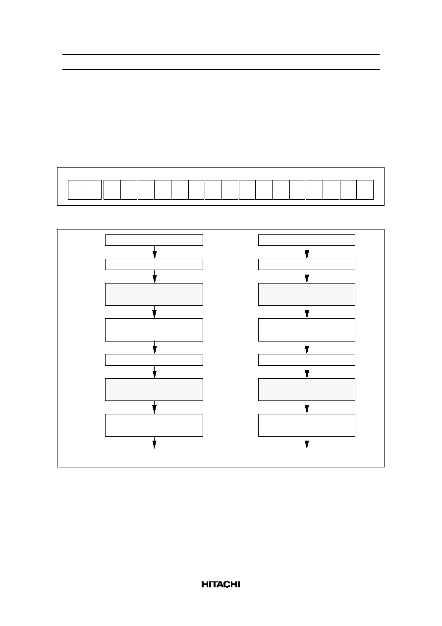
HD66750/1
37
Read Data from CGRAM
RD15-0 : Read 16-bit data from the CGRAM. When the data is read to the microcomputer, the first-word
read immediately after the CGRAM address setting is latched from the CGRAM to the internal read-data
latch. The data on the data bus (DB15–0) becomes invalid and the second-word read is normal.
When bit processing, such as a logical operation, is performed within the HD66750/1, only one read can be
processed since the latched data in the first word is used.
1
1
R/W
RS
DB7
DB0
DB6 DB5
DB4 DB3
DB2
DB1
DB8
DB9
DB10
DB11
DB12
DB13
DB14
DB15
RD
15
RD
14
RD
13
RD
12
RD
11
RD
10
RD
9
RD
8
RD
7
RD
6
RD
5
RD
4
RD
3
RD
2
RD
1
RD
0
Figure 20 Read Data from CGRAM Instruction
Address: N set
Dummy read (invalid data)
CGRAM -> Read-data latch
Read (data of address n)
Read-data latch -> DB15–0
First word
Second word
i) Data read to the microcomputer
ii) Logical operation processing in the HD66750/1
Address: M set
Dummy read (invalid data)
CGRAM -> Read-data latch
Read (data of address)
Read-data latch -> DB15–0
First word
Second word
Sets the I/D and AM1–0 bits
Address: N set
Dummy read (invalid data)
CGRAM -> Read-data latch
Sets the I/D and AM1–0 bits
Read (data of address n)
DB15–0 -> CGRAM
Dummy read (invalid data)
CGRAM -> Read-data latch
Write (data of address n)
DB15–0 -> CGRAM
Automatic address update: M +
First word
Second word
First word
Second word
Figure 21 CGRAM Read Sequence
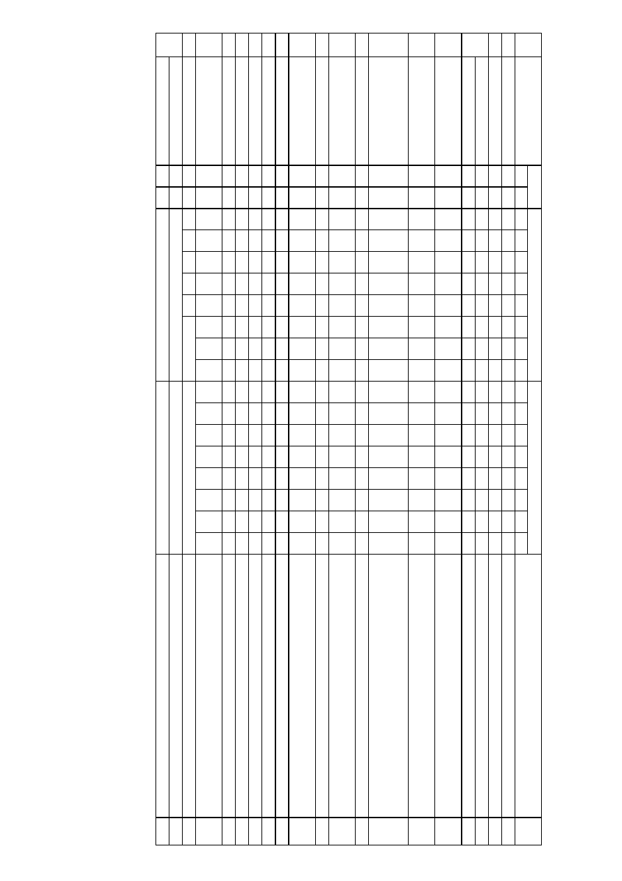
Table 16 Instruction List
Reg.
Upper Code
Lower Code
No.
Register Name
R/W
RS DB15 DB14 DB13 DB12 DB11 DB10 DB9 DB8 DB7 DB6 DB5 DB4 DB3 DB2 DB1 DB0
Description
IR
Index
0
0
*
*
*
*
*
*
*
*
*
*
*
ID4
ID3
ID2
ID1
ID0
Sets the index register value.
0
SR
Status read
1
0
0
L6
L5
L4
L3
L2
L1
L0
0
0
C5
C4
C3
C2
C1
C0
Reads the driving raster-row position (L6–0) and contrast setting (C5–0).
0
R00
Start oscillation
0
1
*
*
*
*
*
*
*
*
*
*
*
*
*
*
*
1
Starts the oscillation mode.
10 ms
Device code read
1
1
0
0
0
0
0
1
1
1
0
1
0
1
0
0
0
0
Reads 0750H.
0
R01
Driver output
0
1
*
*
*
*
*
*
CMS SGS
*
CN
*
*
NL3
NL2
NL1
NL0
Sets the common driver shift direction (CMS), segment driver shift direction
0
control
(SGS), driving duty ratio (NL3–0), and centering (CN).
R02
LCD-driving-
0
1
*
*
*
*
*
*
*
*
*
B/C
EOR NW4 NW3 NW2 NW1 NW0 Sets the LCD drive AC waveform (B/C), and EOR output (EOR) or the
0
waveform control
number of n-raster-rows (NW4–0) at C-pattern AC drive.
R03
Power control
0
1
*
*
*
BS2
BS1
BS0
BT1
BT0
*
*
DC1 DC0
AP1
AP0
SLP
STB
Sets the sleep mode (SLP), standby mode (STB), LCD power on (AP1–0),
0
boosting cycle (DC1–0), boosting ouput multiplying factor (BT1–0), and LCD
drive bias value (BS2–0).
R04
Contrast control
0
1
*
*
*
*
*
*
*
*
*
*
CT5
CT4
CT3
CT2
CT1
CT0
Sets the contrast adjustment (CT5–0).
0
R05
Entry mode
0
1
*
*
*
*
*
*
*
*
*
*
*
I/D
AM1 AM0 LG1
LG0
Specifies the logical operation (LG1–0), AC counter mode (AM1–0), and
0
increment/decrement mode (I/D).
R06
Rotation
0
1
*
*
*
*
*
*
*
*
*
*
*
*
*
RT2
RT1
RT0
Specifies the amount of write-data rotation (RT2–0).
0
R07
Display control
0
1
*
*
*
*
*
*
*
*
*
*
PS1
PS0 DHE
GS
REV
D
Specifies display on (D), black-and-white reversed display (REV), grayscale
0
mode (GS), double-height display on (DHE), and partial scroll (PS1–0).
R08
Cursor control
0
1
*
*
*
*
*
*
*
*
*
*
*
*
*
C
CM1 CM0 Specifies cursor display on (C) and cursor display mode (CM1–0).
R09
Double-height display position
0
1
*
DE6 DE5 DE4 DE3 DE2 DE1 DE0
*
DS6 DS5 DS4 DS3 DS2 DS1 DS0
Specifies double-height display start (DS6–0) and end (DE6–0).
0
R0A
Vertical scroll
0
1
*
*
*
*
*
*
*
*
*
SL6
SL5
SL4
SL3
SL2
SL1
SL0
Sets the display-start raster-row (SL6–0).
0
R0B
Horizontal cursor position
0
1
*
HE6 HE5 HE4 HE3 HE2 HE1 HE0
*
HS6 HS5 HS4 HS3 HS2 HS1 HS0
Sets horizontal cursor start (HS6–0) and end (HE6–0).
0
R0C
Vertical cursor position
0
1
*
VE6
VE5
VE4
VE3
VE2
VE1
VE0
*
VS6
VS5
VS4
VS3
VS2
VS1
VS0
Sets vertical cursor start (VS6–0) and end (VE6–0).
0
R10
RAM write data
0
1
WM
WM
WM
WM
WM
WM WM9 WM8 WM7 WM6 WM5 WM4 WM3 WM2 WM1 WM0 Specifies write data mask (WM15–0) at RAM write.
0
mask
15
14
13
12
11
10
R11
RAM address set
0
1
*
*
*
*
*
AD10–8 (upper)
AD7–0 (lower)
Initially sets the RAM address to the address counter (AC).
0
R12
RAM data write
0
1
Write data (upper)
Write data (lower)
Writes data to the RAM.
0
RAM data read
1
1
Read data (upper)
Read data (lower)
Reads data from the RAM.
0
Note: '*' means 'doesn't matter'.
Execu-
tion
Cycle
HITACHI
38

HD66750/1
39
Reset Function
The HD66750/1 is internally initialized by RESET input. Because the busy flag (BF) indicates a busy state
(BF = 1) during the reset period, no instruction or CGRAM data access from the MPU is accepted. The
reset input must be held for at least 1 ms. Do not access the CGRAM or initially set the instructions until the
R-C oscillation frequency is stable after power has been supplied (10 ms).
Instruction Set Initialization:
1. Start oscillation executed
2. Driver output control (CN = 0, NL3–0 = 1111, SGS = 0, CMS = 0)
3. B-pattern waveform AC drive (B/C = 0, ECR = 0, NW4–0 = 00000)
4. Power control (DC1–0 = 00, AP1–0 = 00: LCD power off, SLP = 0: Sleep mode off, STB = 0: Standby
mode off)
5. 1/11 bias drive (BS2–0 = 000), Two-times boost (BT1–0 = 00), Weak contrast (CT5–0 = 000000)
6. Entry mode set (I/D = 1: Increment by 1, AM1–0 = 00: Horizontal move, LG1–0 = 00: Replace mode)
7. Rotation (RT2–0 = 000: No shift)
8. Display control (DHE = 0: Double-height display off, REV = 0, GS = 0, D = 0: Display off, PS1–0 =
00: Partial scroll off)
9. Cursor control (C = 0: Cursor display off, CM1–0 = 00: White blink cursor)
10. Double-height display position (DS6–0 = 0000000, DE6–0 = 0000000)
11. Vertical scroll control (SL6–0 = 0000000: First raster-row displayed at the top)
12. Window cursor display position (HS6–0 = HE6–0 = VS6–0 = VE6–0 = 0000000)
13. RAM write data mask (WM15–0 = 0000H: No mask)
14. RAM address set (AD10–0 = 000H)
CGRAM Data Initialization:
This is not automatically initialized by reset input but must be initialized by software while display is off
(D = 0).
Output Pin Initialization:
1. LCD driver output pins (SEG/COM): Outputs GND level
2. Booster output pins (VLOUT): Outputs Vcc level
3. Oscillator output pin (OSC2): Outputs oscillation signal

HD66750/1
40
Parallel Data Transfer
16-bit Bus Interface
Setting the IM2≠0 (interface mode) to the GND/GND level allows 68-system E-clock-synchronized 16-bit
parallel data transfer. Setting the IM1/0 to the Vcc/GND level allows 80-system 16-bit parallel data
transfer. When the number of buses or the mounting area is limited, use an 8-bit bus interface.
CSn*
A1
HWR*
(RD*)
D15≠D0
CS*
RS
WR*
(RD*)
DB15≠DB0
H8/2245
HD66750/1
16
Figure 22 Interface to 16-bit Microcomputer
8-bit Bus Interface
Setting the IM1/0 (interface mode) to the GND/Vcc level allows 68-system E-clock-synchronized 8-bit
parallel data transfer using pins DB15≠DB8. Setting the IM1/0 to the Vcc/Vcc level allows 80-system 8-
bit parallel data transfer. The 16-bit index register, instructions and RAM data are divided into eight
upper/lower bits and the transfer starts from the upper eight bits. Fix unused pins DB7≠DB0 to the Vcc or
GND level.
CSn*
A1
HWR*
(RD*)
D15≠D8
CS*
RS
WR*
(RD*)
DB15≠DB8
DB7≠0
H8/2245
HD66750/1
8
8
GND
Figure 23 Interface to 8-bit Microcomputer
Note:
Transfer synchronization function for an 8-bit bus interface
The HD66750/1 supports the transfer synchronization function which resets the upper/lower
counter to count upper/lower 8-bit data transfer in the 8-bit bus interface. Noise causing transfer
mismatch between the eight upper and lower bits can be corrected by a reset triggered by
consecutively writing a 00H instruction four times. The next transfer starts from the upper eight
bits. Executing synchronization function periodically can recover any runaway in the display
system.
HD66750/1
41
00H
00H
00H
00H
RS
R/W
E
DB15–
DB8
Upper
Lower
(8-bit transfer synchronization)
(1)
(2)
(3)
(4)
Upper/
lower
Figure 24 8-bit Transfer Synchronization

HD66750/1
42
Graphics Operation Function
The HD66750/1 can greatly reduce the load of the microcomputer graphics software processing through the
16-bit bus architecture and graphics-bit operation function. This function supports the following:
1. A write data mask function that selectively rewrites some of the bits in the 16-bit write data.
2. A bit rotation function that shifts and writes the data sent from the microcomputer in a bit unit.
3. A logical operation function that writes the data sent from the microcomputer and the original RAM
data by a logical operation.
S inc e t he di s pla y dat a i n t he gra phi cs R AM (C GR AM ) ca n be qui ckl y re wri t t en, t he l oad of t he
m i croc om pute r proc es s i ng ca n be re duce d i n t he l ar ge di s pla y s cr ee n whe n a font pat t er n, s uch as kanj i
characters, is developed for any position (BiTBLT processing).
The gra phi cs bi t oper at i on ca n be cont r oll e d by com bi ni ng t he ent r y m ode re gi st e r, t he bi t s et val ue of t he
RAM-write-data mask register, and the read/write from the microcomputer.
Table 17
Graphics Operation
Bit Setting
Operation Mode
I/D
AM
LG
Operation and Usage
Write mode 1
0/1
00
00
Horizontal data replacement, horizontal-border
drawing
Write mode 2
0/1
01
00
Vertical data replacement, font development, vertical-
border drawing
Write mode 3
0/1
10
00
Vertical data replacement with two-word width, kanji-
font development
Read/write mode 1
0/1
00
01 10 11
Horizontal data replacement with logical operation,
horizontal-border drawing
Read/write mode 2
0/1
01
01 10 11
Vertical data replacement with logical operation,
vertical-border drawing
Read/write mode 3
0/1
10
01 10 11
Horizontal data replacement with two-word-width
logical operation

HD66750/1
43
Read-
data
latch
Bit rotation
Logical operation
Write bit mask
Write-data latch
Graphics RAM
(CGRAM)
Microcomputer
Address
counter
(AC)
Rotation bit
(RT2–0)
Logical
operation
bit
(LG1–0)
2
3
16
16
Write-mask register
(WM15–0)
16
11
16
+1/–1
+16
16
16
16
HD66750/1
00: through
01: OR
10: AND
11: EOR
Figure 25 Data Processing Flow of the Graphics Bit Operation
1. Write mode 1: AM1–0 = 00, LG1–0 = 00
This mode is used when the data is horizontally written at high speed. It can also be used to initialize the
gra phi cs R AM (C GR AM ) or t o dra w borde rs . The rot a ti on func t ion (R T2–0) or wr it e -dat a m as k
func t ion (W M 15–0) ar e al s o ena bl ed i n t hes e oper at i ons . Af te r wr it i ng, t he addr es s count e r (A C)
aut om at i ca l ly i ncr em ent s by 1 (I /D = 1) or dec re me nt s by 1 (I /D = 0), and aut om at i ca l ly j um ps t o t he
counter edge one-raster-row below after it has reached the left edge of the graphics RAM.
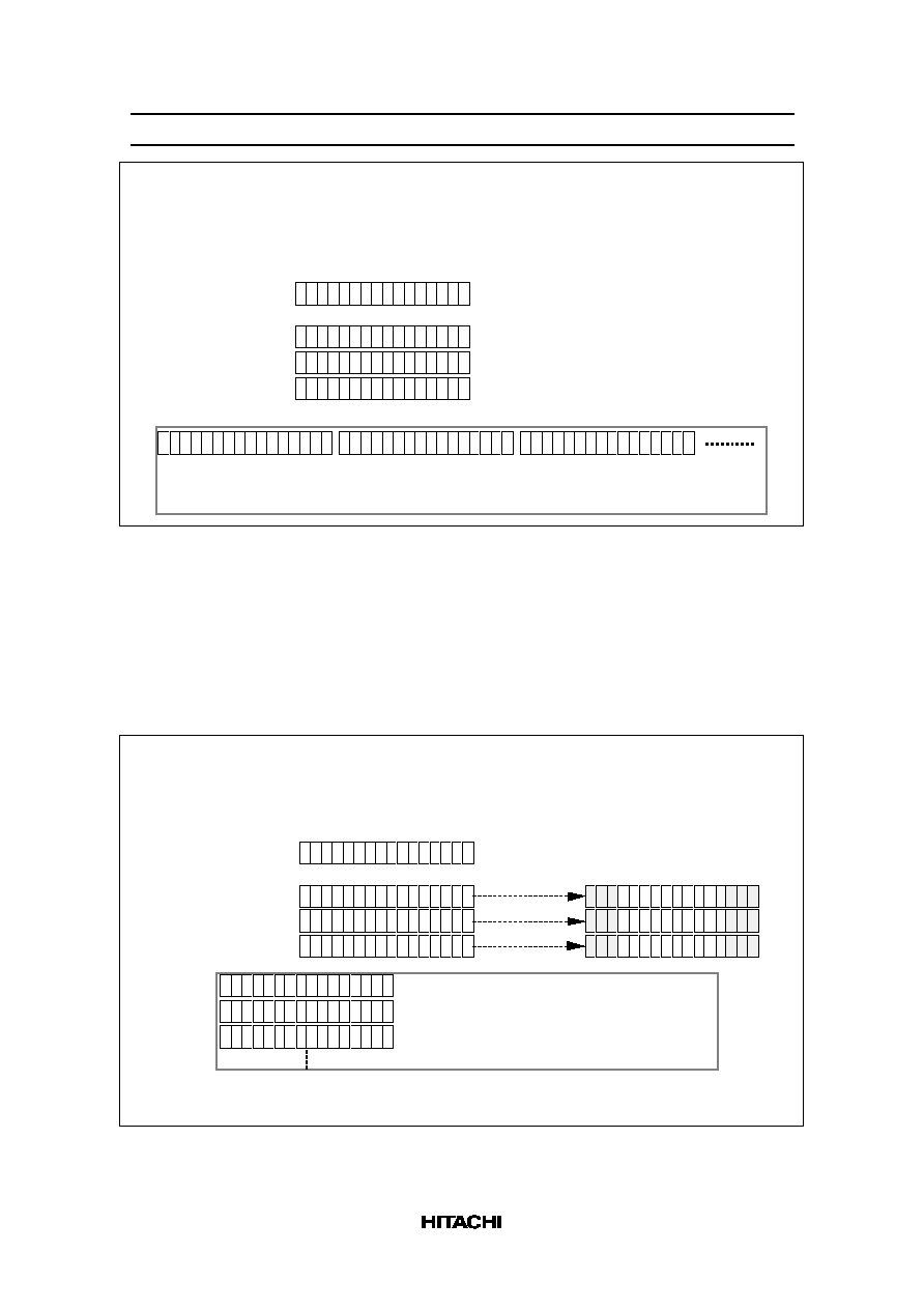
HD66750/1
44
WM0
WM15
0 0 0 0 0 0 0 0 0 0 0 0 0 0 0 0
DB0
DB15
1 0 0 1 1 0 0 1 0 1 0 0 0 0 1 1
1 1 0 0 0 0 1 1 0 0 0 0 1 1 0 0
0 1 1 1 0 1 0 0 0 0 0 1 1 1 1 1
1 0 0 1 1 0 0 1 0 1 0 0 0 0 1 1
1 1 0 0 0 0 1 1 0 0 0 0 1 1 0 0
0 1 1 1 0 1 0 0 0 0 0 1 1 1 1 1
000H
001H
002H
CGRAM
1) I/D = 1, AM1–0 = 00, LG1–0 = 00, RT2–0 = 000
2) WM15–0 = 0000H
3) AC = 000H
Operation Examples:
Write data mask:
Write data (1) :
Write data (2) :
Write data (3) :
Write data (1)
Write data (2)
Write data (3)
Figure 26 Writing Operation of Write Mode 1
2. Write mode 2: AM1–0 = 01, LG1–0 = 00
Thi s m ode i s us ed whe n t he dat a i s ver t ic al l y wr it t en at hi gh s pee d. It ca n al s o be us ed t o i ni ti a li z e t he
gra phi cs R AM (C GR AM ), deve l op t he font pat t er n i n t he ver t ic al di re ct i on, or dra w borde rs . The
rotation function (RT2–0) or write-data mask function (WM15–0) are also enabled in these operations.
After writing, the address counter (AC) automatically increments by 16, and automatically jumps to the
upper-right edge (I/D = 1) or upper-left edge (I/D = 0) following the I/D bit after it has reached the lower
edge of the graphics RAM.
WM0
WM15
1) I/D = 1, AM1–0 = 01, LG1–0 = 00, RT2–0 = 010
2) WM15–0 = F007H
3) AC = 000H
Write data mask:
1 1 1 0 0 0 0 0 0 0 0 0 1 1 1 1
DB0
DB15
Write data (1) :
1 0 0 1 1 0 0 1 0 1 0 0 0 0 1 1
Write data (2) :
1 1 0 0 0 0 1 1 0 0 0 0 1 1 0 0
Write data (3) :
0 1 1 1 0 1 0 0 0 0 0 1 1 1 1 1
000H
CGRAM
0 1 0 0
0 0 1
0 0 0 0
1 1 0
0 0 0 1
1 1 1
1 0 0 1 1 0 0 1
1
1 1 0 0 0 0 1 1
0
0 1 1 1 0 1 0 0
1
4-bit rotation
010H
020H
*
*
*
*
*
*
*
*
*
*
*
*
*
*
*
*
*
*
*
*
*
1 0 0 1 1 0 0 1
1
1 1 0 0 0 0 1 1
0
0 1 1 1 0 1 0 0
1
4-bit rotation
4-bit rotation
Operation Examples:
Write data (1)
Write data (2)
Write data (3)
Notes: 1. The bit area data in the RAM indicated by '*' is not changed.
2. After writing to address 7F0H, the AC jumps to 001H.
Figure 27 Writing Operation of Write Mode 2
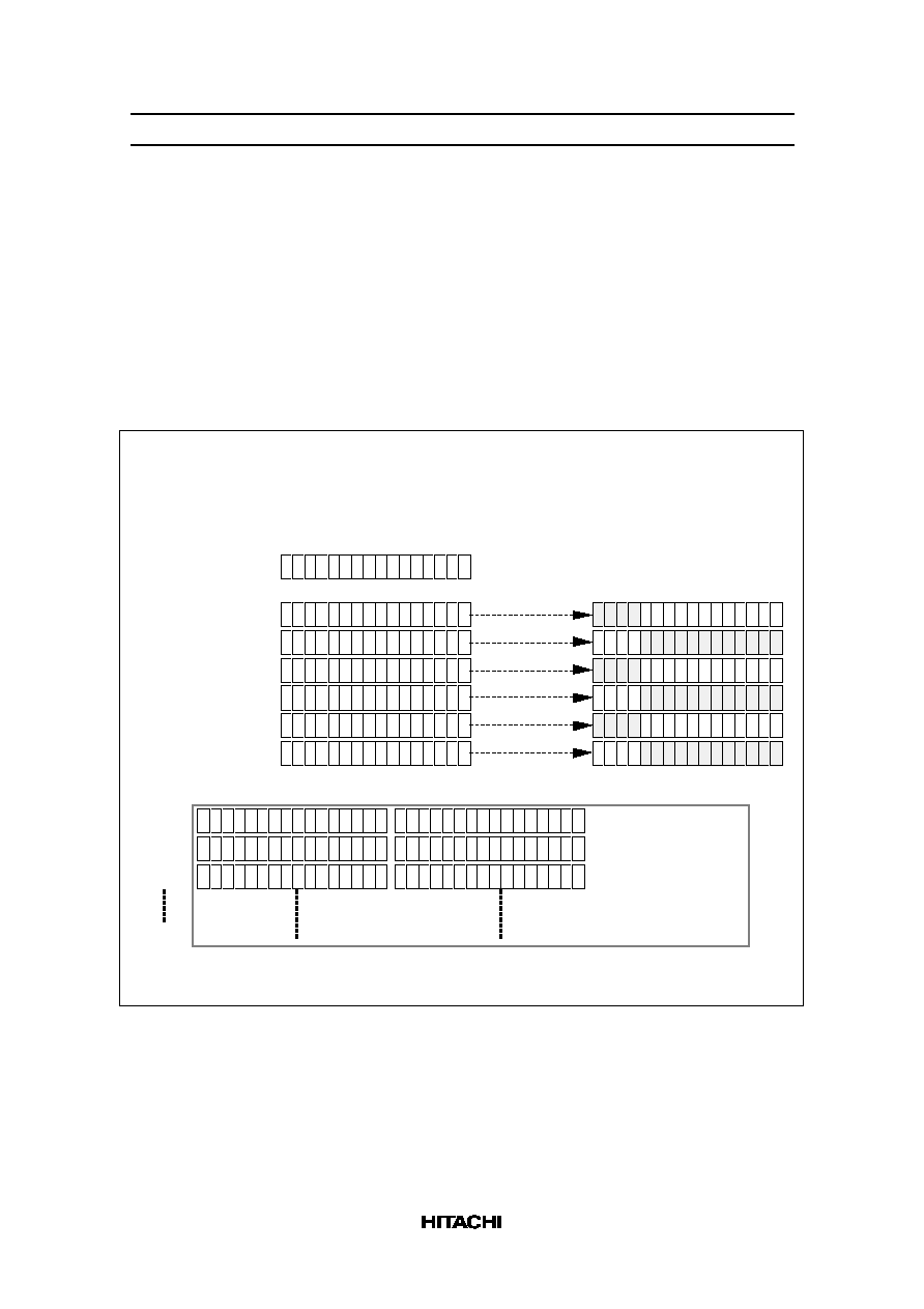
HD66750/1
45
3. Write mode 3: AM1–0 = 10, LG1–0 = 00
This mode is used when the data is written at high speed by vertically shifting bits. It can also be used to
wr it e t he 16-bi t dat a for t wo wor ds i nt o t he gra phi cs R AM (C GR AM ), deve l op t he font pat t er n, or
transfer the BiTBLT as a bit unit. The rotation function (RT2–0) or write-data mask function (WM15–0)
ar e al s o ena bl ed i n t hes e oper at i on. Howe ver , al t hough t he wr it e -dat a m as k func t ion m as ks t he bi t
pos i ti on s et wi t h t he wr it e -dat a m as k re gi st e r (W M 15–0) at t he odd-t i m es (s uc h as t he fi rs t or t hi rd)
wr it e , t he func t ion m as ks t he bi t pos i ti on t hat re ver se d t he s et t i ng val ue of t he wr it e -dat a m as k re gi st e r
(W M 15–0) at t he eve n-t i m es (s uc h as t he s ec ond or four th) wr it e . Af ter t he odd-t i m es wr it i ng, t he
addr es s count e r (A C) aut om at i ca l ly i ncr em ent s by 1 (I /D = 1) or dec re me nt s by 1 (I /D = 0). Af te r t he
even-times writing, the AC automatically increments or decrements by –1 + 16 (I/D = 1) or +1 + 16 (I/D
= 0). The AC automatically jumps to the upper edge after it has reached the lower edge of the graphics
RAM.
WM0
WM15
1 1 1 1 0 0 0 0 0 0 0 0 0 0 0 0
DB0
DB15
1 1 1 1 1 1 0 0 0 0 0 1 1 0 0 0
1 1 1 1 1 1 0 0 0 0 0 1 1 0 0 0
0 0 0 0 0 1 1 1 0 0 0 0 1 1 1 1
000H
Write data (1), (2)
CGRAM
010H
020H
Write data (3), (4)
Write data (5), (6)
*
0 0 0 0 0 1 1 1 0 0 0 0 1 1 1 1
1 1 1 1 1 1 0 0 0 0 0 1
1 0 0 0
1 1 1 1 1 1 0 0 0 0 0 1
1 0 0 0
0 0 0 0 0 1 1 1 0 0 0 0
1 1 1 1
0 0 0 0 0 1 1 1 0 0 0 0
1 1 1 1
1 1 1 1 1 1 0 0 0 0 0 1
0 0 0 0 0 1 1 1 0 0 0 0
1 0 0 0
1 1 1 1
*
*
*
*
*
*
*
*
*
*
*
*
*
*
*
*
*
*
*
*
*
*
*
*
*
*
*
*
*
*
*
000H
001H
0 0 1 0 0 0 0 1 1 1 1 1 1 0 0 0
0 0 1 0 0 0 0 1 1 1 1 1 1 0 0 0
0 0 1 0 0 0 0 1 1 1 1 1
1 0 0 0
0 0 1 0 0 0 0 1 1 1 1 1
1 0 0 0
*
*
*
*
* * * * * * * * * * * *
0 0 1 0 0 0 0 1 1 1 1 1
1 0 0 0
7F0H
1) I/D = 1, AM1–0 = 10, LG1–0 = 00, RT2–0 = 010
2) WM15–0 = 0007H
3) AC = 000H
Write data mask:
Write data (1) :
Write data (2) :
Write data (3) :
4-bit rotation
4-bit rotation
4-bit rotation
Operation Examples:
Write data (4) :
Write data (5) :
Write data (6) :
4-bit rotation
4-bit rotation
4-bit rotation
Notes: 1. The bit area data in the RAM indicated by '*' is not changed.
2. After writing to address 7F0H, the AC jumps to 001H.
Figure 28 Writing Operation of Write Mode 3

HD66750/1
46
4. Read/Write mode 1: AM1–0 = 00, LG1–0 = 01/10/11
This mode is used when the data is horizontally written at high speed by performing a logical operation
wi t h t he ori gi nal dat a . It re ads t he di s pla y dat a (or igi na l dat a ), whi ch has al r eady bee n wr it t en i n t he
gra phi cs R AM (C GR AM ), per form s a l ogi cal oper at i on wi t h t he wr it e dat a s ent fr om t he
microcomputer, and rewrites the data to the CGRAM. This mode can read the data during the same bus
cycle as for the write operation since the read operation of the original data does not latch the read data
into the microcomputer and temporarily holds it in the read-data latch. The rotation function (RT2–0) or
wr it e -dat a m as k func t ion (W M 15–0) ar e al s o ena bl ed i n t hes e oper at i ons . Af te r wr it i ng, t he addr es s
count e r (A C) aut om at i ca l ly i ncr em ent s by 1 (I /D = 1) or dec re ment s by 1 (I /D = 0), and aut om at i ca l ly
jumps to the counter edge one-raster-row below after it has reached the left or right edges of the graphics
RAM.
WM0
WM15
Write data mask:
0 0 0 0 0 0 0 0 0 0 0 0 0 0 0 0
DB0
DB15
Write data (1):
1 0 1 1 1 1 0 0 0 1 1 0 0 0 0 1
Write data (2):
1 1 0 0 0 0 1 1 1 0 0 0 1 1 0 0
Write data (3):
0 1 1 1 0 1 0 0 0 0 0 1 1 1 1 1
000H
001H
002H
Read data (1) + Write data (1)
CGRAM
Read data (1):
1 0 0 1 1 0 0 1 0 1 0 0 0 0 1 1
Read data (2):
0 0 0 0 1 1 1 1 0 0 0 0 0 0 0 0
Read data (3):
0 0 0 0 1 1 1 0 1 0 0 0 0 1 1 0
1 0 1 1 1 1 0 1 0 1 1 0 0 0 1 1
1 1 0 0 1 1 1 1 1 0 0 0 1 1 0 0
0 1 1 1 1 1 1 0 1 0 0 1 1 1 1 1
Logical operation
(OR)
Logical operation
(OR)
Logical operation
(OR)
0 1 1 1 1 1 1 0 1 0 0 1 1 1 1 1
1 1 0 0 1 1 1 1 1 0 0 0 1 1 0 0
1 0 1 1 1 1 0 1 0 1 1 0 0 0 1 1
Read data (2) + Write data (2) Read data (3) + Write data (3)
1) I/D = 1, AM1–0 = 00, LG1–0 = 01 (OR), RT2–0 = 000
2) WM15–0 = 0000H
3) AC = 000H
Operation Examples:
Figure 29 Writing Operation of Read/Write Mode 1
5. Read/Write mode 2: AM1–0 = 01, LG1–0 = 01/10/11
Thi s m ode i s us ed whe n t he dat a i s ver t ic al l y wr it t en at hi gh s pee d by per form i ng a l ogi cal oper at i on
wi t h t he ori gi nal dat a . It re ads t he di s pla y dat a (or igi na l dat a ), whi ch has al r eady bee n wr it t en i n t he
gra phi cs R AM (C GR AM ), per form s a l ogi cal oper at i on wi t h t he wr it e dat a s ent fr om t he
microcomputer, and rewrites the data to the CGRAM. This mode can read the data during the same bus
cycle as for the write operation since the read operation of the original data does not latch the read data
into the microcomputer and temporarily holds it in the read-data latch. The rotation function (RT2–0) or
wr it e -dat a m as k func t ion (W M 15–0) ar e al s o ena bl ed i n t hes e oper at i ons . Af te r wr it i ng, t he addr es s
counter (AC) automatically increments by 16, and automatically jumps to the upper-right edge (I/D = 1)
or upper -l ef t edge (I /D = 0) fol l owi ng t he I/ D bi t af t er i t has re ac hed t he l ower edge of t he gra phi cs
RAM.
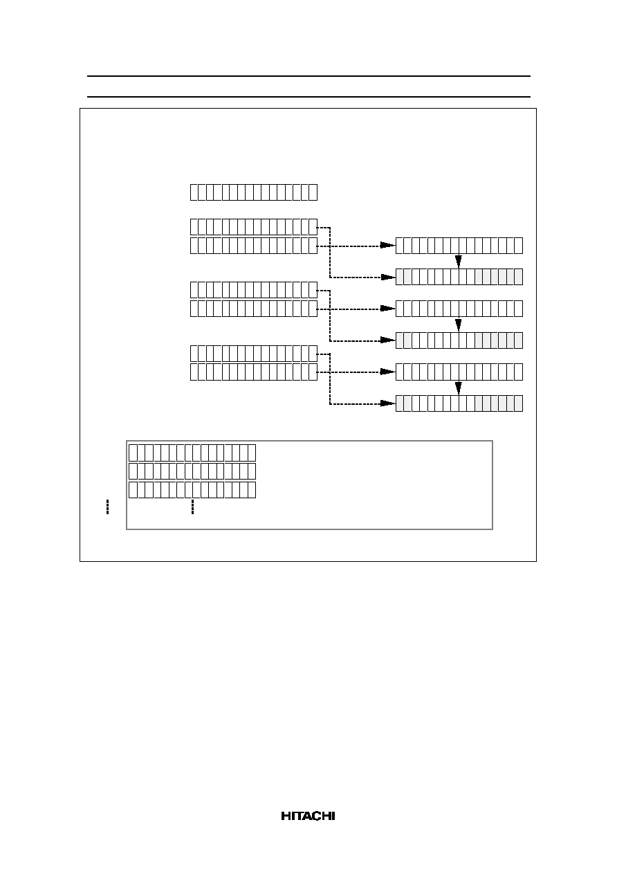
HD66750/1
47
WM0
WM15
1 1 0 0 0 0 0 0 0 0 1 1 1 1 1 1
DB0
DB15
1 0 1 1 1 1 0 0 0 1 1 0 0 0 0 1
1 1 0 0 0 0 1 1 1 0 0 0 1 1 0 0
0 1 1 1 0 1 0 0 0 0 0 1 1 1 1 1
1 0 0 1 1 0 0 1 0 1 0 0 0 0 1 1
0 0 0 0 1 1 1 1 0 0 0 0 0 0 0 0
0 0 0 0 1 1 1 0 1 1 1 0 0 1 1 0
000H
CGRAM
010H
020H
*
*
*
*
*
*
*
*
*
*
*
*
*
*
*
*
*
*
4-bit rotation
4-bit rotation
4-bit rotation
1 1 0 1 1 1 1 0 0 0 1 1 1
1 0 0
0 1 1 1 1 0 0 1 1 1 0 0 0
1 1 0
1 1 1 1 1 1 1 1 0 0 1 1 1
1 1 1
*
*
*
*
*
*
1 1 0 1 1 1 1
0
0 1 1 1 1 0 0
0
1 1 1 1 1 1 1
1
7F0H
1 0 1 1 1 1 0 0 0 1 1 0
0 0 0 1
1 1 0 0 0 0 1 1 1 0 0 0
1 1 0 0
0 1 1 1 0 1 0 0 0 0 0 1
1 1 1 1
000H
001H
Write data mask:
Write data (1):
Write data (2):
Write data (3):
Read data (1) + Write data (1)
Read data (1):
Read data (2):
Read data (3):
Logical operation (OR)
Logical operation (OR)
Logical operation (OR)
Read data (2) + Write data (2)
Read data (3) + Write data (3)
1) I/D = 1, AM1–0 = 01, LG1–0 = 01 (OR), RT2–0 = 010
2) WM15–0 = FC03H
3) AC = 000H
Operation Examples:
Notes: 1. The bit area data in the RAM indicated by '*' is not changed.
2. After writing to address 7F0H, the AC jumps to 001H.
Figure 30 Writing Operation of Read/Write Mode 2
6. Read/Write mode 3: AM1–0 = 10, LG1–0 = 01/10/11
This mode is used when the data is written with high speed by vertically shifting bits and by performing
logical operation with the original data. It can be also used to write the 16-bit data for two words into the
graphics RAM (CGRAM), develop the font pattern, or transfer the BiTBLT as a bit unit. This mode can
read the data during the same bus cycle as for the write operation since the read operation of the original
data does not latch the read data into the microcomputer and temporarily holds it in the read-data latch.
The
rot
a
ti
on func t
ion (R
T2–0) or wr it
e -dat
a m
as
k func t
ion (W M
15–0) ar e al
s
o ena bl
ed i
n t
hes
e
oper at i ons . Howe ver, al t hough t he wr it e -dat a m as k func t ion m as ks t he bi t pos i ti on s et wi t h t he wr it e -
data mask register (WM15–0) at the odd-times (such as the first or third) write, the function masks the bit
pos i ti on whi ch re ver se d t he s et t i ng val ue of t he wr it e -dat a m as k re gi st e r (W M 15–0) at t he eve n-t i m es
(s uc h as t he s ec ond or four th) wr it e . Af te r t he odd-t i m es wr it i ng, t he addr es s count e r (A C)
automatically increments by 1 (I/D = 1) or decrements by 1 (I/D = 0). After the even-times writing, the
AC aut om at i ca l ly i ncr em ent s or dec re me nt s by –1 + 16 (I /D = 1) or + 1 + 16 (I /D = 0). The AC
automatically jumps to the upper edge after it has reached the lower edge of the graphics RAM.
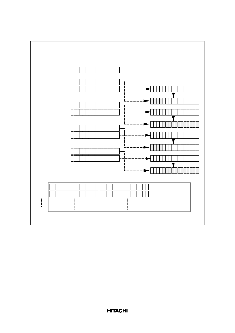
HD66750/1
48
WM0
WM15
1 1 1 1 0 0 0 0 0 0 0 0 0 0 0 0
DB0
DB15
1 1 1 1 1 1 0 0 0 0 0 1 1 0 0 0
1 1 1 1 1 1 0 0 0 0 0 1 1 0 0 0
0 0 0 0 0 1 1 1 0 0 0 0 1 1 1 1
000H
Write data (1), (2)
CGRAM
010H
Write data (3), (4)
*
0 0 0 0 0 1 1 1 0 0 0 0 1 1 1 1
1 1 1 1 1 1 0 0 0 0 0 1
1 0 0 0
1 1 1 1 1 1 0 0 0 0 0 1
1 0 0 0
0 0 0 0 0 1 1 1 0 0 0 0
1 1 1 1
0 0 0 0 0 1 1 1 0 0 0 0
1 1 1 1
*
*
*
*
*
*
*
*
*
*
*
*
*
*
*
*
*
*
*
*
*
*
*
*
*
*
*
*
*
*
*
000H
001H
7F0H
0 0 0 1 1 1 1 0 0 0 0 0 1 1 0 0
0 0 1 1 1 1 1 1 0 0 0 0 0 1 1 1
0 0 1 1 0 0 1 1 0 0 0 0 0 1 1 0
1 1 1 1 0 0 0 0 0 0 0 0 0 1 0 1
1 1 1 1 1 1 0 0 1 1 0 1
1 0 0 1
1 1 1 1 1 1 0 0 0 1 1 1
1 0 1 1
0 0 1 1 0 1 1 1 0 1 1 0
1 1 1 1
0 0 0 0 0 1 1 1 0 1 0 1
1 1 1 1
1 1 1 1 1 1 0 0 1 1 0 1
1 0 1 1
0 0 1 1 0 1 1 1 0 1 1 0
1 1 1 1
4-bit rotation
4-bit rotation
4-bit rotation
Write data mask:
Write data (1):
Write data (2):
Write data (3):
Read data (1):
Read data (2):
Read data (3):
Logical operation (OR)
Logical operation (OR)
Logical operation (OR)
1) I/D = 1, AM1–0 = 10, LG1–0 = 01, RT2–0 = 010
2) WM15–0 = 000FH
3) AC = 000H
Operation Examples:
Write data (4):
Read data (4):
4-bit rotation
Logical operation (OR)
Notes: 1. The bit area data in the RAM indicated by '*' is not changed.
2. After writing to address 7F0H, the AC jumps to 001H.
Figure 31 Writing Operation of Read/Write Mode 3
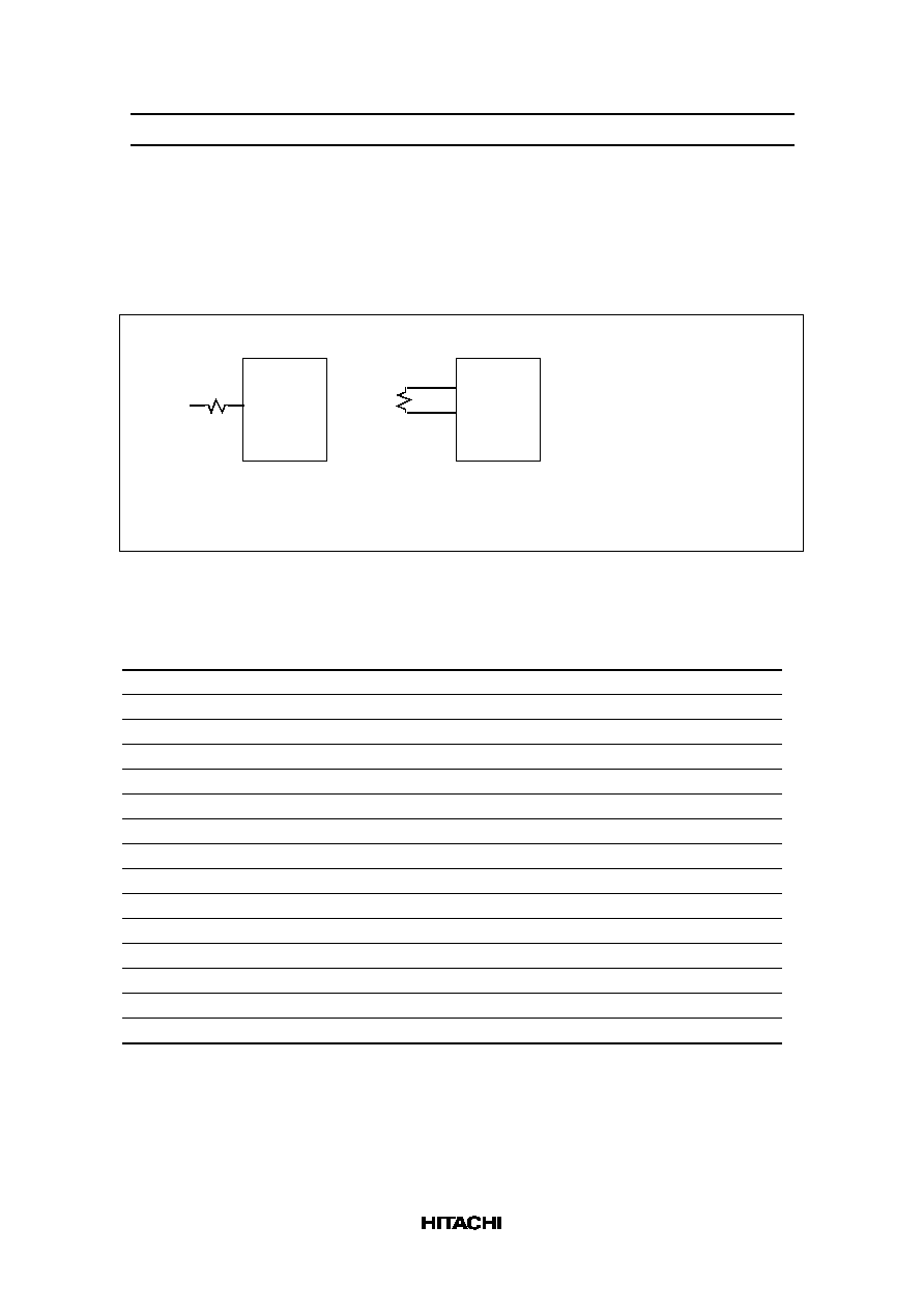
HD66750/1
49
Oscillation Circuit
The HD66750/1 can either be supplied with operating pulses externally (external clock mode) or oscillate
using an internal R-C oscillator with an external oscillator-resistor (external resistor oscillation mode).
Note that in R-C oscillation, the oscillation frequency is changed according to the internal capacitance
value, the external resistance value, or operating power-supply voltage.
1) External cloc k mode
2) External resistor oscillation mode
OSC1
OSC1
OSC2
Cloc k
(70 kHz)
Rf
The oscillator frequency can be
adjusted by oscillator resistor
(Rf). If Rf is increased or power
supply voltage is decreased, the
oscillation frequency dec reas es.
For the relationship between Rf
resistor value and oscillation
frequency, see the Elec tric
Characteristics Notes section.
HD66750/1
HD66750/1
Dumping resistance
(1.5 k
)
Figure 32 Oscillation Circuits
Table 18
Relationship between Liquid Crystal Drive Duty Ratio and Frame Frequency
LCD Duty
NL3–0 Set Value
Recommended
Drive Bias Value
Frame
Frequency
One-frame Clock
1/16
0001
1/6
70 Hz
1024
1/24
0010
1/6
70 Hz
1032
1/32
0011
1/6
70 Hz
1024
1/40
0100
1/7
69 Hz
1040
1/48
0101
1/8
71 Hz
1008
1/56
0110
1/8
71 Hz
1008
1/64
0111
1/9
70 Hz
1024
1/72
1000
1/9.5
71 Hz
1008
1/80
1001
1/10
69 Hz
1040
1/88
1010
1/10
68 Hz
1056
1/96
1011
1/10
68 Hz
1056
1/104
1100
1/11
69 Hz
1040
1/112
1101
1/11
71 Hz
1008
1/120
1110
1/11
67 Hz
1080
1/128
1111
1/11
70 Hz
1024
Note:
The frame frequency above is for 72-kHz operation and proportions the oscillation frequency (fosc).
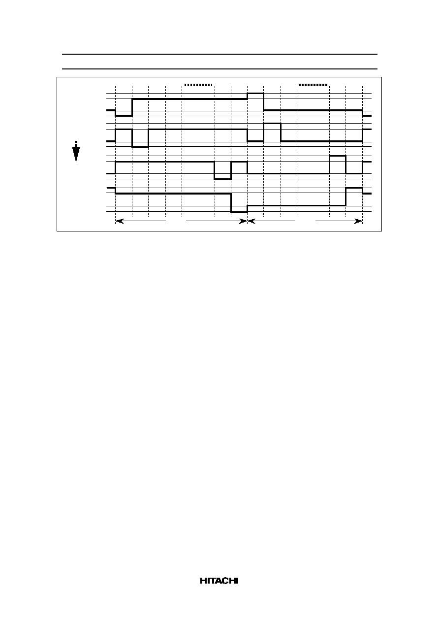
HD66750/1
50
1
2
3
4
127
128
1
2
3
127
128
V1
V2
V5
GND
COM1
V2
V5
GND
COM2
1 frame
1 frame
V1
V2
V5
GND
COM127
V1
V2
V5
GND
COM128
V1
Figure 33 LCD Drive Output Waveform (B-pattern AC Drive with 1/128 Multiplexing Duty Ratio)

HD66750/1
51
n-raster-row Reversed AC Drive
The HD66750/1 supports not only the LCD reversed AC drive in a one-frame unit (B-pattern waveform)
but also the n-raster-row reversed AC drive which alternates in an n-raster-row unit from one to 32 raster-
rows (C-pattern waveform). When a problem affecting display quality occurs, such as crosstalk at high-
duty driving of more than 1/64 duty, the n-raster-row reversed AC drive (C-pattern waveform) can improve
the quality. Determine the number of raster-rows n (NW bit set value + 1) for alternating after confirmation
of the display quality with the actual LCD panel. However, if the number of AC raster-rows is reduced, the
LCD alternating frequency becomes high. Because of this, the charge or discharge current is increased in
the LCD cells.
1 2 3 4 5 6 7 8 9 10 11 12 13
79 80 1 2 3 4 5 6 7 8 9 10 1112 13
79 80 1 2 3
B-pattern
waveform drive
• 1/80 duty
1 frame
1 frame
C-pattern
waveform drive
• 1/80 duty
• 11-raster-row
reversal
• Without EORs
C-pattern
waveform drive
• 1/80 duty
• 11-raster-row
reversal
• With EORs
Note: Specify the number of AC drive raster-rows and the necessity of EOR so that the DC bias is not generated for
the liquid crystal.
Figure 34 Example of an AC Signal under n-raster-row Reversed AC Drive

HD66750/1
52
Liquid Crystal Display Voltage Generator
When External Power Supply and Internal Operational Amplifiers are Used
To supply LCD drive voltage directly from the external power supply without using the internal booster,
circuits should be connected as shown in figure 35. Here, contrast can be adjusted by software through the
CT bits of the contrast adjustment register.
The HD66750/1 incorporates a voltage-follower operational amplifier for each V1 to V5 to reduce current
flowing through the internal bleeder-resistors, which generate different levels of liquid-crystal drive
voltages. Thus, potential difference between V
LCD
and V1 must be 0.1 V or higher, and that between V4 and
GND must be 1.4 V or higher. Note that the OPOFF pin must be grounded when using the operational
amplifiers. Place a capacitor of about 0.47
µ
F (B characteristics) between each internal operational
amplifier (V1OUT to V5OUT outputs) and GND and stabilize the output level of the operational amplifier.
Adjust the capacitance value of the stabilized capacitor after the LCD panel has been mounted and the
screen quality has been confirmed.
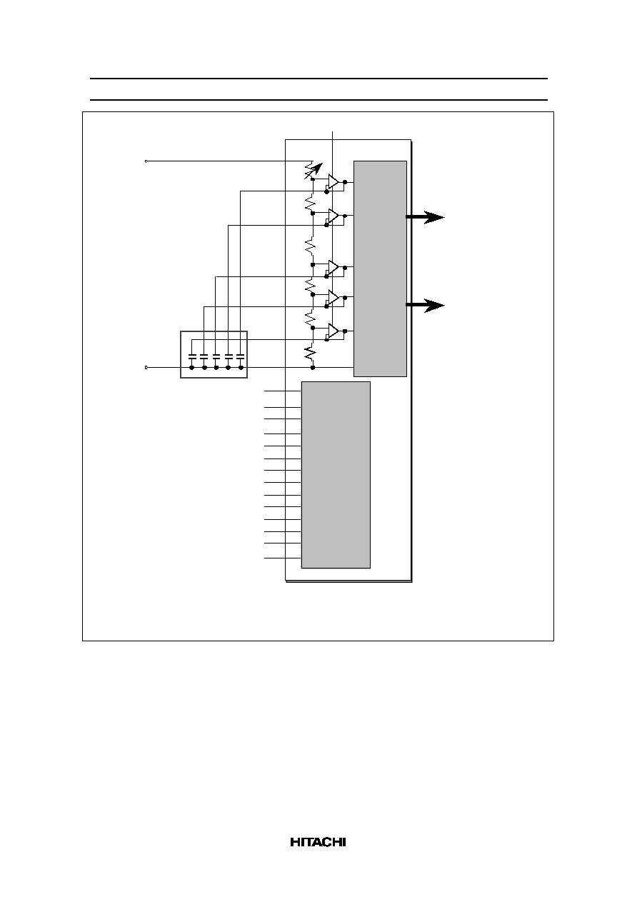
HD66750/1
53
C1+
V
LCD
V
LCD
V R
R
0
R
R
R
-
+
-
+
-
+
-
+
-
+
GND
O POFF = G ND
R
HD66750/1
V 1OUT
V 2OUT
V 3OUT
V 4OUT
V 5OUT
SEG1 to SEG128
CO M1 to CO M12
G ND
V ci
C1-
C2+
C2-
V LOUT
0.47
µ
F*
(B characteristics)
C3+
C3-
C4+
C4-
C5+
C5-
C6+
C6-
Note: A djust the capacitance value of the capacitor after the LCD p anel has b een mounted.
The capacitors connected to V 1OUT to V 5OUT/GND should b e more the V lcd voltage.
The voltage of these capacitors should b e determined with fluctuation of voltage.
B ooster
LCD
driver
V 1
V 3
V 4
V 2
V 5
GND
Figure 35 External Power Supply Circuit for LCD Drive Voltage Generation
When an Internal Booster and Internal Operational Amplifiers are Used
To supply LCD drive voltage using the internal booster, circuits should be connected as shown in figure 36.
Here, contrast can be adjusted through the CT bits of the contrast control instruction. Temperature can be
compensated either through the CT bits or by controlling the reference voltage for the booster (Vci pin)
using a thermistor.
Note that Vci is both a reference voltage and power supply for the booster. The reference voltage must
therefore be adjusted using an emitter-follower or a similar element so that sufficient current can be
supplied. In this case, Vci must be equal to or smaller than the V
CC
level.

HD66750/1
54
The HD66750/1 incorporates a voltage-follower operational amplifier for each of V1 to V5 to reduce
current flowing through the internal bleeder-resistors, which generate different liquid-crystal drive voltages.
Thus, potential difference between V
LCD
and V1 must be 0.1 V or higher, and that between V4 and GND
must be 1.4 V or higher. Note that the OPOFF pin must be grounded when using the operational amplifiers.
Place a capacitor of about 0.47
µ
F (B characteristics) between each internal operational amplifier (V1OUT
to V5OUT outputs) and GND and stabilize the output level of the operational amplifier. Adjust the
capacitance value of the stabilized capacitor after the LCD panel has been mounted and the screen quality
has been confirmed.
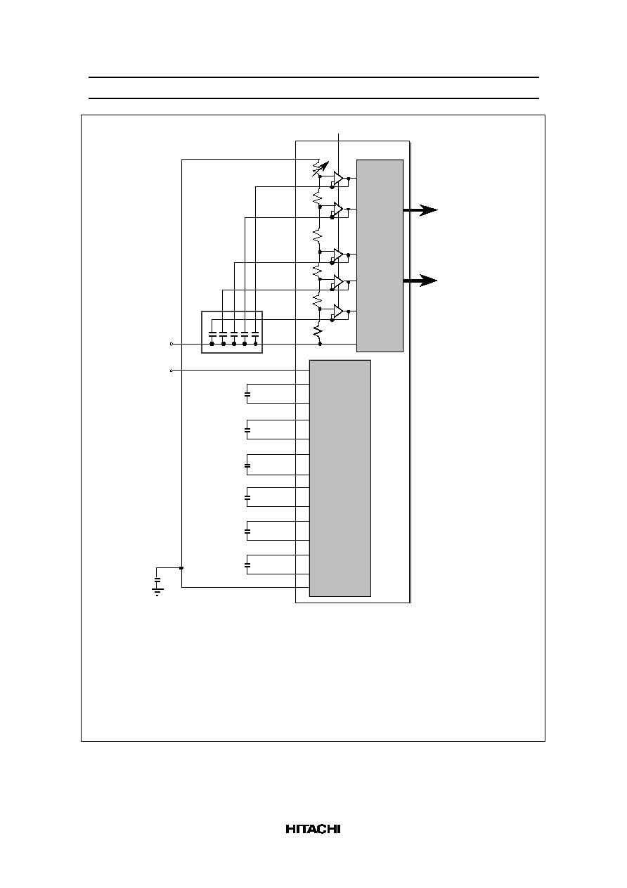
HD66750/1
55
V
LCD
VR
R
0
R
R
R
-
+
-
+
-
+
-
+
-
+
GND
C1+
C1-
Vci
VLOU T
GND
C2+
C2-
(+)
B oo ste r
O PO FF = G ND
R
HD6 6750/1
V1OUT
V2OUT
V3OUT
V4OUT
V5OUT
LCD
driver
SEG 1 to SEG 128
CO M 1 to CO M128
V1
V3
V4
V2
V5
G N D
0.47
µ
F*
(B characteristics )
GND
Vci
C3+
C3-
C4+
C4-
1
µ
F
(B Charac-
teris tic s)
Not es :1. The reference voltage input (Vci) mus t be adjus ted s o that the outp ut voltage after boos ting will not exc
the ab solut e maxi mum rating f or the liquid-crystal power s up ply v oltage (16.5 V) .
2. Vci is both a reference v oltage and p ow er supp ly for the boost er; connect it to Vcc directly or comb ine it
with a t rans istor so t hat suff icient current can b e obt ained.
3. Polariz ed capacitors m us t be connected correctly.
4. Circuits for temp erature comp ensat ion s hould b e b as ed on the sampl e circuits in figure 37.
5. Adjust the capacitance value of the stab ilized capacitor aft er the LCD panel has been m ounted.
6. The cap acitors connected to C3+/ C3– and C 6+ /C 6– should three times or more the Vci v oltage.
7. The cap acitors connected to C1+/ C1–, C2+/ C2–, C 4+ /C 4– and C5+/ C5– s hould b e more the V ci volta
8. The cap acitors connected to VLOU T/GND and V 1OU T to V5OUT/ GND should be more the N times Vci
v oltage. (N: b oost ing factor)
9. The v oltage of these capacitors should be determi ned with fluctuation of voltage.
C5+
C5-
C6+
C6-
(+)
1
µ
F
(B Charac-
teri s ti cs )
(+)
1
µ
F
(B Charac-
teri s ti cs )
(+)
1
µ
F
(B Charac -
teristi c s)
(+)
1
µ
F
(B Charac -
teristi c s)
(+)
1
µ
F
(B Charac -
teristi c s)
(+ )
1
µ
F
(B Charac-
teri s tics )
Figure 36 Internal Booster for LCD Drive Voltage Generation
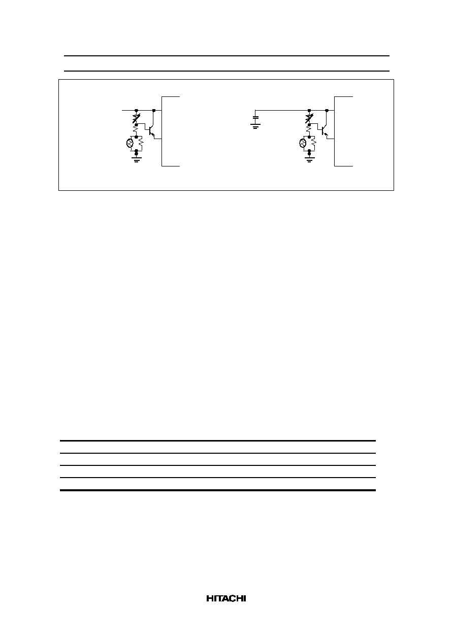
HD66750/1
56
V cc
Thermistor
GND
Tr
V cc
V ci
HD66750/1
1
µ
F
(B charac-teristics)
Thermistor
GND
Tr
V cc
V ci
HD66750/1
GND
(+)
(Examp le 1)
(Examp le 2)
Figure 37 Temperature Compensation Circuits
Switching the Boosting Factor
Instruction bits (BT1/0 bits) can optionally select the boosting factor of the internal booster. According to
the display status, power consumption can be reduced by changing the LCD drive duty and the LCD drive
bias, and by controlling the boosting factor for the minimum requirements. For details, see the Partial-
display-on Function section.
Because of the maximum boosting factor, external capacitors need to be connected. For example, when the
maximum boosting is six times or five times, capacitors between C6+ and C6– or between C5+ and C5– are
needed as well, as in the case of the seven-times boosting. When the boosting is two-times boosting,
capacitors between C1+ and C1– or between C4+ and C4– are not needed.
Place a capacitor with a voltage of three times or more the Vci-GND voltage between C6+ and C6– and
between C3+ and C3–, and a capacitor with a voltage larger than the Vci-GND voltage between C1+ and
C1–, C2+ and C2–, C4+ and C4–, and C5+ and C5–.
Place a capacitor with a voltage of N times theVci-GND voltage between VLOUT and GND. (N: boosting
factor)
Note that each capacitors with a voltage should be determined with a voltage fluctuation.
Table 19
VLOUT Output Status
BT1
BT0
VLOUT Output Status
0
0
Two-times boosting output
0
1
Five-times boosting output
1
0
Six-times boosting output
1
1
Seven-times boosting output
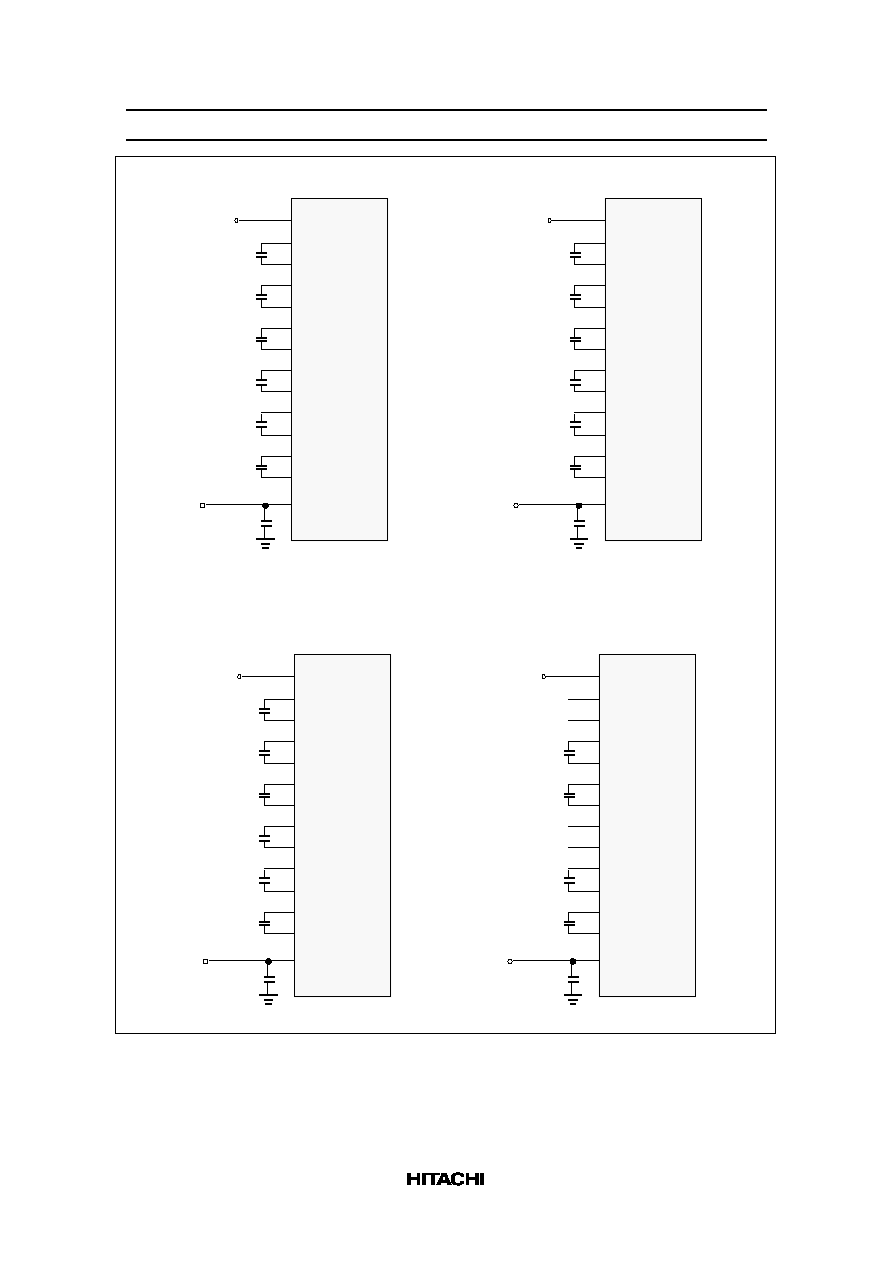
HD66750/1
57
ii) Maximum six-times boosting
iii) Maximum five-times boosting
iv) Maximum two-times boosting
C1+
C1-
Vci
VLOUT
GND
C2+
C2-
Vci
C3+
C3-
i) Maximum seven-times boosting
C4+
C4-
C5+
C5-
C6+
C6-
(+)
1
µ
F
(B Charac-
teristics)
(+)
1
µ
F
(B Charac-
teristics)
(+)
1
µ
F
( B Char ac-
ter istics)
(+)
1
µ
F
( B Char ac-
ter istics)
(+)
1
µ
F
(B Charac-
teristics)
(+)
1
µ
F
( B Char ac-
ter istics)
(+)
1
µ
F
( B Char ac-
ter istics)
C1+
C1-
Vci
VLOUT
GND
C2+
C2-
Vci
C3+
C3-
C4+
C4-
C5+
C5-
C6+
C6-
(+)
1
µ
F
(B Charac-
teristics)
(+)
1
µ
F
(B Charac-
teristics)
(+)
1
µ
F
(B Charac-
teristics)
(+)
1
µ
F
(B Charac-
teristics)
(+)
1
µ
F
( B Char ac-
ter istics)
(+)
1
µ
F
(B Charac-
teristics)
(+)
1
µ
F
(B Charac-
teristics)
C1+
C1-
Vci
VLOUT
GND
C2+
C2-
Vci
C3+
C3-
C4+
C4-
C5+
C5-
C6+
C6-
(+)
1
µ
F
(B Charac-
teristics)
(+)
1
µ
F
(B Charac-
teristics)
(+)
1
µ
F
( B Char ac-
ter istics)
(+)
1
µ
F
( B Char ac-
ter istics)
(+)
1
µ
F
(B Charac-
teristics)
(+)
1
µ
F
( B Char ac-
ter istics)
(+)
1
µ
F
( B Char ac-
ter istics)
C1+
C1-
Vci
VLOUT
GND
C2+
C2-
Vci
C3+
C3-
C4+
C4-
C5+
C5-
C6+
C6-
(+)
1
µ
F
(B Charac-
teristics)
(+)
1
µ
F
( B Char ac-
ter istics)
(+)
1
µ
F
(B Charac-
teristics)
(+)
1
µ
F
( B Char ac-
ter istics)
(+)
1
µ
F
( B Char ac-
ter istics)
Figure 38 Booster Output Factor Switching
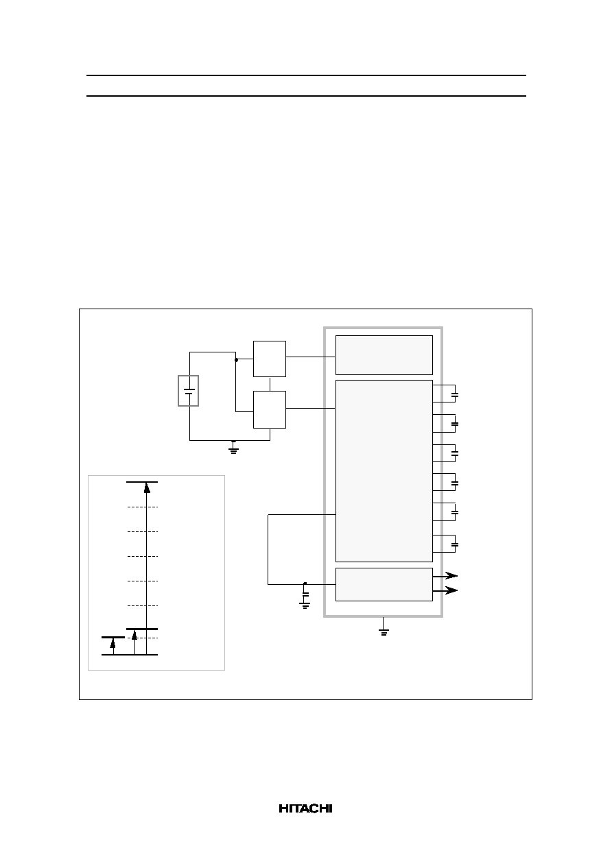
HD66750/1
58
Example of Power-supply Voltage Generator for More Than Seven-times Boosting Output
The HD66750/1 incorporates a booster for up to seven-times boosting. However, the LCD drive voltage
(VLCD) will not be enough for seven-times boosting from Vcc when the power-supply voltage of Vcc is
low or when the LCD drive voltage is high for the high-contrast LCD display. In this case, the reference
voltage (Vci) for boosting can be set higher than the power-supply voltage of Vcc.
When the boosting factor is high, the current driving ability is lowered and insufficient display quality may
result. In this case, the boosting ability can be improved by decreasing the boosting factor as shown in the
booster in figure 39.
Set the Vci input voltage for the booster to 3.6 V or less within the range of Vcc + 1.0 V. Control the Vci
voltage so that the boosting output voltage (VLOUT) should be less than the absolute maximum ratings
(16.5 V).
C1+
C1 –
Vci
VLOUT
GND
C2+
C2 –
B ooster
C3+
C3 –
C4+
C4 –
LCD driver
SEG1 to SEG128
COM1 t o COM128
Regu-
lator
(2)
Vci
Regu-
lator
(1)
Vcc
L ogic circuit
1.8 V
2.2 V
VLCD
GND
GND
GND
2.2 V x 7 = 15.4 V
B attery
3.6 V
GND (= 0 V)
Vcc (= 1. 8 V)
Vci (= 2. 2 V)
HD66750/ 1
VLCD (= 15.4 V)
C5+
C5 –
C6+
C6 –
Note: I n pract ice, t he LCD drive current lowers
t he volt age in t he boost ing out put volt age.
( +)
1
µ
F
(B Charac-
teri s tics )
( +)
1
µ
F
(B Chara c-
teristic s)
( +)
1
µ
F
(B Chara c-
teristic s)
( +)
1
µ
F
(B Ch arac-
teristi cs)
( +)
1
µ
F
(B Ch arac-
teristi cs)
( +)
1
µ
F
(B Ch arac-
teristi cs)
( +)
1
µ
F
(B Charac-
teri s tics )
Figure 39 Usage Example of Booster at Vci > Vcc
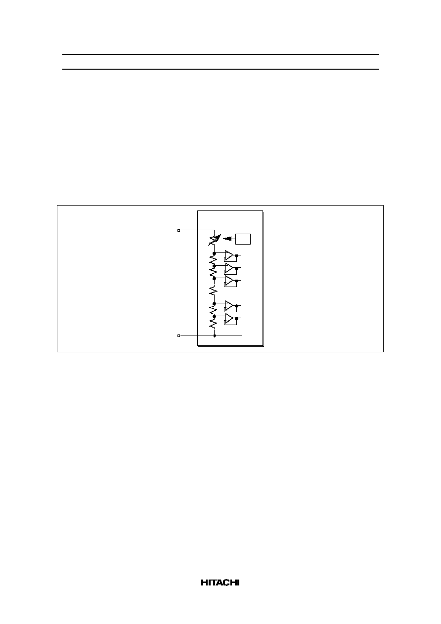
HD66750/1
59
Contrast Adjuster
Software can adjust 64-step contrast for an LCD by varying the liquid-crystal drive voltage (potential
difference between V
LCD
and V1) through the CT bits of the contrast adjustment register (electron volume
function). The value of a variable resistor between V
LCD
and V1 (VR) can be precisely adjusted in a 0.05 x
R unit within a range from 0.05 x R through 3.20 x R, where R is a reference resistance obtained by dividing
the total resistance.
The HD66750/1 incorporates a voltage-follower operational amplifier for each of V1 to V5 to reduce
current flowing through the internal bleeder resistors, which generate different liquid-crystal drive voltages.
Thus, CT5-0 bits must be adjusted so that potential difference between V
LCD
and V1 is 0.1 V or higher and
that between V4 and GND is 1.4 V or higher when liquid-crystal drives, particularly when the VR is small.
VLCD
VR
R
R
R0
R
R
-
+
-
+
-
+
-
+
-
+
GND
HD66750/1
CT
V1
V2
V3
V4
V5
GND
Figure 40 Contrast Adjuster
HD66750/1
60
Table 20
Contrast Adjustment Bits (CT) and Variable Resistor Values
0
CT3
0
CT2
0
CT1
0
CT0
3.20 x R
CT Set Value
Variable Resistor
Value (VR)
0
0
0
1
3.15 x R
0
0
1
0
3.10 x R
0
0
1
1
3.05 x R
0
1
0
0
3.00 x R
0
1
0
1
2.95 x R
0
1
1
0
2.90 x R
0
1
1
1
2.85 x R
0
CT4
0
0
0
0
0
0
0
1
0
0
1
2.75 x R
0
1
0
1
0
2.70 x R
0
Potential Difference
between V1 and GND
Display Color
(Small)
(Large)
(Light)
(Deep)
1
0
1
2.65 x R
0
1
1
0
0
2.60 x R
0
1
1
1
1
1.65 x R
1
0
0
0
0
1.60 x R
0
0
0
0
1
1.55 x R
0
0
0
1
0
1.50 x R
0
0
0
1
1
1.45 x R
0
0
1
0
0
1.40 x R
0
0
1
0
1
1.35 x R
0
0
1
1
0
1.30 x R
0
0
1
1
1
1.25 x R
0
1
0
0
0
1.20 x R
0
1
0
0
1
1.15x R
1
1
1
0
0
0.20 x R
1
1
1
0
1
0.15 x R
1
1
1
1
0
0.10 x R
1
1
1
1
1
0.05 x R
1
1
0
0
0
2.80 x R
0
1
0
CT5
0
0
0
0
0
0
0
0
0
0
0
0
1
1
1
1
1
1
1
1
1
1
1
1
1
1
0
HD66750/1
61
Liquid-crystal-display Drive-bias Selector
An optimum liquid-crystal-display bias value can be selected using the BS2-0 bits, according to the liquid
crystal drive duty ratio setting (NL3-0 bits). The liquid-crystal-display drive duty ratio and bias value can
be displayed while switching software applications to match the LCD panel display status. The optimum
bias value calculated using the following expression is a logical optimum value. Driving by using a lower
value than the optimum bias value provides lower logical contrast and lower liquid-crystal-display voltage
(the potential difference between V1 and GND), which results in better image quality. When the liquid-
crystal-display voltage is insufficient even if a seven-times booster is used, when the boosting driving
ability is lowered by setting a high factor for the booster, or when the output voltage is lowered because the
battery life has been reached, the display can be made easier to see by lowering the liquid-crystal-display
bias.
The liquid crystal display can be adjusted by using the contrast adjustment register (CT5-0 bits) and
selecting the booster output level (BT1/0 bits).
Optimum bias value for 1/N duty ratio drive voltage =
1
N + 1
Table 21
Optimum Drive Bias Values
LCD drive
duty ratio
1/128
1/120
1/112
1/104
1/96
1/88
1/80
1/72
1/64
1/32
1/24
1/16
(NL3-0 set
value)
1111
1110
1101
1100
1011
1010
1001
1000
0111
0100
0011
0010
Optimum
drive bias
value
1/11
1/11
1/11
1/11
1/10
1/10
1/10
1/9
1/9
1/6
1/6
1/5
(BS2-0 set
value)
000
000
000
000
001
001
001
010
010
101
101
100

HD66750/1
62
VR
V1
V2
V3
V4
V5
R
R
7R
R
R
V1
V2
V3,V4
V5
GND
R
R
R
R
i) 1/ 11 bias
(BS2–0 = 000)
vi) 1/ 4 bias
(BS2–0 = 111)
GND
VR
VLC D
VLCD
N ote: R = Reference resistor
VR
V1
V2
V3
V4
V5
R
R
6R
R
R
ii) 1/ 10 bias
(BS2–0 = 001)
VLCD
VR
V1
V2
V3
V4
V5
R
R
5R
R
R
iii) 1/ 9 bias
(BS2–0 = 010)
VLCD
VR
V1
V2
V3
V4
V5
R
R
4R
R
R
iv) 1/ 8 bias
(BS2–0 = 011)
VLCD
VR
GND
V1
V2
V3
V4
V5
R
R
3R
R
R
v) 1/7 bias
(BS2–0 = 100)
VLCD
GND
GN D
GND
GND
GND
GND
GND
GN D
GND
VR
GND
V1
V2
V3
V4
V5
R
R
2R
R
R
v) 1/6 bias
(BS2–0 = 101)
VLCD
GND
VR
GND
V1
V2
V3
V4
V5
R
R
R
R
R
v) 1/5 bias
(BS2–0 = 110)
VLCD
GND
Figure 41 Liquid Crystal Display Drive Bias Circuit
HD66750/1
63
Table 22
Contrast Adjustment per Bias Drive Voltage
10 x R + VR
10 x R
x (V
LCD
- GND)
0.757 x (V
LCD
-GND)
V
DR
0.995 x (V
LCD
-GND)
1.4 [V]
0.1 [V]
10 x R + VR
VR
x (V
LCD
-GND)
10 x R + VR
2 x R
x (V
LCD
-GND)
5 x R + VR
5 x R
x (V
LCD
- GND)
0.610 x (V
LCD
-GND )
V
DR
0.990 x (V
LCD
-GND)
1.4 [V]
0.1 [V]
5 x R + VR
VR
x (V
LCD
-GND )
5 x R + VR
2 x R
x (V
LCD
-GND )
4 x R + VR
4 x R
x (V
LCD
- GND)
0.556 x (V
LCD
-GND)
V
DR
0.988 x (V
LCD
-GND)
1.4 [V]
0.1 [V]
4 x R + VR
VR
x (V
LCD
-GND)
4 x R + VR
2 x R
x (V
LCD
-GND)
9 x R + VR
9 x R
x (V
LCD
- GND)
0.737 x (V
LCD
-GND)
V
DR
0.994 x (V
LCD
-GND)
1.4 [V]
0.1 [V]
9 x R + VR
VR
x (V
LCD
-GND)
9 x R + VR
2 x R
x (V
LCD
-GND)
11 x R + VR
11 x R
x (V
LCD
- GND)
0.775 x (V
LCD
-GND)
V
DR
0.995 x (V
LCD
-GND)
1.4 [V]
0.1 [V]
VR
x (V
LCD
-GND)
11 x R + VR
2 x R
x (V
LCD
-GND)
11 x R + VR
Bias
LCD drive voltage: V
DR
Contrast adjustment range
1/11
bias
drive
1/10
bias
drive
1/9
bias
drive
1/5
bias
drive
1/4
bias
drive
- LCD drive voltage
adjustment range
- Limit of potential
difference between V4 and GND
- Limit if potential
difference between VLCD and V1
:
:
:
- LCD drive voltage
adjustment range
- Limit of potential
difference between V4 and GND
- Limit if potential
difference between VLCD and V1
:
:
:
8 x R + VR
8 x R
x (V
LCD
- GND)
0.714 x (V
LCD
-GND)
V
DR
0.993 x (V
LCD
-GND)
1.4 [V]
0.1 [V]
8 x R + VR
VR
x (V
LCD
-GND)
8 x R + VR
2 x R
x (V
LCD
-GND)
1/8
bias
drive
- LCD drive voltage
adjustment range
- Limit of potential
difference between V4 and GND
- Limit if potential
difference between VLCD and V1
:
:
:
6 x R + VR
6 x R
x (V
LCD
- GND)
0.652 x (V
LCD
-GND)
V
DR
0.992 x (V
LCD
-GND)
1.4 [V]
0.1 [V]
VR
x (V
LCD
-GND)
6 x R + VR
6 x R + VR
2 x R
x (V
LCD
-GND)
7 x R + VR
7 x R
x (V
LCD
- GND)
0.686 x (V
LCD
-GND)
V
DR
0.993 x (V
LCD
-GND)
1.4 [V]
0.1 [V]
VR
x (V
LCD
-GND)
7 x R + VR
2 x R
x (V
LCD
-GND)
7 x R + VR
1/7
bias
drive
1/6
bias
drive
- LCD drive voltage
adjustment range
- Limit of potential
difference between V4 and GND
- Limit if potential
difference between VLCD and V1
:
:
:
- LCD drive voltage
adjustment range
- Limit of potential
difference between V4 and GND
- Limit if potential
difference between VLCD and V1
:
:
:
- LCD drive voltage
adjustment range
- Limit of potential
difference between V4 and GND
- Limit if potential
difference between VLCD and V1
:
:
:
- LCD drive voltage
adjustment range
- Limit of potential
difference between V4 and GND
- Limit if potential
difference between VLCD and V1
:
:
:
- LCD drive voltage
adjustment range
- Limit of potential
difference between V4 and GND
- Limit if potential
difference between VLCD and V1
:
:
:

HD66750/1
64
Four-grayscale Display Function
The HD66750/1 supports the four-grayscale monochrome display function. The four-grayscale
monochrome display is used for the display data of the two-bit pixel set sent to the CGRAM. There are four
grayscale levels: always unlit, weak middle level, strong middle level, and always lit. In the weak
middle-level grayscale display, the GS bit can select the 1/3 or 1/2 level.
The frame rate control (FRC) method is used for grayscale control.
Table 23
Relationships between the CGRAM Data and the Display Contents
Upper Bit
Lower Bit
Liquid Crystal Display
0
0
Non-selected (unlit)
0
1
GS = 0: 1/3-level grayscale (one frame lit during a three-frame period)
GS = 1: 1/2-level grayscale (one frame lit during a two-frame period)
1
0
2/3-level grayscale (two frames lit during a three-frame period)
1
1
Selected (lit)
Note:
Upper bits: DB15, DB13, DB11, DB9, DB7, DB5, DB3, and DB1
Lower bits: DB14, DB12, DB10, DB8, DB6, DB4, DB2, and DB0
0 0 1 0 0 1 1 1 1 1 0 1 1 0 0 0
0 0 0 0 1 0 1 0 0 1 0 1 1 1 1 1
CGRAM
Grayscal e
c ontrol circuit
L SB
DB0
MSB
DB15
LSB
DB0
MSB
DB15
LCD panel display
Figure 42 Four-grayscale Monochrome Display

Window Cursor Display Function
The HD66750/1 displays the window cursor by specifying a window area. The horizontal display position of the
window cursor is specified with the horizontal cursor position register (HS6–0 to HE6–0), and the vertical display
position is specified with the vertical cursor position register (VS6–0 or VE6–0). In these display position setting
registers, ensure that HS6–0
HE6–0 and VS6–0
VE6–0. If these relationships are not satisfied, normal display
cannot be attained. In addition, if the setting is VS6–0 = VE6–0 = 00H, a cursor is displayed on a raster-row at the
most-upper edge of the screen.
This window cursor can automatically display the hardware-supported block cursor, highlight window, or menu
bar. The CM1–0 bits select the following four displays in each window cursor:
1. White-blink cursor (CM1–0 = 00): Alternately blinks between the normal display and an all-white (unlit)
display
2. Black-blink cursor (CM1–0 = 01): Alternately blinks between the normal display and an all-black (all lit)
display
3. Black-and-white reversed cursor (CM1-0 = 10): Black-and-white-reversed normal display (no blinking)
4. Black-and-white-reversed blink cursor (CM1–0 = 11): Alternately blinks between the normal display and a
black-and-white-reversed display
The above blinking display is switched in a 32-frame unit.
In vertical scrolling, note that this window cursor does not automatically move vertically.
Figure 43 White Blink Cursor Display
VS+1 =>
VE+1 =>
VS+1 =>
VE+1 =>
HS+1
HE+1
HS+1
HE+1
Blink
display
HD66750/1
HITACHI
65

HD66750/1
HITACHI
66
VS+1 =>
VE+1 =>
VS+1 =>
VE+1 =>
HS+1 HE+1
HS+1 HE+1
Blink
display
Figure 44 Black Blink Cursor Display
VS+1 =>
VE+1 =>
HS+1
HE+1
Figure 45 Black-and-white Reversed Cursor Display
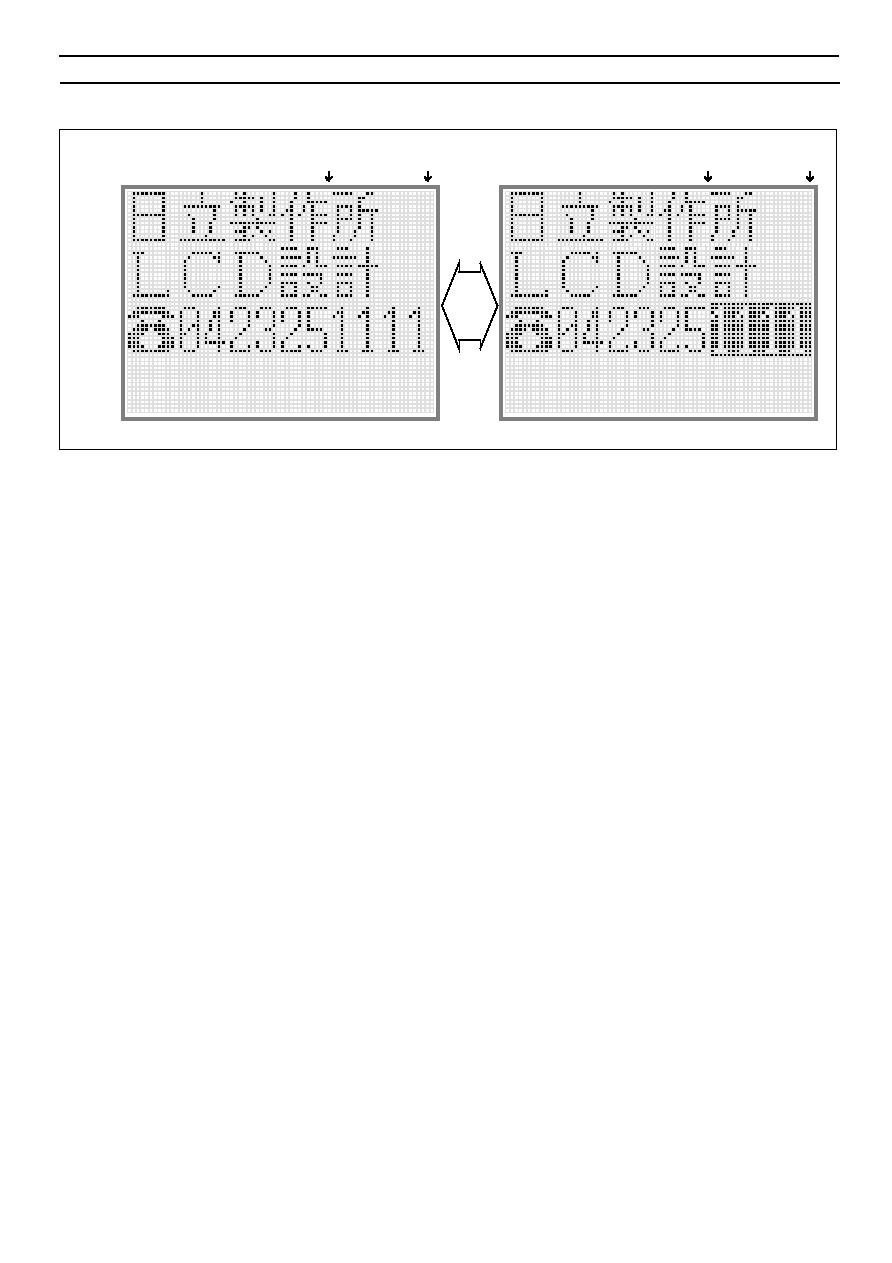
HD66750/1
HITACHI
67
Figure 46 Black-and-white Reversed Blink Cursor Display
VS+1 =>
VE+1 =>
HS+1
HE+1
HS+1
HE+1
Blink
display

HD66750/1
68
Vertical Smooth Scroll Display
The HD66750/1 can scroll the graphics display vertically in units of raster-rows. The data storage capacity
of the CGRAM is 128 raster-rows. Continuous smooth vertical scrolling is achieved by writing display data
into a raster-row area that is not being used for display. After the 128th raster-row is displayed, the first
raster-row is displayed again. Using the status read, the user can check the display raster-rows (L6-0) that
are currently driving the LCD, and flicker can be eliminated by writing the display data in the CGRAM
while the LCD is not driven.
Additionally, when display areas of a graphics icon such as a pictogram or a menu bar are partially fixed-
displayed, the remaining areas can be displayed. For details, see the Partial Smooth Scroll Display Function
section.
Specifically, this function is controlled by incrementing or decrementing the value in the display-start
raster-row bits (SL6-0) by 1. For example, to smoothly scroll up, increment display-start raster-row bits
(SL6-0) by 1 from 0000000 to 1111111 to scroll 128 raster-rows.
Note that the vertical double-height display or window cursor display is not automatically changed in
synchronization with the vertical scrolling.
When the response speed of the liquid crystal is low or when high-speed scrolling is needed, two- to four-
raster-row scrolling is recommended.
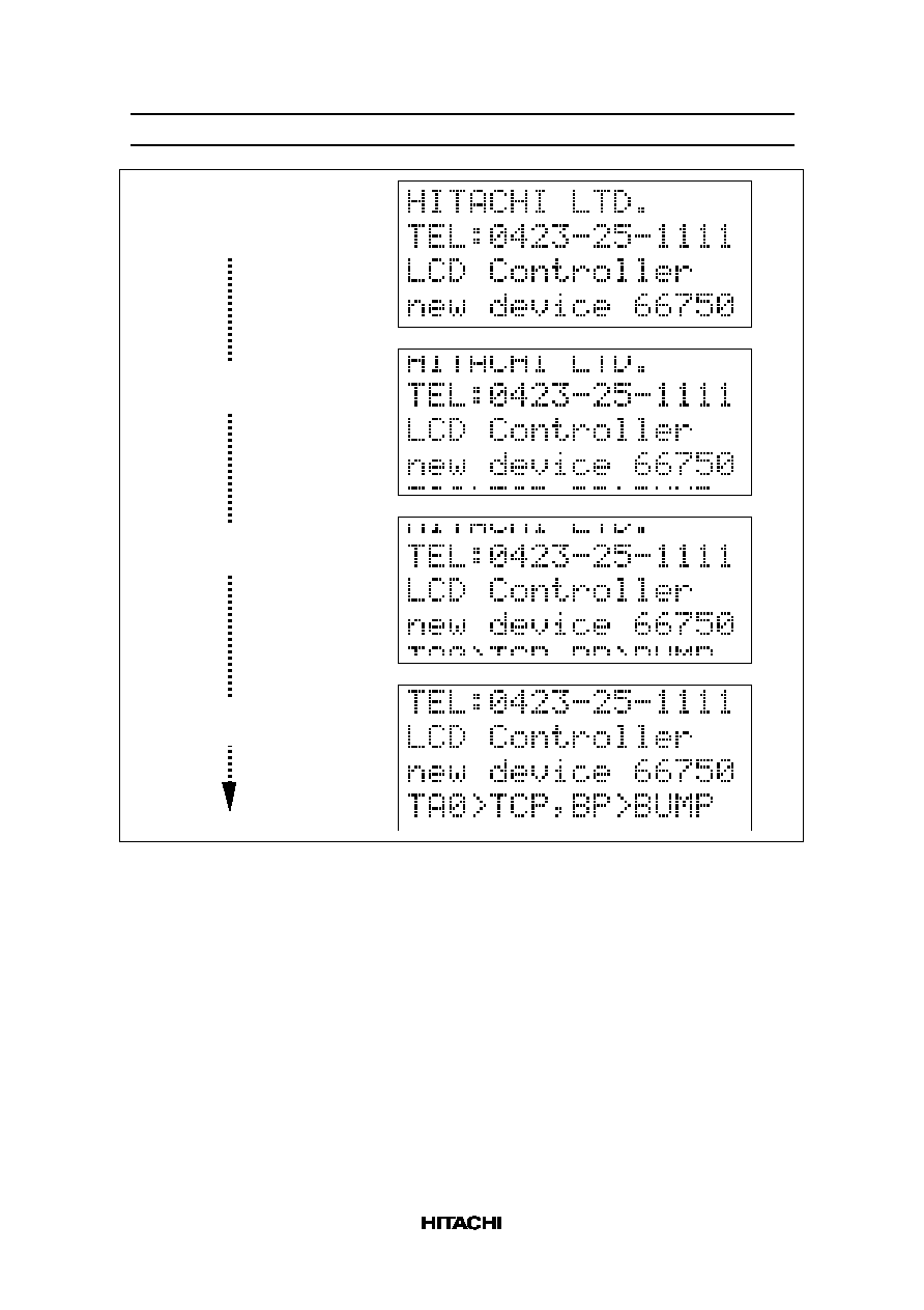
HD66750/1
69
1) Not scrolled
• SL6 to 0 = 0000000
2) Two raster-rows scrolled up
• SL6 to 0 = 0000010
3) Four raster-rows scrolled up
• SL6 to 0 = 0000100
4) Eight raster-rows scrolled up
• SL6 to 0 = 0001000
Figure 47 Vertical Smooth Scroll

HD66750/1
70
Partial Smooth Scroll Display Function
The HD66750/1 can partially fixed-display the areas of a graphics icon such as a pictogram or a menu bar,
and perform vertical smooth scrolling of the remaining bit-map areas. Since the PS1 to PS0 bits are not used
for smooth scrolling of the upper first to 24th display raster-rows but are used for fixed-display, pictograms
can be placed on the screen. This function can largely control the rewrite frequencies of the bit-map data
during smooth scrolling and reduce the software load of the MPU.
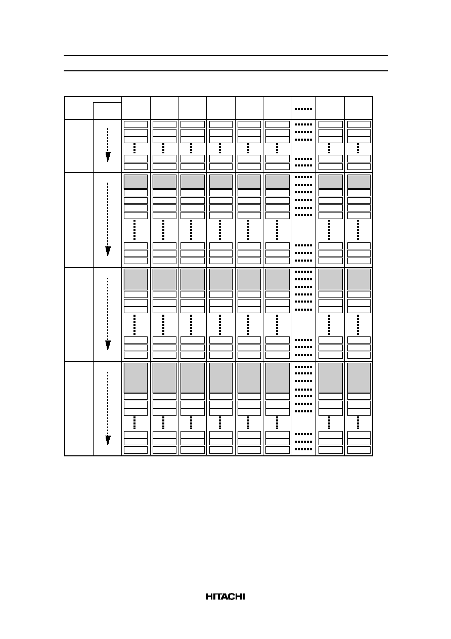
HD66750/1
71
Table 24 Bit Setting and Display Lines
Not es: 1. The shadow raster-rows above are fixed-displayed. They do not depend on the setting values of the SL6
to 0 bits.
2. The SL6 to 0 bits specify the next first scroll display rast er-row of the fixed-displayed rast er-rows.
1st r aster- row
2nd raster-row
3rd raster -row
119th raster-r ow
120th raster -row
PS1 t o 0
= 00
SL6 to 0
= 00H
2 nd raster -row
3rd raster-r ow
4th raster-row
121th raster-row
120th raster-row
SL6 to 0
= 01H
SL6 to 0
= 02H
COM1
COM120
121th raster-row
122th raster-row
3rd raster-r ow
4th raster-r ow
5th raster-r ow
1st to 8th
rast er-rows
1st r aster- row
2nd raster-row
3rd raster -row
4th raster- row
110 th raster-row
PS1 t o 0
= 01
2 nd raster -row
3rd raster-r ow
4th raster-row
5th raster-row
111th raster -row
112th raster -row
3rd raster-row
4th raster-row
5th raster-row
6th raster-row
1st raster-row
2nd r aster- row
3rd raster-row
PS1 to 0
= 10
3rd raster-r ow
4th raster-row
103th raster-row
4th raster-row
5th raster-row
104th raster-row
1st r aster- row
2nd raster-row
PS1 t o 0
= 11
2nd raster-r ow
3rd raster-row
97th raster-row
98th raster-r ow
3rd r aster- row
4th raster-r ow
102th raster-row
2 nd raster -row
SL6 t o 0
= 04H
123th raster-row
124th raster-row
5th raster-row
6th raster-row
7th raster-row
5th raster-row
6th raster-row
7th raster-row
8th raster-row
5th raster-row
6th raster-row
7th raster-row
5th raster-row
6th raster-row
100th raster-row
114th raster-row
SL6 to 0
= 07H
126th raster-row
127th raster-row
8th raster-row
9th raster-row
10th raster-row
117th raster-row
8th r aster- row
9th r aster- row
1 0th r aster- row
11th raster-row
110th raster -row
111th raster-r ow
8th raster-row
9th raster-row
10th raster-row
103th raster-row
8th raster-row
9th raster-row
SL6 to 0
= 7FH
3rd raster-row
108th raster-row
96th raster -row
Bit
Set ting
COM
Position
94th raster -row
96th raster-r ow
98th raster-row
101th raster-row
95th raster-row
95th raster -row
97th raster-r ow
99th raster-row
102th raster-row
96th raster-row
111th raster-row
112th raster-row
113th raster -row
115th raster-row
118th raster-row
112 th raster-row
113th raster-row
114 th raster-row
116th raster-row
119th raster-row
109th raster-row
106th raster-row
107th raster-row
104th raster-row
105th raster-row
103th raster-row
105th raster-row
106th raster-row
104th raster-row
SL6 to 0
= 7EH
COM1
COM120
COM1
COM120
COM1
COM120
117th raster -row
118th raster -row
127th raster-row
128th raster-row
1st raster-row
118th raster -row
119th raster -row
128th raster-row
1st raster-row
2rd raster-row
116th r aster- row
127th raster-row
128th raster-row
9th raster-row
10th raster-row
117th r aster- row
118th r aster- row
117th raster-r ow
128th raster -row
9th raster -row
1 0th raster -row
11th raster-r ow
118th raster-r ow
119th raster-r ow
117th raster -row
118th raster -row
127th raster-row
128th raster-row
17th raster-row
116th raster -row
118th raster-row
119th raster-row
128th raster-row
17th raster-row
18th raster-row
117th raster-row
SL6 to 0
= 08H
127th r aster- row
128th r aster- row
9th r aster- row
10th r aster- row
11th raster-r ow
118th r aster- row
9th raster-row
10th raster-row
11th raster -row
12th raster-row
111th raster-r ow
112th r aster- row
9th raster-row
10th raster-row
11th raster -row
104th r aster- row
9th raster-r ow
10th r aster- row
102th r aster- row
103th r aster- row
119th r aster- row
120th raster-row
110th r aster- row
118th r aster- row
127th raster -row
128th raster -row
116th r aster- row
117th r aster- row
119th raster-r ow
128th raster -row
2 5th raster -row
117th raster-r ow
118th raster-r ow
3rd raster -row
4th raster-row
5th raster-r ow
7th raster-row
10th raster-row
11th raster-r ow
2 5th raster -row
2 6th raster -row
1st to 8th
raster-rows
1st to 8th
rast er-rows
1st to 8th
raster-rows
1 st to 8th
rast er-rows
1st to 8th
rast er-rows
1st to 8th
rast er-rows
1st to 8th
raster-rows
1st to 16t h
raster-rows
1st to 16th
raster-rows
1st to 16th
rast er-rows
1st to 16th
raster-rows
1 st to 16th
rast er-rows
1st to 16th
rast er-rows
1st to 16th
rast er-rows
1st to 16t h
raster-rows
1st to 24t h
raster-rows
1st to 24th
raster-rows
1st to 24th
rast er-rows
1st to 24th
raster-rows
1 st to 24th
rast er-rows
1st to 24th
rast er-rows
1st to 24th
rast er-rows
1st to 24t h
raster-rows

HITACHI
72
Partial Smooth Scroll Display Examples
Table 25 Data Setting to the CGRAM
000 to 07F
080 to 0FF
100 to 17F
180 to 1FF
200 to 27F
280 to 2FF
300 to 37F
380 to 3FF
400 to 47F
480 to 4FF
CGRAM Address
CGRAM Data
500 to 57F
580 to 5FF
HD66750/1
HD66750/1
HITACHI
73
Figure 48 Example of Initial Screen in the Partial Smooth Scroll Mode
i) Initial Screen Display
• PS1 to 0 = 01: Fixed-displays the first to eighth raster-rows
• SL6 to 0 = 0001000: Starts display from the ninth raster-row
Scroll area
Fixed display
area (1st to 8th
raster-rows)
Display-start
setting position
(9th raster-row)
Figure 49 Example of Display Screen in the Partial Smooth Scroll Mode (1)
ii) Four-dot Partial Scroll Up
• PS1 to 0 = 01: Fixed-displays the first to eighth raster-rows
• SL6 to 0 = 0001100: Starts display from the 13th raster-row
Fixed display
area (1st to 8th
raster-rows)
Display-start
setting position
(13th raster-row)
Figure 50 Example of Display Screen in the Partial Smooth Scroll Mode (2)
HITACHI
74
HD66750/1
iii) Eight-dot Partial Scroll Up
• PS1 to 0 = 01: Fixed-displays the first to eighth raster-rows
• SL6 to 0 = 0010000: Starts display from the 17th raster-row
Fixed display
area (1st to 8th
raster-rows)
Display-start
setting position
(17th raster-row)

HD66750/1
75
Double-height Display Function
The HD66750/1 can double the height of any desired area in units of raster-rows (dots). The double-height
display is done by setting the DHE bit in the display control register to 1.
The start position of the double-height display is set by the DS6 to DS0 bits of the double-height display
position register, and the double-height display starts at the (the setting value plus one)-th raster-row. The
end position is set by the DE6 to DE0 bits of the double-height display position register, and the display ends
at the (the setting value plus one)-th raster-row. Here, the end position of the double-height display must be
after the start position, so set the register setting values so that
DS6-0
DE6-0. When the area specified to be doubled in height is an odd number of raster-rows, the
double-height display is done up to the (DE6-0 plus one)-th raster-row.
In vertical smooth scrolling, the double-height display position does not automatically move up or down.
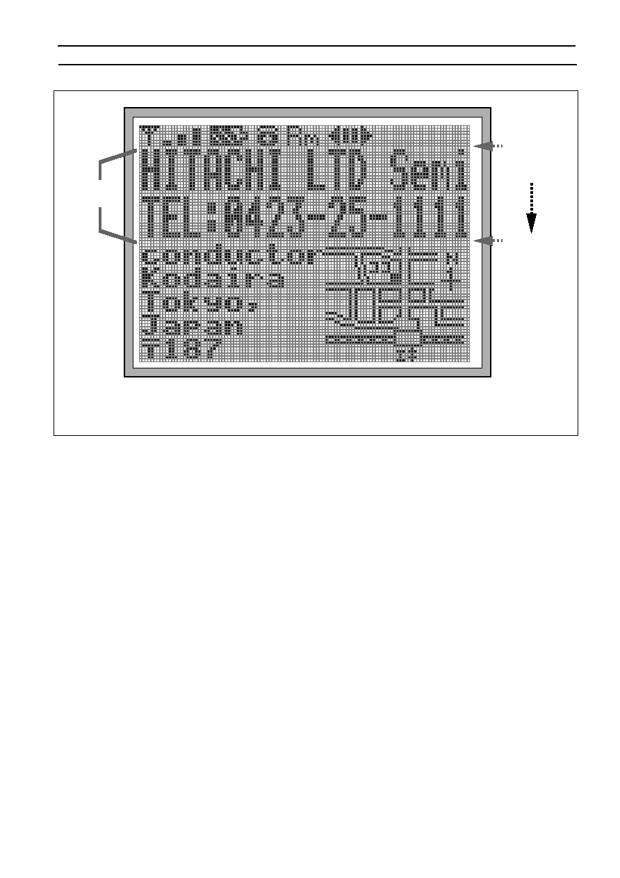
Figure 51 Double-height Display (9th to 40th raster-rows)
HITACHI
76
HD66750/1
• Double-height display on: DHE = 1
• Double-height display start: DS6 to 0 = 0001000
• Double-height display end: DE6 to 0 = 0010111
Start double-
height display
(9th raster-row)
Double-height
display area
End double-
height display
(40th raster-row)

HD66750/1
77
Reversed Display Function
The HD66750/1 can display graphics display sections by black-and-white reversal. Black-and-white
reversal can be easily displayed when the REV bit in the display control register is set to 1.
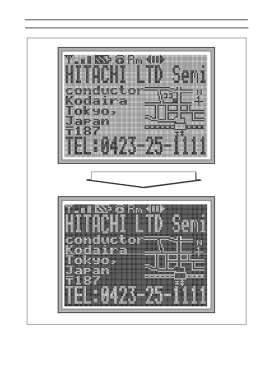
Figure 52 Reversed Display
HITACHI
78
HD66750/1
REV = 1 (Reversed display)

HD66750/1
79
Partial-display-on Function
The HD66750/1 can program the liquid crystal display drive duty ratio setting (NL3-0 bits), the liquid
crystal display drive bias value selection (BS2-0 bits), the boost output level selection (BT1-0 bits), and the
contrast adjustment (CT5-0 bits). For example, when the 128 x 120-dot screen is normally displayed with
a 1/120 duty ratio, the HD66750/1 can selectively drive only the center of the screen or the top of the screen
by combining these register functions and the centering display function (CN bit). This is called partial-
display-on. Lowering the liquid crystal display drive duty ratio reduces the liquid crystal display drive
voltage, thus reducing internal current consumption. This is suitable for a 16 raster-row display (1/16
duty ratio) of a calendar or time in the system-standby state, or the display of only graphics icons
(pictograms) at the top of the screen, which enables continuous display with minimal current consumption.
The non-displayed lines are constantly driven by the unselected level voltage, thus turning off the LCD for
these lines.
In general, lowering the liquid crystal display drive duty ratio decreases the optimum liquid crystal display
drive voltage and liquid crystal display drive bias value. This reduces output multiplying factors in the
booster and greatly controls consumption current.
Table 26 Partial-display-on Function (1/120-duty Normal Drive)
Item
Normal Display
Partial-on Display (Limited to Four-line Display)
LCD screen
128 x 120 dots
128 x 16 dots only on
the center of the screen
128 x 16 dots only at the
top of the screen
LCD drive position
shift
Not necessary
(CN = 0)
Necessary
(CN = 1)
Not necessary
(CN = 0)
LCD drive duty ratio
1/120 (NL3 to 0 = 1110)
1/16 (NL3 to 0 = 0001)
1/16 (NL3 to 0 = 0001)
LCD drive bias
value (optimum)
1/11 (BS2 to 0 = 000)
1/5 (BS2 to 0 = 110)
1/5 (BS2 to 0 = 110)
LCD drive voltage*
13.5 V to 15.5 V
(precisely adjustable
using CT5 to 0)
4 V to 5 V
(precisely adjustable
using CT5 to 0)
4 V to 5 V
(precisely adjustable
using CT5 to 0)
Boosting output
multiplying factor
Six times (BT1 to 0 = 10)
Two times (BT1 to 0 =
00)
Two times (BT1 to 0 =
00)
Frame frequency
(fosc = 70 kHz)
68 Hz
68 Hz
68 Hz
Note:
The LCD drive voltage depends on the LCD materials used. Since the LCD drive voltage is high
when the LCD drive duty ratio is high, a low duty ratio enables low-power consumption.
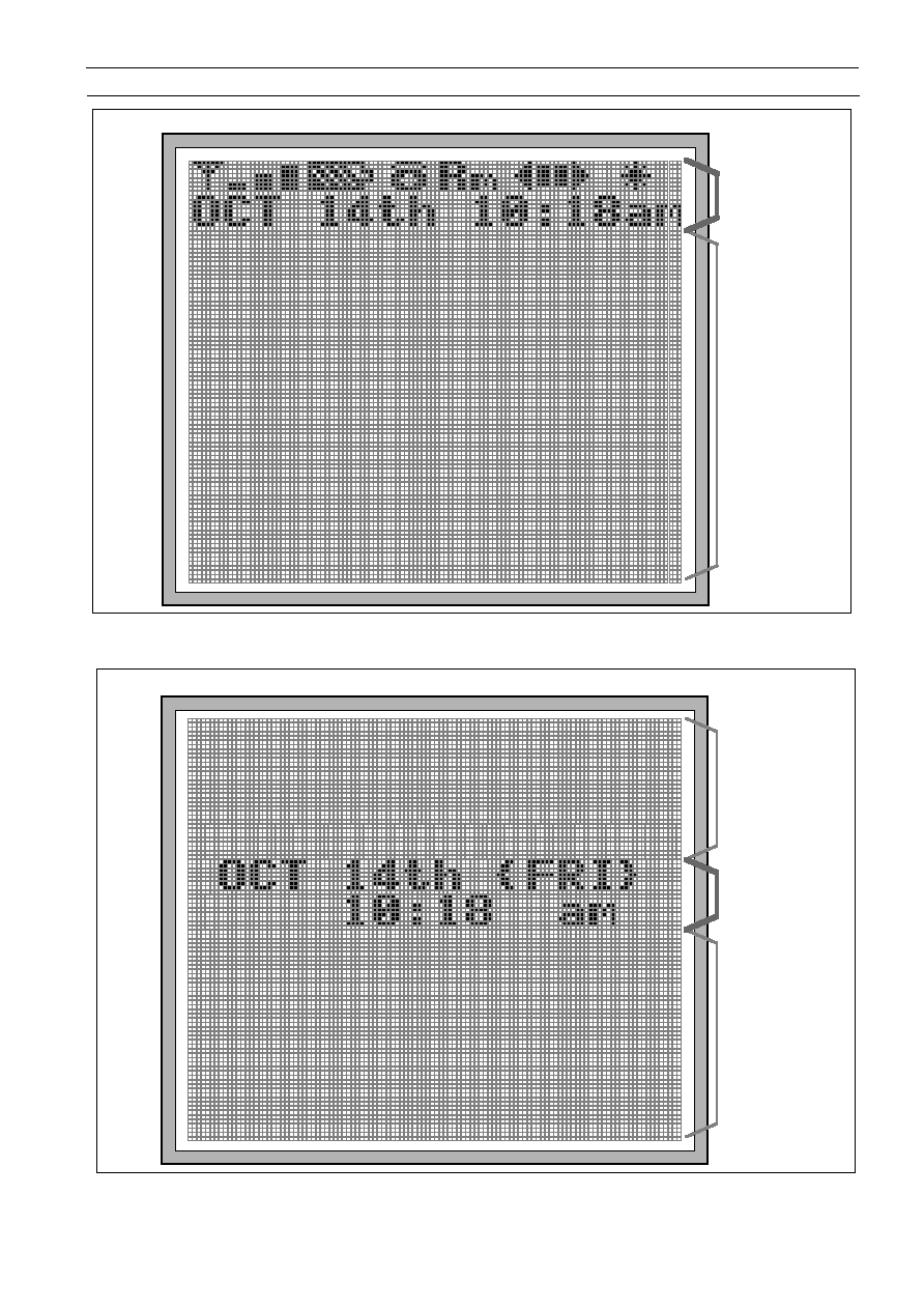
Figure 53 Partial-on Display (Date and Time Indicated) (1)
HITACHI
80
HD66750/1
Figure 54 Partial-on Display (Date and Time Indicated) (2)
i) 1/16-duty Drive at the Top of the Screen
Always applying
non-selection
level
1/16-duty drive
ii) 1/16-duty Drive at the Center of the Screen (Centering Display)
Always
applying non-
selection level
1/16-duty drive
Always
applying non-
selection level
HD66750/1
81
Sleep Mode
Setting the sleep mode bit (SLP) to 1 puts the HD66750/1 in the sleep mode, where the device stops all
internal display operations, thus reducing current consumption. Specifically, LCD operation is completely
halted. Here, all the SEG (SEG1 to SEG128) and COM (COM1 to COM128) pins output the GND level,
resulting in no display. If the AP1-0 bits in the power control register are set to 00 in the sleep mode, the
LCD drive power supply can be turned off, reducing the total current consumption of the LCD module.
Table 27 Comparison of Sleep Mode and Standby Mode
Function
Sleep Mode (SLP = 1)
Standby Mode (STB = 1)
LCD control
Turned off
Turned off
R-C oscillation circuit
Operates normally
Operation stopped
Standby Mode
Setting the standby mode bit (STB) to 1 puts the HD66750/1 in the standby mode, where the device stops
completely, halting all internal operations including the R-C oscillation circuit, thus further reducing
current consumption compared to that in the sleep mode. Specifically, all the SEG (SEG1 to SEG128) and
COM (COM1 to COM128) pins for the multiplexing drive output the GND level, resulting in no display. If
the AP1-0 bits are set to 00 in the standby mode, the LCD drive power supply can be turned off.
During the standby mode, no instructions can be accepted other than the start-oscillation instruction. To
cancel the standby mode, issue the start-oscillation instruction to stabilize R-C oscillation before setting the
STB bit to 0.
Standby mode
Wait at least 10 ms
Turn off the LCD power supply: AP1 to 0 = 00
Set standby mode: STB = 1
Issue the start-oscillation instruction
Cancel standby mode: STB = 0
Turn on the LCD power supply: AP1 to 0 = 01 / 10 / 11
Figure 55 Procedure for Setting and Canceling Standby Mode

HD66750/1
82
Absolute Maximum Ratings
Item
Symbol
Unit
Value
Notes*
Power supply voltage (1)
V
CC
V
–0.3 to +4.6
1, 2
Power supply voltage (2)
V
LCD
– GND
V
–0.3 to +16.5
1, 3
Input voltage
Vt
V
–0.3 to V
CC
+ 0.3
1
Operating temperature
Topr
∞
C
–40 to +85
1, 4
Storage temperature
Tstg
∞
C
–55 to +110
1, 5
Notes: 1. If the LSI is used above these absolute maximum ratings, it may become permanently
damaged. Using the LSI within the following electrical characteristics limits is strongly
recommended for normal operation. If these electrical characteristic conditions are also
exceeded, the LSI will malfunction and cause poor reliability.
2. VCC > GND must be maintained.
3. VLCD > GND must be maintained.
4. For bare die and wafer products, specified up to 85˚C.
5. This temperature specifications apply to the TCP package.

HD66750/1
83
DC Characteristics (V
CC
= 1.8 to 3.6 V, Ta = –40 to +85
∞
C*
1
)
Item
Symbol Min
Typ
Max
Unit Test Condition
Notes
Input high voltage
V
IH
0.7 V
CC
—
V
CC
V
2, 3
Input low voltage
V
IL
–0.3
—
0.15 V
CC
V
V
CC
= 1.8 to 2.4 V
2, 3
–0.3
—
0.15 V
CC
V
V
CC
= 2.4 to 3.6 V
2, 3
Output high voltage (1)
(DB0-15 pins)
V
OH1
0.75 V
CC
—
—
V
I
OH
= –0.1 mA
2
Output low voltage (1)
(DB0-15 pins)
V
OL1
—
—
0.2 V
CC
V
V
CC
= 1.8 to 2.4 V,
I
OL
= 0.1 mA
2
—
—
0.15 V
CC
V
V
CC
= 2.4 to 3.6 V,
I
OL
= 0.1 mA
2
Driver ON resistance
(COM pins)
R
COM
—
3
10
k
±
Id = 0.05 mA,
V
LCD
= 10 V
4
Driver ON resistance
(SEG pins)
R
SEG
—
3
10
k
±
Id = 0.05 mA,
V
LCD
= 10 V
4
I/O leakage current
I
Li
–1
—
1
µ
A
Vin = 0 to V
CC
5
Current consumption
during normal operation
(V
CC
– GND)
I
OP
—
50
(T.B.D.)
90
(T.B.D.)
µ
A
R-C oscillation,
V
CC
= 3 V, Ta = 25
∞
C, f
OSC
= 70 kHz (1/120 duty)
6, 7
Current consumption
during sleep mode
(V
CC
– GND)
I
SL
—
10
—
µ
A
R-C oscillation,
V
CC
= 3 V, Ta = 25
∞
C, f
OSC
= 70 kHz (1/120 duty)
6, 7
Current consumption
during standby mode
(V
CC
– GND)
I
ST
—
0.1
5
µ
A
V
CC
= 3 V, Ta = 25
∞
C
6, 7
LCD drive power supply
current (V
LCD
– GND)
I
LCD
—
25
(T.B.D.)
40
(T.B.D.)
µ
A
V
LCD
= 15 V, 1/11 bias,
Ta = 25
∞
C, f
OSC
= 70 kHz
7
LCD drive voltage
(V
LCD
– GND)
V
LCD
5.0
—
15.5
V
8
Note:
For the numbered notes, refer to the Electrical Characteristics Notes section following these tables.

HD66750/1
84
Booster Characteristics (T. B. D.)
Item
Symbol
Min
Typ
Max
Unit
Test Condition
Notes
Two-times-boost
output voltage
(VLOUT pin)
V
UP2
3.9
4.3
4.4
V
V
CC
= Vci = 2.2 V,
I
O
= 30
µ
A, C = 1
µ
F,
f
OSC
= 70 kHz, Ta = 25
∞
C
11
Five-times-boost
output voltage
(VLOUT pin)
V
UP5
10.5
10.8
11.0
V
V
CC
= Vci = 2.2 V,
I
O
= 30
µ
A, C = 1
µ
F,
f
OSC
= 70 kHz, Ta = 25
∞
C
11
Six-times-boost
output voltage
(VLOUT pin)
V
UP6
12.7
12.9
13.2
V
V
CC
= Vci = 2.2 V,
I
O
= 30
µ
A, C = 1
µ
F,
f
OSC
= 70 kHz, Ta = 25
∞
C
11
Seven-times-
boost output
voltage (VLOUT
pin)
V
UP7
13.9
15.1
15.4
V
V
CC
= Vci = 2.2 V,
I
O
= 30
µ
A, C = 1
µ
F,
f
OSC
= 70 kHz, Ta = 25
∞
C
11
Use range of
boost output
voltages
V
UP2
V
UP5
V
UP6
V
UP7
Vcc
—
15.5
V
For two- to seven-times
boost
11
Note:
For the numbered notes, refer to the Electrical Characteristics Notes section following these tables.

HD66750/1
85
AC Characteristics (V
CC
= 1.8 to 3.6 V, Ta = –40 to +85
∞
C*
1
)
Clock Characteristics (V
CC
= 1.8 to 3.6 V)
Item
Symbol
Min
Typ
Max
Unit
Test Condition
Notes
External clock
frequency
fcp
50
75
150
kHz
9
External clock duty
ratio
Duty
45
50
55
%
9
External clock rise
time
trcp
—
—
0.2
µ
s
9
External clock fall
time
tfcp
—
—
0.2
µ
s
9
R-C oscillation clock
f
OSC
59
74
89
kHz
Rf = 390 k
,
V
CC
= 3 V
10
Note:
For the numbered notes, refer to the Electrical Characteristics Notes section following these tables.
68-system Bus Interface Timing Characteristics
(Vcc = 1.8 to 2.4 V)
Item
Symbol Min
Typ
Max
Unit
Test Condition
Enable cycle time
Write t
CYCE
600
—
—
ns
Figure 62
Read t
CYCE
800
—
—
Enable high-level pulse width
Write PW
EH
120
—
—
ns
Figure 62
Read PW
EH
350
—
—
Enable low-level pulse width
Write PW
EL
300
—
—
ns
Figure 62
Read PW
EL
300
—
—
Enable rise/fall time
t
Er
, t
Ef
—
—
25
ns
Figure 62
Setup time (RS, R/W to E, CS*)
t
ASE
50
—
—
ns
Figure 62
Address hold time
t
AHE
20
—
—
ns
Figure 62
Write data setup time
t
DSWE
60
—
—
ns
Figure 62
Write data hold time
t
HE
20
—
—
ns
Figure 62
Read data delay time
t
DDRE
—
—
300
ns
Figure 62
Read data hold time
t
DHRE
5
—
—
ns
Figure 62

HD66750/1
86
(Vcc = 2.4 to 3.6 V)
Item
Symbol Min
Typ
Max
Unit
Test Condition
Enable cycle time
Write t
CYCE
380
—
—
ns
Figure 62
Read t
CYCE
500
—
—
Enable high-level pulse width
Write PW
EH
70
—
—
ns
Figure 62
Read PW
EH
250
—
—
Enable low-level pulse width
Write PW
EL
150
—
—
ns
Figure 62
Read PW
EL
150
—
—
Enable rise/fall time
t
Er
, t
Ef
—
—
25
ns
Figure 62
Setup time (RS, R/W to E, CS*)
t
ASE
50
—
—
ns
Figure 62
Address hold time
t
AHE
20
—
—
ns
Figure 62
Write data setup time
t
DSWE
60
—
—
ns
Figure 62
Write data hold time
t
HE
20
—
—
ns
Figure 62
Read data delay time
t
DDRE
—
—
200
ns
Figure 62
Read data hold time
t
DHRE
5
—
—
ns
Figure 62

HD66750/1
87
80-system Bus Interface Timing Characteristics
(Vcc = 1.8 to 2.4 V)
Item
Symbol Min
Typ
Max
Unit
Test Condition
Bus cycle time
Write t
CYCW
600
—
—
ns
Figure 63
Read t
CYCR
800
—
—
ns
Figure 63
Write low-level pulse width
PW
LW
120
—
—
ns
Figure 63
Read low-level pulse width
PW
LR
350
—
—
ns
Figure 63
Write high-level pulse width
PW
HW
300
—
—
ns
Figure 63
Read high-level pulse width
PW
HR
300
—
—
ns
Figure 63
Write/Read rise/fall time
t
WRr
,
WRf
—
—
25
ns
Figure 63
Setup time (RS to CS*, WR*, RD*)
t
AS
50
—
—
ns
Figure 63
Address hold time
t
AH
20
—
—
ns
Figure 63
Write data setup time
t
DSW
60
—
—
ns
Figure 63
Write data hold time
t
H
20
—
—
ns
Figure 63
Read data delay time
t
DDR
—
—
300
ns
Figure 63
Read data hold time
t
DHR
5
—
—
ns
Figure 63
(Vcc = 2.4 to 3.6 V)
Item
Symbol Min
Typ
Max
Unit
Test Condition
Bus cycle time
Write t
CYCW
380
—
—
ns
Figure 63
Read t
CYCR
500
—
—
ns
Figure 63
Write low-level pulse width
PW
LW
70
—
—
ns
Figure 63
Read low-level pulse width
PW
LR
250
—
—
ns
Figure 63
Write high-level pulse width
PW
HW
150
—
—
ns
Figure 63
Read high-level pulse width
PW
HR
150
—
—
ns
Figure 63
Write/Read rise/fall time
t
WRr, WRf
—
—
25
ns
Figure 63
Setup time (RS to CS*, WR*, RD*)
t
AS
50
—
—
ns
Figure 63
Address hold time
t
AH
20
—
—
ns
Figure 63
Write data setup time
t
DSW
60
—
—
ns
Figure 63
Write data hold time
t
H
20
—
—
ns
Figure 63
Read data delay time
t
DDR
—
—
200
ns
Figure 63
Read data hold time
t
DHR
5
—
—
ns
Figure 63
Reset Timing Characteristics (V
CC
= 1.8 to 3.6 V)
Item
Symbol
Min
Typ
Max
Unit
Test Condition
Reset low-level width
t
RES
1
—
—
ms
Figure 64
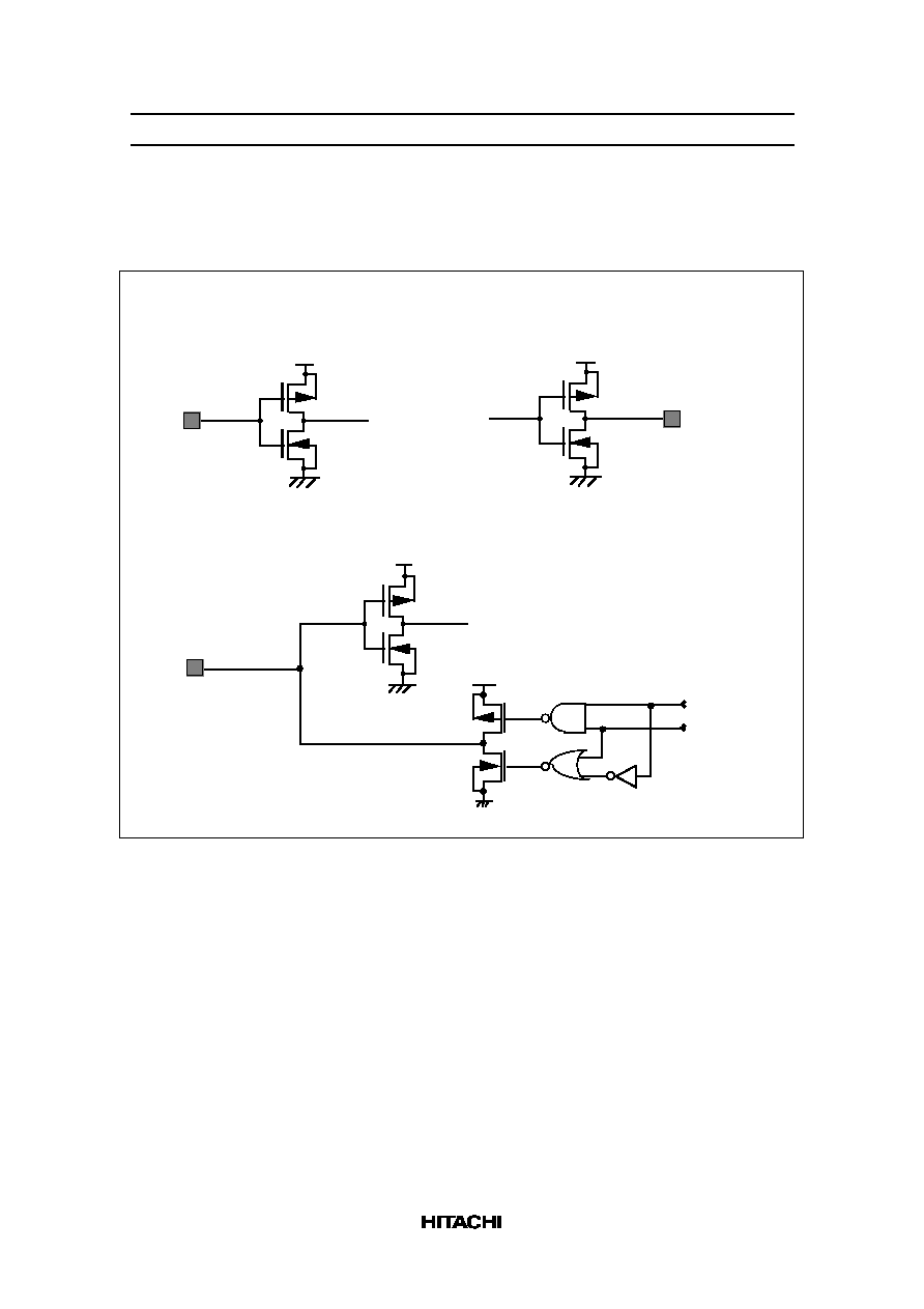
HD66750/1
88
Electrical Characteristics Notes
1. For bare die products, specified up to 85˚C.
2. The following three circuits are I/O pin configurations (figure 56).
Pins: RESET*, CS*, E/WR, RW/RD, RS, OSC1,
OPOFF, IM1/0, TEST
Pin: OSC2
PMOS
NMOS
Vcc
GND
Pins: DB15 to DB0
PMOS
NMOS
Vcc
GND
NMOS
PMOS
Vcc
Vcc
PMOS
NMOS
(Tri-state output circuit)
Output data
Output enable
GND
PMOS
(Input circuit)
Figure 56 I/O Pin Configuration
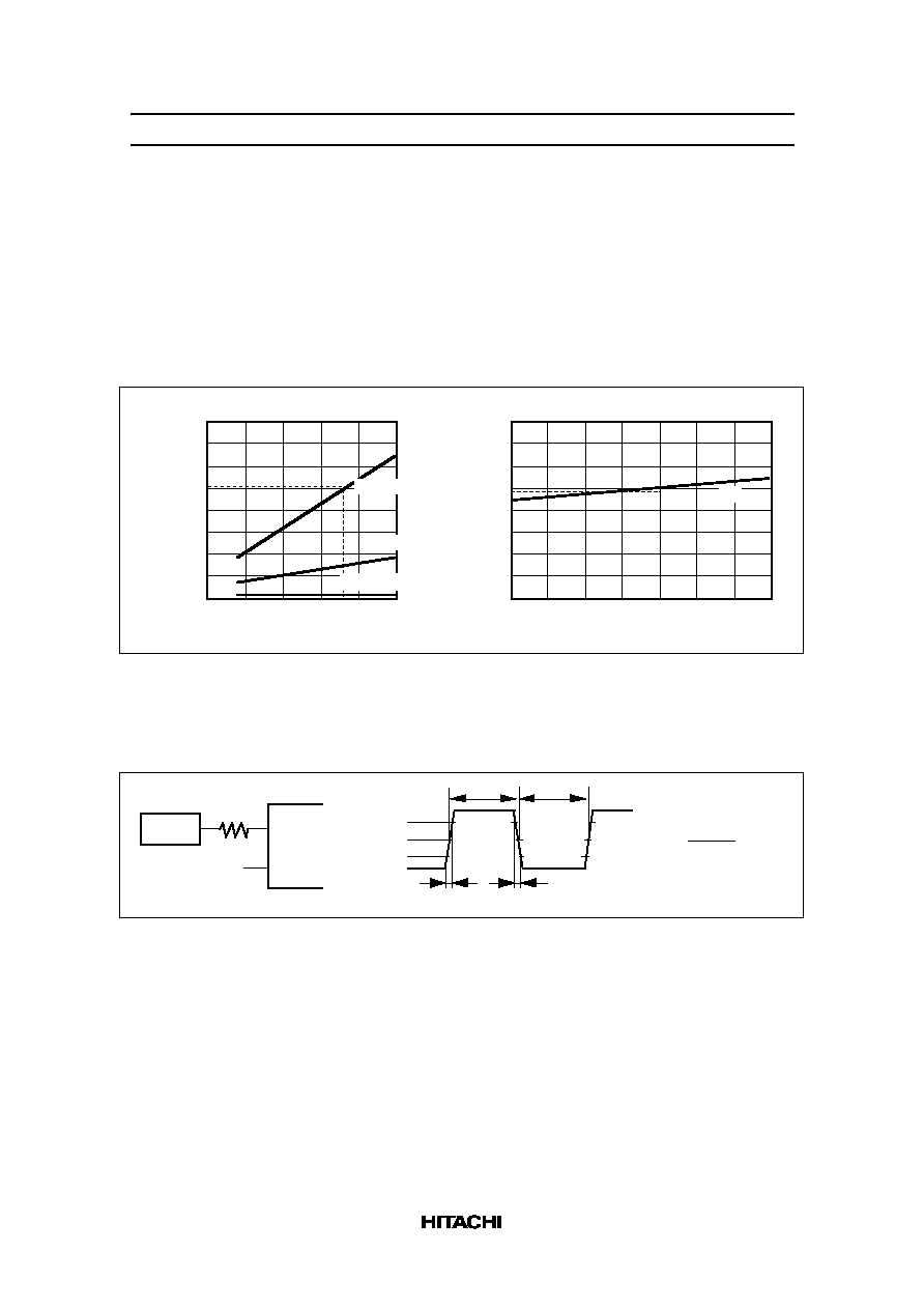
HD66750/1
89
3. The TEST pin must be grounded and the IM1/0 and OPOFF pins must be grounded or connected to
Vcc.
4. Applies to the resistor value (RCOM) between power supply pins V1OUT, V2OUT, V5OUT, GND and
common signal pins, and resistor value (RSEG) between power supply pins V1OUT, V3OUT, V4OUT,
GND and segment signal pins.
5. This excludes the current flowing through output drive MOSs.
6. This excludes the current flowing through the input/output units. The input level must be fixed high or
low because through current increases if the CMOS input is left floating.
7. The following shows the relationship between the operation frequency (fosc) and current consumption
(Icc) (figure 57).
R-C oscillation frequencies: fosc (kHz)
60
40
20
0
Iop (
µ
A)
Vcc = 3V
0
Display on (typ.)
Sleep (typ.)
30
20
10
0
ILCD (
µ
A)
Vcc = 3 V, fosc = 70 kHz
11.0
LCD drive voltage: VLCD (V)
13.0
15.0
17.0
Standby (typ.)
40
20
60
80
100
typ.
<T.B.D>
<T.B.D>
Figure 57 Relationship between the Operation Frequency and Current Consumption
8. Each COM and SEG output voltage is within
±
0.15 V of the LCD voltage (Vcc, V1, V2, V3, V4, V5)
when there is no load.
9. Applies to the external clock input (figure 58).
Oscillator
OSC1
Open
OSC2
t rcp
tfcp
Th
Tl
0.7Vcc
0.5Vcc
0.3Vcc
Duty =
Th + Tl
Th
x 100%
2 k
Figure 58 External Clock Supply
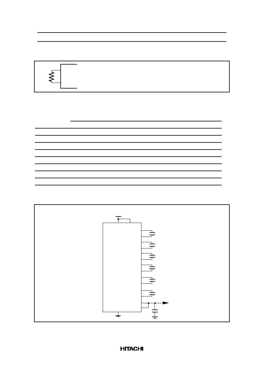
HD66750/1
90
10. Applies to the internal oscillator operations using external oscillation resistor Rf (figure 59 and table
28).
OSC1
OSC2
Rf
Since the oscillation frequency varies depending on the OSC1 and OSC2 pin
capacitance, the wiring length to these pins should be minimized.
Figure 59 Internal Oscillation
Table 28 External Resistance Value and R-C Oscillation Frequency (Referential Data)
External
R-C Oscillation Frequency: fosc
Resistance (Rf)
Vcc = 1.8 V
Vcc = 2.2 V
Vcc = 3.0 V
Vcc = 4.0 V
200 k
86 kHz
111 kHz
130 kHz
140 kHz
270 k
70 kHz
86 kHz
100 kHz
108 kHz
300 k
64 kHz
79 kHz
92 kHz
98 kHz
330 k
60 kHz
74 kHz
86 kHz
91 kHz
360 k
57 kHz
69 kHz
79 kHz
84 kHz
390 k
54 kHz
64 kHz
74 kHz
78 kHz
430 k
49 kHz
59 kHz
67 kHz
71 kHz
470 k
46 kHz
54 kHz
61 kHz
65 kHz
11. Booster characteristics test circuits are shown in figure 60.
(Five to seven times b oosting
V cc
1
µ
F
V ci
C1+
C1-
+
GND
V LOUT
V
LCD
1
µ
F
+
1
µ
F
C2+
C2-
1
µ
F
C3+
C3-
C4+
C4-
+
+
C5+
C5-
C6+
C6-
1
µ
F
+
1
µ
F
+
1
µ
F
+
Figure 60 Booster
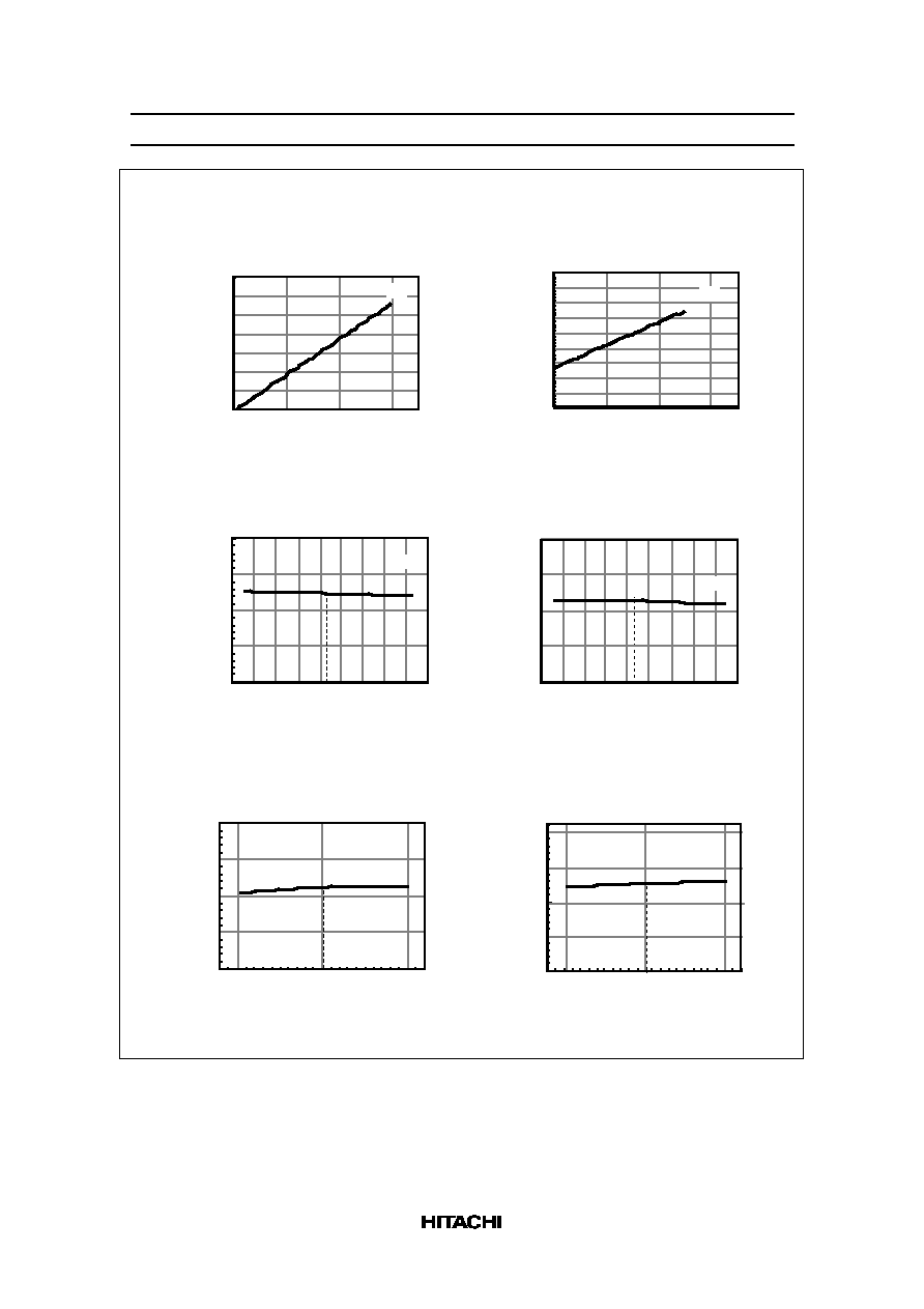
HD66750/1
91
VUP6 = VLCD - GND, VUP7 = VLCD - GND
(i) Relation between the obtained voltage and input voltage
Vci = Vcc = 2.4 V, fosc = 70 kHz, Io = 30
µ
A,
DC1 to 0= 00
(ii) Relation between the obtained voltage and temperature
Vci = Vcc = 2.4 V, fosc = 70 kHz, Io = 30
µ
A,
DC1 to 0 = 00
Referential data
3.0
2.5
2.0
1.5
9.0
12.0
15.0
18.0
Vci (V)
VUP6 (V)
typ.
Vci = Vcc, fosc = 70 kHz, Ta = 25
∞
C, DC1 to 0= 00
3.0
2.5
2.0
1.5
8.0
13.0
typ.
Vci = Vcc, fosc = 70 kHz, Ta = 25
∞
C, DC1 to 0 = 00
VUP7 (V)
Vci (V)
Six-times boosting
Seven-times boosting
18.0
Six-times boosting
Seven-times boosting
Ta (
∞
C)
VUP6 (V)
100
60
20
0
-20
-60
11.0
13.0
15.0
17.0
typ.
Ta (
∞
C)
VUP7 (V)
100
60
20
0
-20
-60
14.0
16.0
18.0
typ.
<T.B.D>
<T.B.D>
<T.B.D>
<T.B.D>
(iii) Relation between the obtained voltage and capacity
Vci = Vcc = 2.4 V, fosc = 70 kHz, Io = 30
µ
A,
DC1 to 0 = 00
Vci = Vcc = 2.4 V, fosc = 70 kHz, Io = 30
µ
A,
DC1 to 0 = 00
1.5
1.0
0.5
14.0
15.0
16.0
17.0
typ.
C (
µ
F)
VUP7 (V)
Six-times boosting
Seven-times boosting
C (
µ
F)
VUP6 (V)
1.5
1.0
0.5
11.0
13.0
14.0
15.0
16.0
typ.
18.0
<T.B.D>
<T.B.D>
Figure 60 Booster (cont)
HD66750/1
92
(iv) Relation between the obtained voltage and current
Vci = Vcc = 2.4 V, fosc = 70 kHz, Ta = 25
∞
C,
DC1 to 0 = 00
Vci = Vcc = 2.4 V, fosc = 70 kHz, Ta = 25
∞
C,
DC1 to 0 = 00
Io (
µ
A)
VUP6 (V)
200
150
100
50
0
13.0
13.5
14.0
14.5
15.0
Io (
µ
A)
VUP7 (V)
200
150
100
50
0
15.5
16.0
16.5
17.0
17.5
Six-times boosting
Seven-times boosting
<T.B.D>
<T.B.D>
Figure 60 Booster (cont)
Load Circuits
AC Characteristics Test Load Circuits
Data bus: DB15 to DB0
Test Point
50 pF
Figure 61 Load Circuit

HD66750/1
93
Timing Characteristics
68-system Bus Operation
RS
R/W
CS*
E
DB0
to DB15
DB0
to DB15
V
IH
V
IL
t
ASE
t
AHE
PW
EH
t
Ef
t
Er
t
D SWE
t
HE
Write data
t
CYCE
t
D DRE
t
DHR E
V
OH1
V
OL1
V
OH1
V
OL1
Read data
V
IH
V
IL
V
IL
V
IL
V
IH
V
IH
V
IL
V
IH
V
IL
V
IH
V
IL
PW
EL
Note 1: PW
EH
is specified in the overlapped period when CS* is low and E is high.
V
IL
V
IL
*1
Figure 62 68-system Bus Timing
HD66750/1
94
80-system Bus Operation
RS
CS*
WR*
RD*
V
IH
V
IL
t
AS
t
AH
PW
LW,
PW
LR
t
WRf
t
WRr
t
DSW
t
HWR
Write data
t
CYC W,
t
CYCR
t
DDR
t
D HR
V
OH1
V
OL1
V
OH1
V
OL1
Read data
V
IH
V
IL
V
IH
V
IL
V
IH
V
IL
V
IH
V
IL
V
IH
V
IL
V
IH
V
IL
V
IH
PW
HW
PW
HR
Note 1: PW
LW
and PW
L R
are s pecified in the overlapped period when CS* is low and W R* or RD* is low.
DB0
to DB15
DB0
to DB15
*1
Figure 63 80-system Bus Timing
Reset Operation
RESET*
V
IL
V
IL
t
RES
Figure 64 Reset Timing
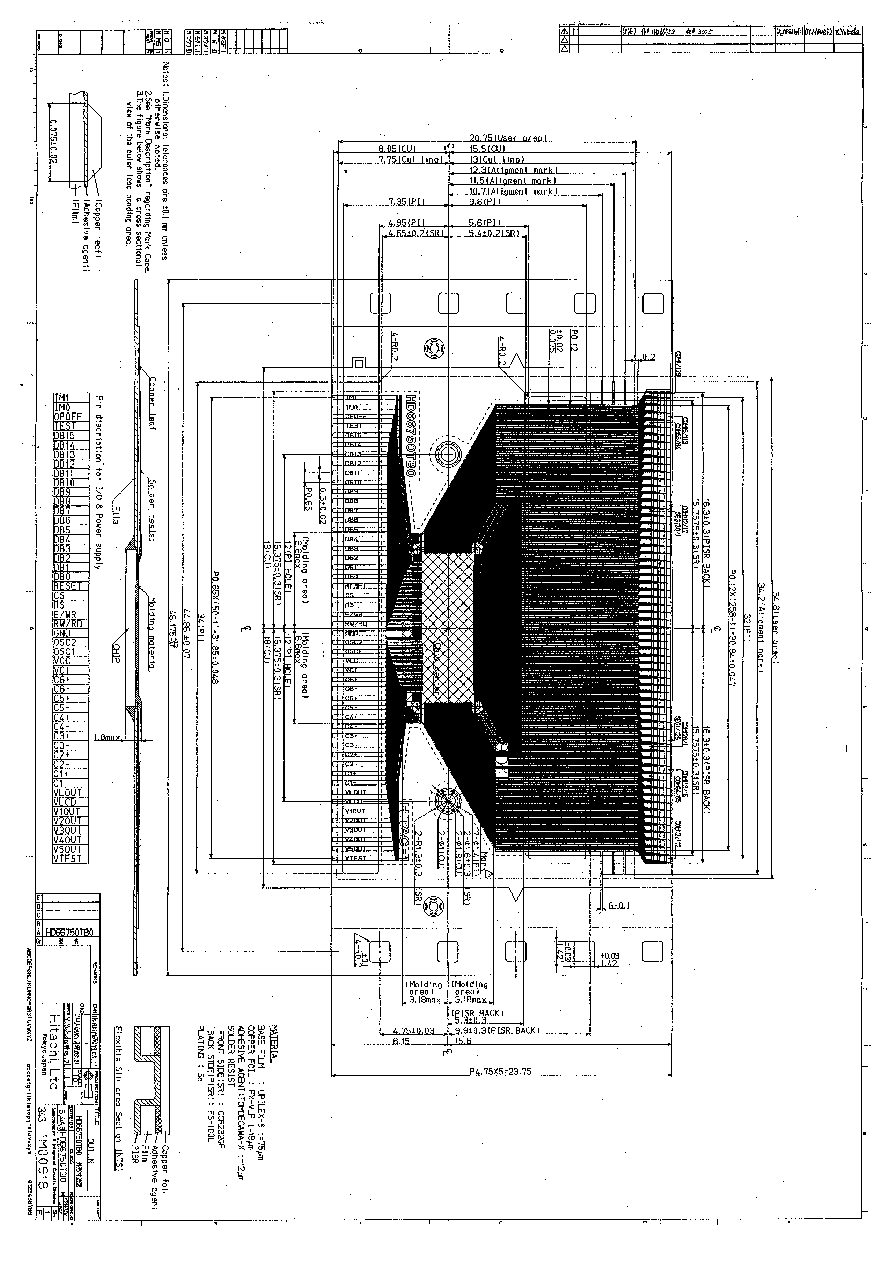

When using this document, keep the following in mind:
1. This document may, wholly or partially, be subject to change without notice.
2. All right reserved: No one is permitted to reproduce or duplicated, in any form, the whole or part of this
document without Hitachi's permission.
3. Hitachi will not be held responsible for any damage to the user that may result from accidents or any other
reasons during operation of the user's unit according to this document.
4. Circuitry and other examples described herein are meant merely to indicate the characteristics and
performance of Hitachi's semiconductor products. Hitachi assumes no responsibility for any intellectual
property claims or other problems that may result from applications based on the examples described
herein.
5. No license is granted by implication or otherwise under any patents or other rights of any third party of
Hitachi, Ltd.
6. MEDICAL APPLICATIONS: Hitachi's products are not authorized for use in MEDICAL
APPLICATIONS without the written consent of the appropriate officer of Hitachi's sales company. Such
use includes, but is not limited to use in life support systems. Buyers of Hitachi's products are requested to
notify the relevant Hitachi sales offices when planning to use the products in MEDICAL
APPLICATIONS.