 | –≠–ª–µ–∫—Ç—Ä–æ–Ω–Ω—ã–π –∫–æ–º–ø–æ–Ω–µ–Ω—Ç: HD293486 | –°–∫–∞—á–∞—Ç—å:  PDF PDF  ZIP ZIP |
HD293486
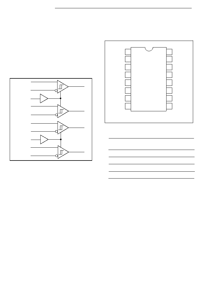
Quadruple Dfferential Line Receivers With 3 State Outputs
The HD293486 features quadruple Differential
line receivers designed to meet the specs of EIA
RS≠422A and RS≠423A. This device operates
from a single 5 V power supply. When the
enable input is low the associated outputs are in a
high impedance state.
Function Table
H
L
X
?
Z
Differential Input
A ≠ B
V
ID
0.2 V
≠0.2 V
<
V
ID
<
0.2 V
V
ID
≠0.2 V
X
Output Enable
H
H
H
L
Output
Y
H
?
L
Z
:
:
:
:
:
High level
Low level
Irrelevant
Indeterminate
High Impedance
1Y
2Y
3Y
4Y
Pin Arrangement
Enable
1
2
3
4
5
6
7
8
9
10
11
12
13
14
15
16
1,2 Output
Enable
1B
1A
1Y
2Y
2A
2B
GND
3,4 Output
3B
3A
3Y
4Y
4A
4B
Vcc
(Top View)
Logic Diagram
1A
1B
3A
3B
1,2 Output
Enable
2A
2B
3,4 Output
Enable
4A
4B

2
Absolute Maximum Ratings
Item
Supply Voltage
A , B Input Voltage
Differential Input Voltage
Enable Input Voltage
Output Current
Power Dissipation
Symbol
V
CC
V
IN
V
ID
V
IE
I
OL
P
T
*3
Ratings
7.0
±
15.0
±
25.0
7.0
50
1000
Unit
V
V
V
V
mA
mW
Operating Temperature
Storage Temperature
Topr
Tstg
0 to +70
∞
C
∞
C
to +150
≠65
*2
HD293486
2. All voltage values except for differential input voltage are with respect to ground terminal.
3. Differential input voltage is measured at the noninverting input with respect to the
corresponding inverting input.
4. The absolute maximum ratings are values which must not individually be exceeded, and
furthemore, no two of which may be realized at the same time.
Recommended Operating Conditions
Item
Supply Voltage
In Phase Input Voltage
Differential Input Voltage
Output Current
Operating Temperature
Symbol
V
CC
V
IC
V
ID
I
OH
I
OL
Min
4.75
0
Typ
5.00
Max
5.25
±
7
±
6
8.0
70
Unit
V
V
V
mA
mA
∞
C
≠0.4
Topr
Notes: 1. The above data were taken by the
V
EB
method mounting on a glass epoxy board
(40
◊
40
◊
1.6 mm) of 10 % wiring density.
DP
FP
*1
785
HD293486
3
V
ID
2 V
V
OH
V
OL
500
500
HD293486
Electrical Characteristics (Ta = 0 to +70
∞
C)
Item
Symbol
Min
Typ
Max
Unit
Conditions
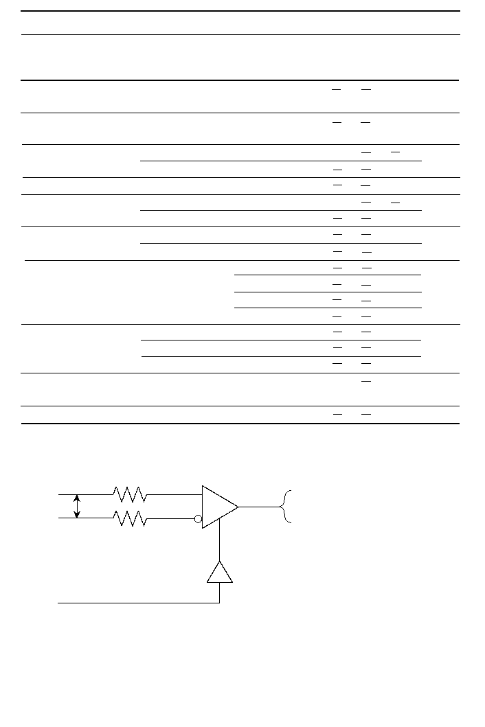
Differential Input
High Threshold Voltage
Output Voltage
Enable Input Current
mA
V
TH
V
IH
V
IL
I
OZ
V
OH
I
IB
I
CC
Vo = 2.7 V, Io = ≠0.4 mA
Differential Input
Low Threshold Voltage
V
TL
Vo = 0.5 V, Io = 8 mA
Enable Input Voltage
Input Clamp Voltage
V
IK
I
I
= ≠10 mA
V
ID
= 0.4 V, I
O
= ≠0.4 mA
V
V
V
V
V
V
OL
V
ID
= ≠0.4 V, I
O
= 8 mA
2.0
2.7
0.2
≠0.2
0.8
≠1.5
0.5
Off State Output
Current
I
OZ
V
IE
= 0.8 V, V
ID
= ≠3 V, V
O
= 2.7 V
40
40
V
IE
= 0.8 V, V
ID
= 3V, V
O
= 0.5V
µ
A
Differential Input
Bias Current
Vcc = 0 V
or 5.25 V
Other
Input = 0 V
V
I
= ≠10 V
V
I
= ≠3 V
V
I
= 3 V
V
I
= 10 V
I
IH
V
I
= 5.25 V
V
I
= 2.7 V
V
I
= 0.5 V
I
IH
I
IL
µ
A
Short Circuit Output
Current
I
OS
V
ID
= 3 V, V
O
= 0 V
≠15
≠3.25
≠1.5
1.5
3.25
100
20
≠100
≠100
V
IE
= 0 V
85
mA
mA
Supply Current
Note: 1. Not more than one output should be shorted at a time.
*1
*1
*2
*1
HD293486
4
Switching Characteristics (V
CC
= 5 V, Ta = 25
∞
C)
Item
Symbol
Min
Typ
Max
Unit
Propagation Delay Time
Output Enable Time
Conditions
Output Disable Time
t
PLH
t
PHL
t
HZ
t
ZL
t
ZH
t
LZ
C
L
= 15 pF
28
27
26
27
13
20
35
30
35
35
30
30
ns
ns
ns
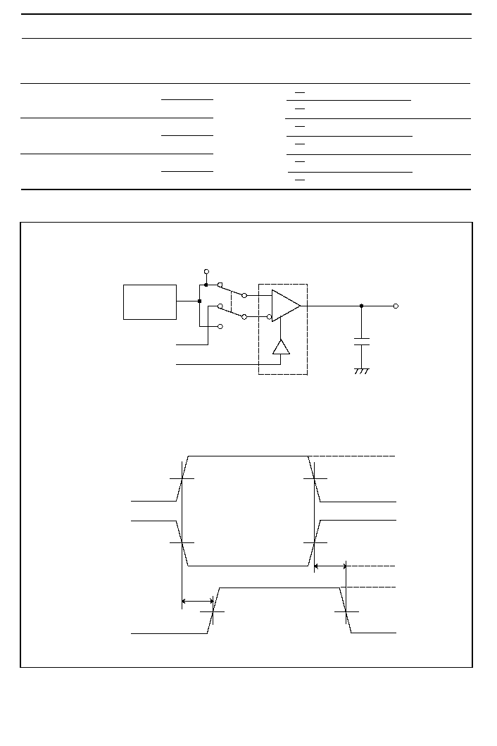
1. t
PLH
, t
PHL
Test circuit
Pulse
Generator
1.5 V
2 V
Input
Output
C
L
= 15 pF
Notes : 1. The pulse generator has following characteristics:
PRR = 1 MH
Z
, 50 % duty cycle, tr
6ns, tf
6ns, Zout = 50
2. C
L
includes probe and jig capacitance.
Waveforms
1.5 V
1.5 V
1.5 V
1.5 V
3 V
0 V
3 V
0 V
V
OH
V
OL
Input A
Input B
1.3 V
1.3 V
t
PLH
Output
t
PHL
Switching Time Test Method
HD293486
HD293486
5
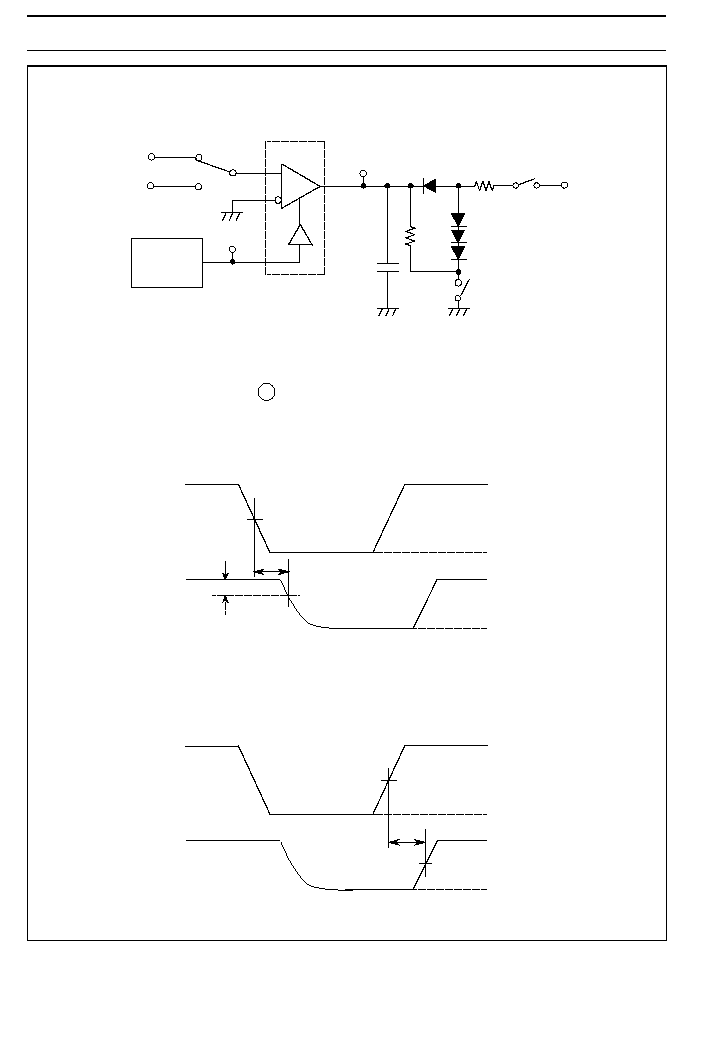
2. t
HZ
, t
ZH
, t
LZ
, t
ZL
Test circuit
(2) t
ZH
Waveforms
(1) t
HZ
1.3 V
Input
Output
V
OH
SW1 to 1.5 V
SW2 CLOSE
SW3 CLOSE
t
HZ
0.5 V
3 V
0 V
1.5 V
≠1.5 V
1.5 V
SW 1
Input
Output
C
L
=
15 pF
5 K
2 K
SW2
5 V
SW3
Pulse
Generator
Notes: 1. The pulse generator has following characteristics:
PRR = 1 MH
Z
, 50 % duty cycle, t
r
6 ns, t
f
6 ns, Zout = 50
2. C
L
includes probe and jig capacitance.
3. All diodes are 1S2074 H
Input
Output
V
OH
SW1 to 1.5 V
SW2 OPEN
SW3 CLOSE
3 V
0 V
1.5 V
t
HZ
1.3 V
1.5 V
HD293486
HD293486