 | –≠–ª–µ–∫—Ç—Ä–æ–Ω–Ω—ã–π –∫–æ–º–ø–æ–Ω–µ–Ω—Ç: HD404336S | –°–∫–∞—á–∞—Ç—å:  PDF PDF  ZIP ZIP |

HD404339 Series
Rev. 7.0
Sept. 1999
Description
The HD404339 Series is 4-bit HMCS400-Series microcomputer with large-capacity memory designed to
increase program productivity. Each microcomputer has an A/D converter, input capture timer, and a 32-
kHz oscillator circuit for clock use all built in. They also come with high-voltage I/O pins that can directly
drive a fluorescent display.
The HD404339 Series includes six chips: the HD404339 with 16-kword ROM; the HD4043312 with 12-
kword ROM; the HD404338 with 8-kword ROM; the HD404336 with 6-kword ROM; the HD404334 with
4-kword ROM; the HD4074339 with 16-kword PROM.
The HD4074339 is a PROM version ZTAT
TM
microcomputer. Programs can be written to the PROM by a
PROM writer, which can dramatically shorten system development periods and smooth the process from
debugging to mass production. (The PROM program specifications are the same as for the 27256.)
ZTAT
TM
: Zero Turn Around Time ZTAT is a trademark of Hitachi Ltd.
Features
∑
54 I/O pins
One input-only pin
53 input/output pins: 30 pins are high-voltage pins (40 V, max.)
∑
On-chip A/D converter (8-bit
◊
12-channel)
∑
Three timers
One event counter input
One timer output
One input capture timer
∑
8-bit clock-synchronous serial interface (1 channel)
∑
Alarm output
∑
Built-in oscillators
Ceramic or crystal oscillator
External clock drive is also possible
Subclock: 32.768-kHz crystal oscillator

HD404339 Series
2
∑
Seven interrupt sources
Two by external sources
Three by timers
One each by the A/D converter and serial interface
∑
Four low-power dissipation modes
Standby mode
Stop mode
Watch mode
Subactive mode
∑
Instruction cycle time: 1
µ
s (f
OSC
= 4 MHz, 1/4 division ratio)
1/4, 1/8, 1/16, 1/32 system clock division ratio can be selected
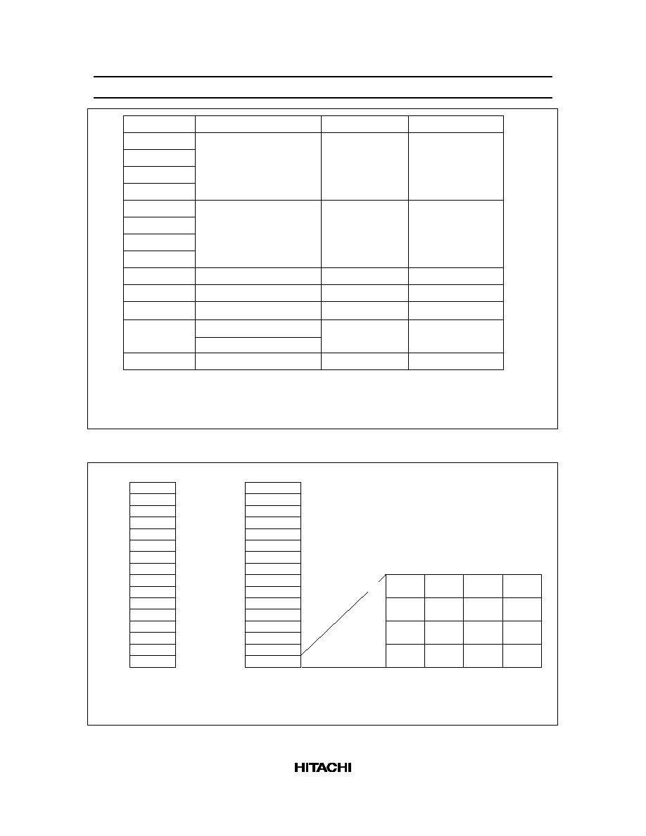
Ordering Information
Type
Product Name
Model Name
ROM (words)
RAM (digit)
Package
Mask ROM
HD404334
HD404334S
4,096
512
DP-64S
HD404334FS
FP-64B
HD404336
HD404336S
6,144
DP-64S
HD404336FS
FP-64B
HD404338
HD404338S
8,912
DP-64S
HD404338FS
FP-64B
HD4043312
HD4043312S
12,288
DP-64S
HD4043312FS
FP-64B
HD404339
HD404339S
16,384
DP-64S
HD404339FS
FP-64B
ZTAT
TM
HD4074339
HD4074339S
16,384
DP64S
HD4074339FS
FP-64B
Recommended PROM Programmers and Socket Adapters
PROM Programmer
Socket Adapter
Manufacture
Model Name
Package
Manufacture
Model Name
DATA I/O corp
121 B
DP-64S
Hitachi
HS4339ESS01H
FP-64B
HS4339ESF01H
AVAL corp
PKW-1000
DP-64S
Hitachi
HS4339ESS01H
FP-64B
HS4339ESF01H
HD404339 Series
3
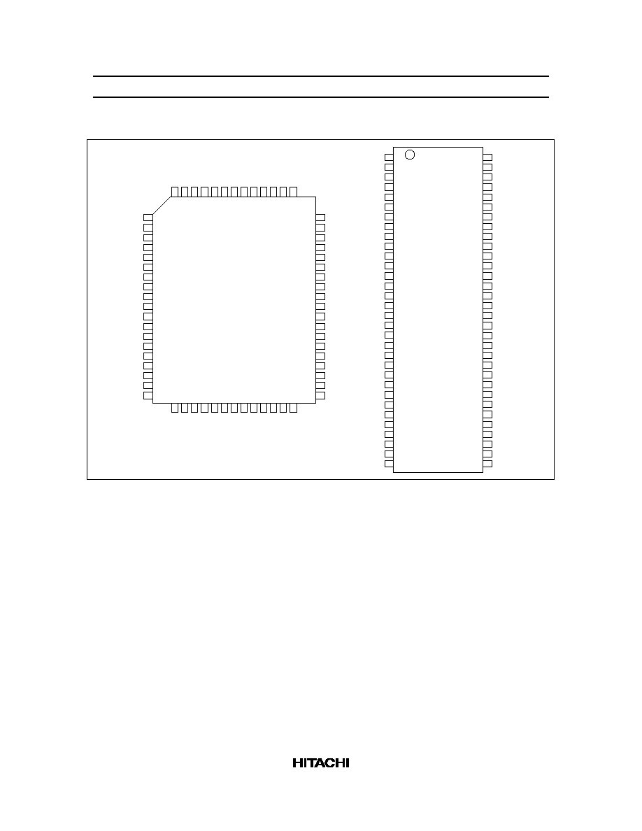
Pin Arrangement
1
2
3
4
5
6
7
8
9
10
11
12
13
14
15
16
17
18
19
51
50
49
48
47
46
45
44
43
42
41
40
39
38
37
36
35
34
33
20
21
22
23
24
25
26
27
28
29
30
31
32
64
63
62
61
60
59
58
57
56
55
54
53
52
FP-64B
R7
2
R0
0
/
SCK
R0
1
/SI
R0
2
/SO
R0
3
/TOC
TEST
RESET
OSC
1
OSC
2
GND
X1
X2
AV
SS
R3
0
/AN
0
R3
1
/AN
1
R3
2
/AN
2
R3
3
/AN
3
R4
0
/AN
4
R4
1
/AN
5
R7
1
R7
0
R6
3
R6
2
R6
1
R6
0
RA
1
/V
disp
R2
3
R2
2
R2
1
R2
0
R1
3
R1
2
R4
2
/AN
6
R4
3
/AN
7
R5
0
/AN
8
R5
1
/AN
9
R5
2
/AN
10
R5
3
/AN
11
AV
CC
V
CC
D
0
/
INT
0
D
1
/
INT
1
D
2
/EVNB
D
3
/BUZZ
D
4
/
STOPC
R1
1
R1
0
R9
3
R9
2
R9
1
R9
0
R8
3
R8
2
R8
1
R8
0
D
13
D
12
D
11
D
10
D
9
D
8
D
7
D
6
D
5
R6
0
R6
1
R6
2
R6
3
R7
0
R7
1
R7
2
R0
0
/
SCK
R0
1
/SI
R0
2
/SO
R0
3
/TOC
TEST
RESET
OSC
1
OSC
2
GND
X1
X2
AV
SS
R3
0
/AN
0
R3
1
/AN
1
R3
2
/AN
2
R3
3
/AN
3
R4
0
/AN
4
R4
1
/AN
5
R4
2
/AN
6
R4
3
/AN
7
R5
0
/AN
8
R5
1
/AN
9
R5
2
/AN
10
R5
3
/AN
11
AV
CC
R8
3
R8
2
R8
1
R8
0
D
13
D
12
D
11
D
10
D
9
D
8
D
7
D
6
D
5
D
4
/
STOPC
D
3
/BUZZ
D
2
/EVNB
D
1
/
INT
1
D
0
/
INT
0
V
CC
RA
1
/V
disp
R2
3
R2
2
R2
1
R2
0
R1
3
R1
2
R1
1
R1
0
R9
3
R9
2
R9
1
R9
0
DP-64S
1
2
3
4
5
6
7
8
9
10
11
12
13
14
15
16
17
18
19
20
21
22
23
24
25
26
27
28
29
30
31
32
51
50
49
48
47
46
45
44
43
42
41
40
39
38
37
36
35
34
33
64
63
62
61
60
59
58
57
56
55
54
53
52

HD404339 Series
4
Pin Description
Pin Number
Item
Symbol
DP-64S
FP-64B
I/O
Function
Power supply
V
CC
33
27
Applies power voltage
GND
16
10
Connected to ground
V
disp
(shared
with RA
1
)
64
58
Used as a high-voltage output power supply pin
when selected by the mask option
Test
TEST
12
6
I
Cannot be used in user applications. Connect
this pin to GND.
Reset
RESET
13
7
I
Resets the MCU
Oscillator
OSC
1
14
8
I
Input/output pin for the internal oscillator.
Connect these pins to the ceramic or crystal
oscillator, or OSC
1
to an external oscillator
circuit.
OSC
2
15
9
O
X1
17
11
I
Used with a 32.768-kHz crystal oscillator for
clock purposes
X2
18
12
O
Port
D
0
≠D
13
34≠47
28≠41
I/O
Input/output pins addressed individually by bits;
D
0
≠D
13
are all high-voltage I/O pins. Each pin
can be individually configured as selected by
the mask option.
RA
1
64
58
I
One-bit high-voltage input port pin
R0
0
≠R0
3
,
R3
0
≠R7
2
1≠11,
20≠31
1≠5,
14≠25,
59≠64
I/O
Four-bit input/output pins consisting of standard
voltage pins
R1
0
≠R2
3
,
R8
0
≠R9
3
48≠63
42≠57
I/O
Four-bit input/output pins consisting of high
voltage pins
Interrupt
INT
0
,
INT
1
34, 35
28, 29
I
Input pins for external interrupts
Stop clear
STOPC
38
32
I
Input pin for transition from stop mode to active
mode
Serial interface
SCK
8
2
I/O
Serial interface clock input/output pin
SI
9
3
I
Serial interface receive data input pin
SO
10
4
O
Serial interface transmit data output pin
Timer
TOC
11
5
O
Timer output pin
EVNB
36
30
I
Event count input pin
Alarm
BUZZ
37
31
O
Square waveform output pin

HD404339 Series
5
Pin Number
Item
Symbol
DP-64S
FP-64B
I/O
Function
A/D converter
AV
CC
32
26
Power supply for the A/D converter. Connect
this pin as close as possible to the V
CC
pin and at
the same voltage as V
CC
. If the power supply
voltage to be used for the A/D converter is not
equal to V
CC
, connect a 0.1-
µ
F bypass capacitor
between the AV
CC
and AV
SS
pins. (However, this
is not necessary when the AV
CC
pin is directly
connected to the V
CC
pin.)
AV
SS
19
13
Ground for the A/D converter. Connect this pin
as close as possible to GND at the same voltage
as GND.
AN
0
≠AN
11
20≠31
14≠25
I
Analog input pins for the A/D converter

HD404339 Series
6
Pin Description in PROM Mode
The HD4074339 is a PROM version of a ZTAT
TM
microcomputer. In PROM mode, the MCU stops
operating, thus allowing the user to program the on-chip PROM.
Pin Number
MCU Mode
PROM Mode
DP-64S
FP-64B
Pin
I/O
Pin
I/O
1
59
R6
0
I/O
O
4
I/O
2
60
R6
1
I/O
O
3
I/O
3
61
R6
2
I/O
O
2
I/O
4
62
R6
3
I/O
O
1
I/O
5
63
R7
0
I/O
O
0
I/O
6
64
R7
1
I/O
7
1
R7
2
I/O
8
2
R0
0
/
SCK
I/O
V
CC
9
3
R0
1
/SI
I/O
V
CC
10
4
R0
2
/SO
I/O
11
5
R0
3
/TOC
I/O
12
6
TEST
I
V
PP
13
7
RESET
I
RESET
I
14
8
OSC
1
I
V
CC
15
9
OSC
2
O
16
10
GND
--
GND
17
11
X1
I
GND
18
12
X2
O
19
13
AV
SS
--
GND
20
14
R3
0
/AN
0
I/O
O
0
I/O
21
15
R3
1
/AN
1
I/O
O
1
I/O
22
16
R3
2
/AN
2
I/O
O
2
I/O
23
17
R3
3
/AN
3
I/O
O
3
I/O
24
18
R4
0
/AN
4
I/O
O
4
I/O
25
19
R4
1
/AN
5
I/O
O
5
I/O
26
20
R4
2
/AN
6
I/O
O
6
I/O
27
21
R4
3
/AN
7
I/O
O
7
I/O
28
22
R5
0
/AN
8
I/O
29
23
R5
1
/AN
9
I/O
30
24
R5
2
/AN
10
I/O

HD404339 Series
7
Pin Number
MCU Mode
PROM Mode
DP-64S
FP-64B
Pin
I/O
Pin
I/O
31
25
R5
3
/AN
11
I/O
32
26
AV
CC
--
V
CC
33
27
V
CC
--
V
CC
34
28
D
0
/
INT
0
I/O
M
0
I
35
29
D
1
/
INT
1
I/O
M
1
I
36
30
D
2
/EVNB
I/O
A
1
I
37
31
D
3
/BUZZ
I/O
A
2
I
38
32
D
4
/
STOPC
I/O
39
33
D
5
I/O
A
3
I
40
34
D
6
I/O
A
4
I
41
35
D
7
I/O
A
9
I
42
36
D
8
I/O
V
CC
43
37
D
9
I/O
44
38
D
10
I/O
45
39
D
11
I/O
46
40
D
12
I/O
47
41
D
13
I/O
48
42
R8
0
I/O
CE
I
49
43
R8
1
I/O
OE
I
50
44
R8
2
I/O
A
13
I
51
45
R8
3
I/O
A
14
I
52
46
R9
0
I/O
53
47
R9
1
I/O
54
48
R9
2
I/O
55
49
R9
3
I/O
56
50
R1
0
I/O
A
5
I
57
51
R1
1
I/O
A
6
I
58
52
R1
2
I/O
A
7
I
59
53
R1
3
I/O
A
8
I
60
54
R2
0
I/O
A
0
I
61
55
R2
1
I/O
A
10
I
62
56
R2
2
I/O
A
11
I
63
57
R2
3
I/O
A
12
I
64
58
RA
1
/V
disp
I
Notes: 1. I/O: Input/output pin; I: Input pin; O: Output pin
2. O
0
to O
4
consist of two pins each. Tie each pair together before using them.

HD404339 Series
8
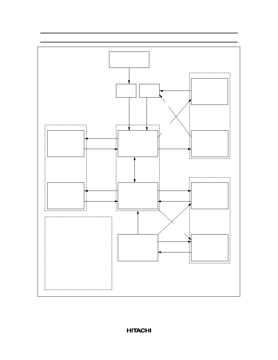
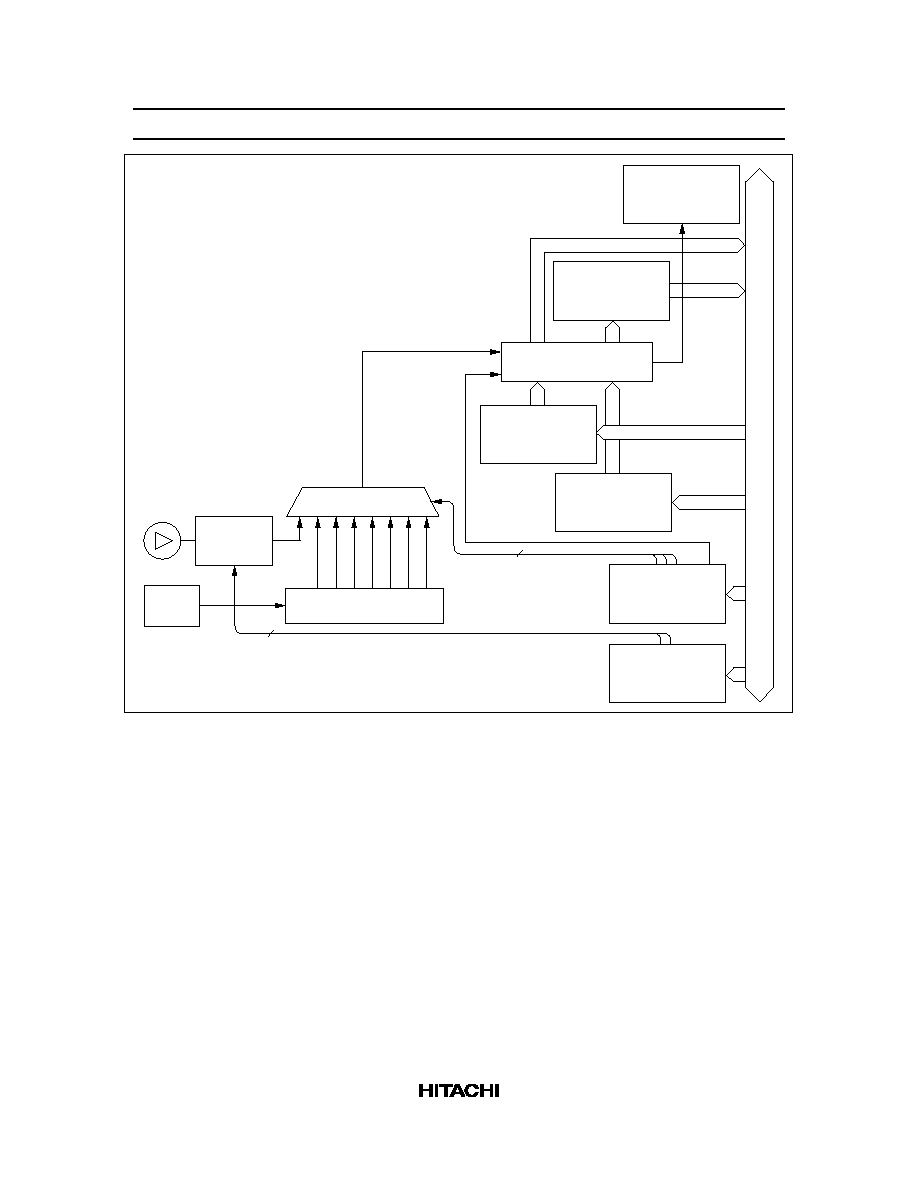
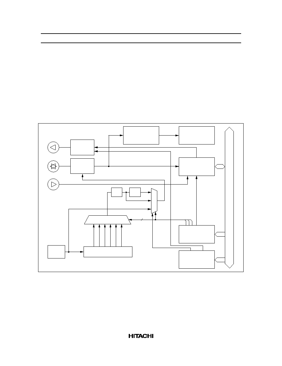
Block Diagram
D
0
D
1
D
2
D
3
D
4
D
5
D
6
D
7
D
8
D
9
D
10
D
11
D
12
D
13
R0
0
R0
1
R0
2
R0
3
D port
R0 port
R1
0
R1
1
R1
2
R1
3
R1 port
R2
0
R2
1
R2
2
R2
3
R2 port
R3
0
R3
1
R3
2
R3
3
R3 port
R4
0
R4
1
R4
2
R4
3
R4 port
R5
0
R5
1
R5
2
R5
3
R5 port
R6
0
R6
1
R6
2
R6
3
R6 port
R7
0
R7
1
R7
2
R7 port
R8
0
R8
1
R8
2
R8
3
R8 port
R9
0
R9
1
R9
2
R9
3
R9 port
RA
1
RA port
ROM
(16,384
◊
10 bits)
(12,288
◊
10 bits)
(8,192
◊
10 bits)
PC
(14 bits)
Instruction
decoder
SP
(10 bits)
B
(4 bits)
A
(4 bits)
ST
(1 bit)
CA
(1 bit)
ALU
SPY
(4 bits)
Y
(4 bits)
SPX
(4 bits)
X
(4 bits)
W
(4 bits)
RAM
(512
◊
4 bits)
System control
Interrupt
control
Timer A
Timer B
Timer C
Serial
interface
A/D
converter
Buzzer
Internal data bus
Internal data bus
Internal address bus
BUZZ
AV
CC
AN
11
AV
SS
AN
0
∑
∑
∑
∑
∑
∑
SI
SO
SCK
TOC
EVNB
INT
0
INT
1
Data bus
High voltage
pin
Directional
signal line
GND
V
CC
X2
X1
OSC
2
OSC
1
STOPC
TEST
RESET
(6,144
◊
10 bits)
(4,096
◊
10 bits)
HD404339 Series
9
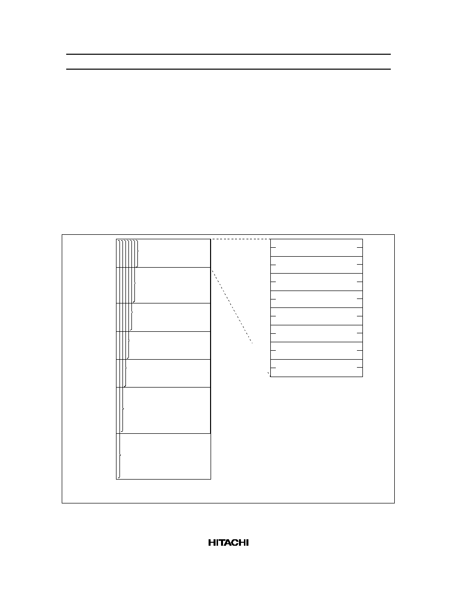
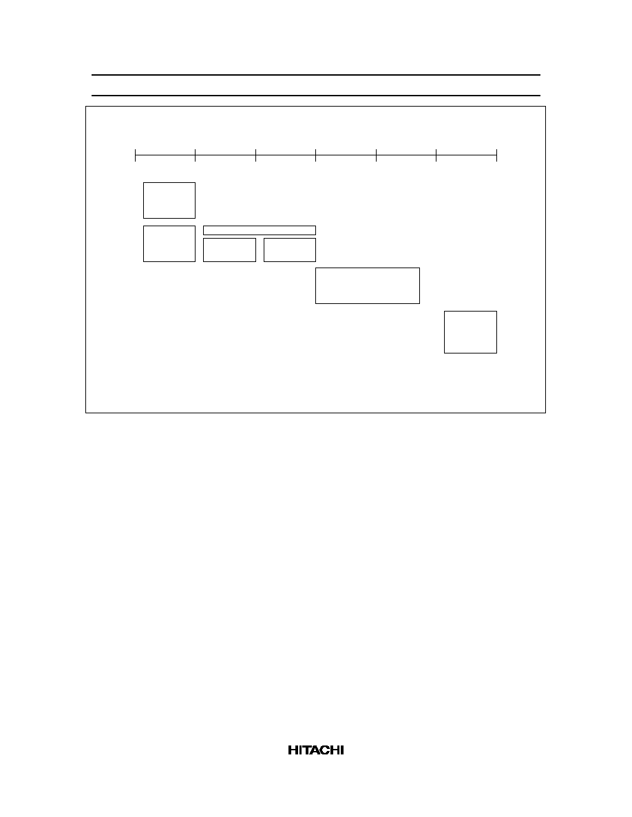
Memory Map
ROM Memory Map
Vector Address Area ($0000≠$000F): Reserved for JMPL instructions that branch to the start addresses
of the reset and interrupt routines.
Zero-Page Subroutine Area ($0000≠$003F): Reserved for subroutines. The program branches to a
subroutine in this area in response to the CAL instruction.
Pattern Area ($0000≠$0FFF): Contains ROM data that can be referenced with the P instruction.
Program Area ($0000-$0FFF (HD404334), $0000-$17FF (HD404336), $0000≠$1FFF (HD404338),
$0000≠$2FFF (HD4043312), $0000≠$3FFF (HD404339, HD4074339)): The entire ROM area can be
used for program coding.
$000F
$0FFF
$1000
$2FFF
$0010
$003F
$0040
Vector address
(16 words)
Zero-page subroutine
(64 words)
Pattern (4,096 words)
HD404334
Program (4,096 words)
HD404338
Program
(8,192 words)
$0000
$0000
$0001
$0002
$0003
$0004
$0005
$0006
$0007
$0008
$0009
$000A
$000B
$000C
$000D
$000E
$000F
0
1
JMPL instruction
(jump to
RESET
,
STOPC
routine)
JMPL instruction
(jump to
INT
routine)
JMPL instruction
(jump to timer A routine)
JMPL instruction
(jump to timer B routine)
JMPL instruction
(jump to timer C routine)
JMPL instruction
(jump to A/D converter routine)
JMPL instruction
(jump to
INT
routine)
JMPL instruction
(jump to serial routine)
HD4043312
Program
(12,288 words)
HD404339, HD4074339
Program
(16,384 words)
$1FFF
$2000
$3000
$3FFF
HD404336
Program
(6,144 words)
$17FF
$1800
Note:
Since the ROM address areas between $0000≠$0FFF overlap, the user can determine how these
areas are to be used.
Figure 1 ROM Memory Map
HD404339 Series
10
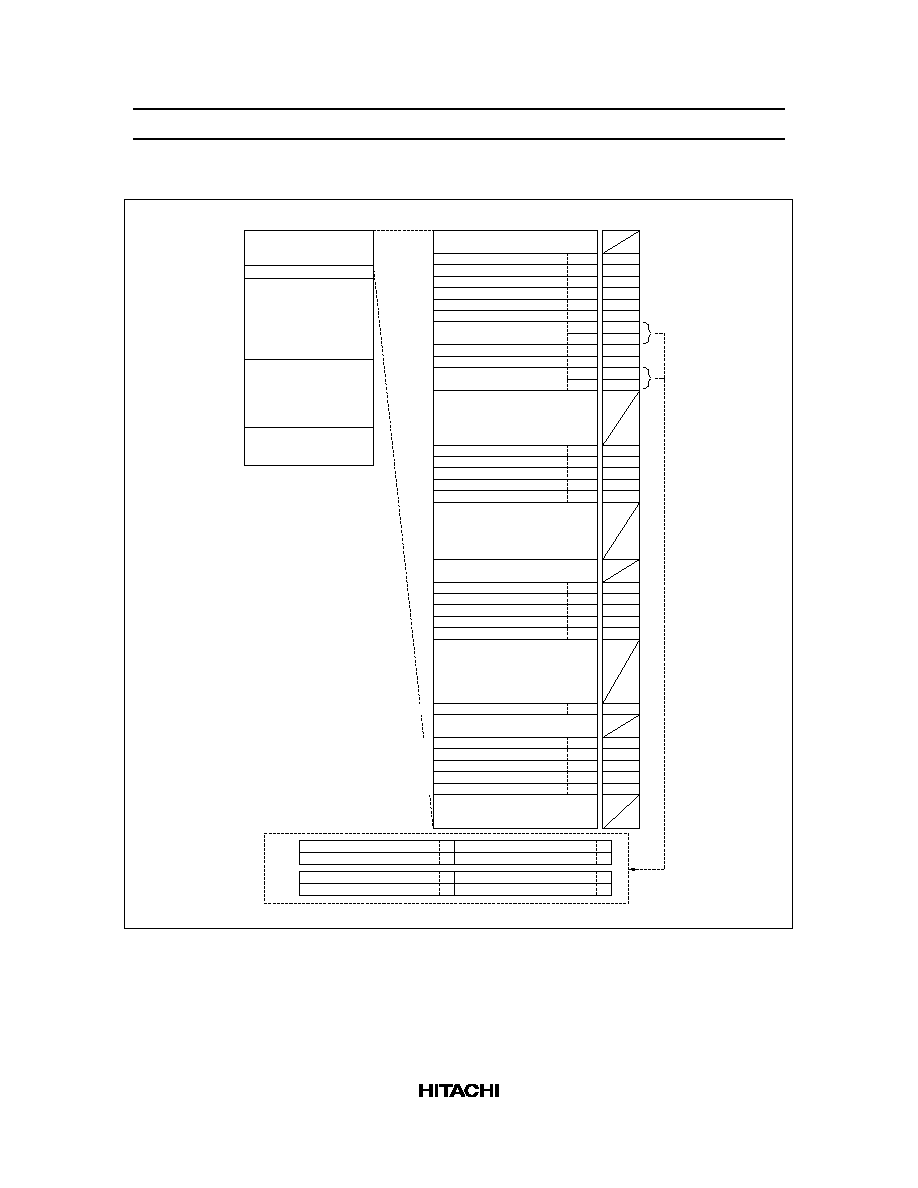
RAM Memory Map
A/D channel register (ACR)
$000
$000
$040
$050
$003
$004
$005
$006
$007
$008
$009
$00A
$00B
$00C
$00D
$00E
$00F
$020
$023
$033
$034
$035
$036
$037
$00A
$00B
$00E
$00F
W
W
R/W
W
W
W
W
W
W
W
W
W
R
R
R
R
W
R/W
R/W
R/W
R/W
R/W
$3C0
RAM-mapped registers
Memory registers (MR)
Stack (64 digits)
Interrupt control bits area
Port mode register A (PMRA)
Serial mode register (SMR)
Serial data register lower (SRL)
Serial data register upper (SRU)
Timer mode register A (TMA)
Timer mode register B1 (TMB1)
Timer B (TRBL/TWBL)
(TRBU/TWBU)
Miscellaneous register (MIS)
Timer mode register C (TMC)
Timer C (TRCL/TWCL)
(TRCU/TWCU)
Register flag area
Port R0 DCR (DCR0)
Port R3 DCR (DCR3)
Not used
1. Two registers are mapped
on the same area ($00A,
$00B, $00E, $00F).
2. Undefined.
Timer read register B lower (TRBL)
Timer read register B upper (TRBU)
Timer read register C lower (TRCL)
Timer read register C upper (TRCU)
Timer write register B lower (TWBL)
Timer write register B upper (TWBU)
Timer write register C lower (TWCL)
Timer write register C upper (TWCU)
R: Read only
W: Write only
R/W: Read/write
$200
Notes:
$016
R
A/D data register lower (ADRL)
$017
$024
$025
$026
$027
$028
$018
$019
$01A
$3FF
A/D data register upper (ADRU)
A/D mode register 1 (AMR1)
A/D mode register 2 (AMR2)
R
W
W
W
Port mode register B (PMRB)
Port mode register C (PMRC)
Timer mode register B2 (TMB2)
System clock selection register 1 (SSR1)
Not used
Port R4 DCR (DCR4)
Port R5 DCR (DCR5)
Port R6 DCR (DCR6)
Port R7 DCR (DCR7)
W
W
W
W
W
W
W
W
W
$030
Data (432 digits)
Not used
System clock selection register 2 (SSR2)
Not used
Not used
Not used
0000
0000
0000
Undefined
Undefined
0000
0000
*
2
/0000
0000
0000
0000
0000
0000
1000
0000
-000
0000
00-0
-000
000-
0000
0000
0000
-000
--00
Undefined
*
2
/0000
Undefined
*
1
Initial values
after reset
$03F
Figure 2 RAM Memory Map and Initial Values
HD404339 Series
11
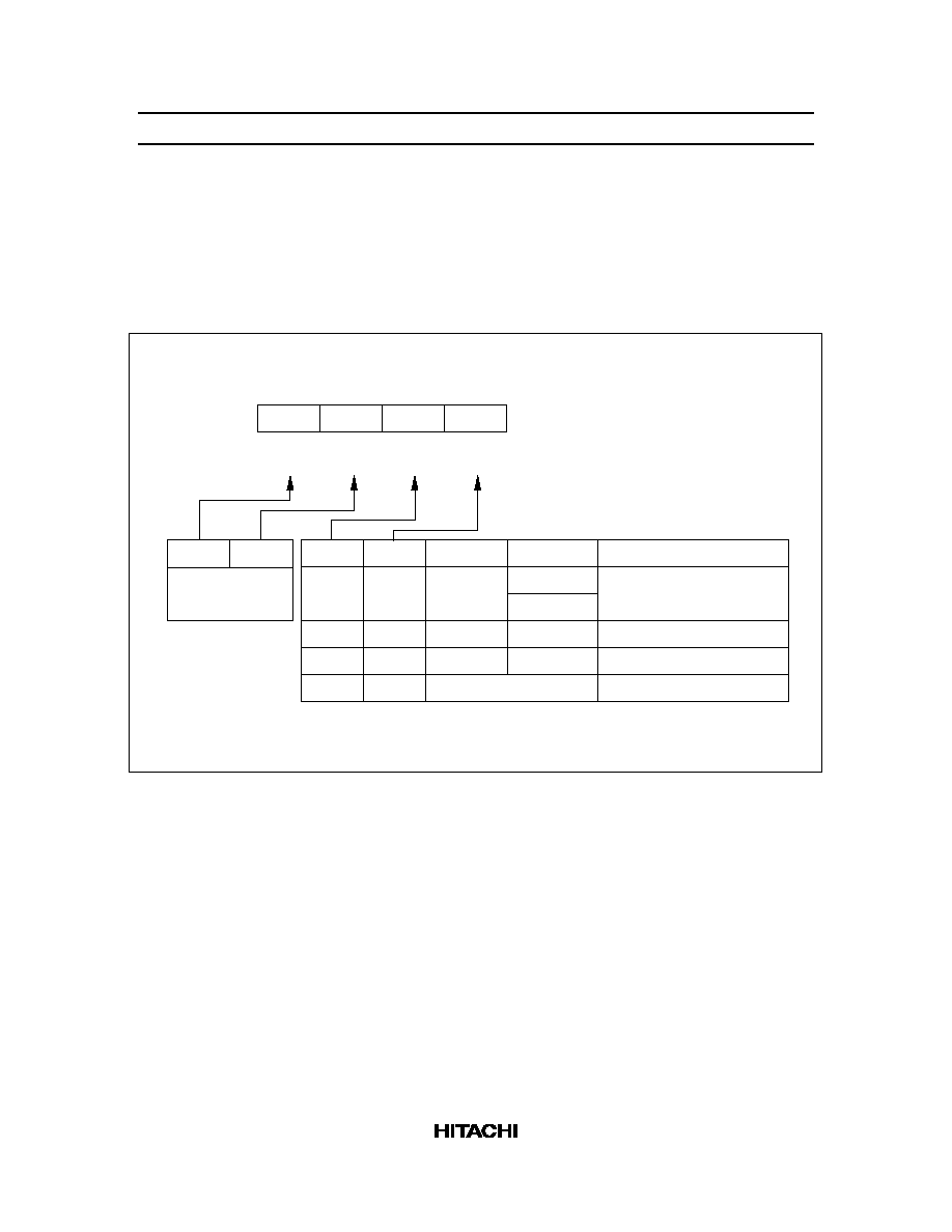
Table 1
Initial Values of Flags after MCU Reset
Item
Initial Value
Interrupt flags/mask
Interrupt enable flag (IE)
0
Interrupt request flag (IF)
0
Interrupt mask (IM)
1
Bit registers
Watchdog timer on flag (WDON)
0
A/D start flag (ADSF)
0
Input capture status flag (ICSF)
0
Input capture error flag (ICEF)
0
I
AD
off flag (IAOF)
0
RAM enable flag (RAME)
0
Low speed on flag (LSON)
0
Direct transfer on flag (DTON)
0
Bit 3
Bit 2
Bit 1
Bit 0
IMTA
(IM of timer A)
IFTA
(IF of timer A)
IM1
(IM of
INT
1
)
IF1
(IF of
INT
1
)
IMTC
(IM of timer C)
IFTC
(IF of timer C)
IMTB
(IM of timer B)
IFTB
(IF of timer B)
IMS
(IM of serial)
IFS
(IF of serial)
IMAD
(IM of A/D)
IFAD
(IF of A/D)
$0000
$0001
$0002
$0003
IM0
(IM of
INT
0
)
IF0
(IF of
INT
0
)
RSP
(Reset SP bit)
IE
(Interrupt
enable flag)
ICSF
(Input capture
status flag)
$020
$021
$022
$023
DTON
(Direct transfer
on flag)
ADSF
(A/D start flag)
WDON
(Watchdog
on flag)
LSON
(Low speed
on flag)
ICEF
(Input capture
error flag)
RAME
(RAM enable
flag)
IF: Interrupt
request flag
IM: Interrupt
mask
IE: Interrupt
enable flag
SP: Stack pointer
Bit 3
Bit 2
Bit 1
Bit 0
RAM Address
IAOF
(I
AD
off flag)
Not used
Interrupt control bits area
Register flag area
Figure 3 Interrupt Control Bits and Register Flag Areas Configuration
HD404339 Series
12
IE
IM
LSON
IAOF
IF
ICSF
ICEF
RAME
RSP
WDON
ADSF
DTON
Not used
SEM/SEMD
Not executed
Allowed
Allowed
REM/REMD
TM/TMD
Allowed
Allowed
Allowed
Not executed
Allowed
Allowed
Not executed in active mode
Used in subactive mode
Not executed
Allowed
Not executed
Inhibited
Allowed
Not executed
Inhibited
Inhibited
Allowed
Allowed
Inhibited
Note: WDON is reset by MCU reset or by STOPC enable for stop mode cancellation.
The REM or REMD instruction must not be executed for ADSF during A/D conversion.
DTON is always reset in active mode. If the TM or TMD instruction is executed for
the inhibited bits or non-existing bits, the value in ST becomes invalid.
Figure 4 Usage Limitations of RAM Bit Manipulation Instructions
Memory registers
$040
$041
$042
$043
$044
$045
$046
$047
$048
$049
$04A
$04B
$04C
$04D
$04E
$04F
$3C0
$3FF
MR(0)
MR(1)
MR(2)
MR(3)
MR(4)
MR(5)
MR(6)
MR(7)
MR(8)
MR(9)
Level 16
Level 15
Level 14
Level 13
Level 12
Level 11
Level 10
Level 9
Level 8
Level 7
Level 6
Level 5
Level 4
Level 3
Level 2
Level 1
MR(10)
MR(11)
MR(12)
MR(13)
MR(14)
MR(15)
PC
PC
PC
PC
PC
PC
PC
PC
PC
PC
PC
PC
ST
PC
CA
PC
10
3
13
9
6
2
12
8
5
1
11
7
4
0
Bit 3
Bit 2
Bit 1
Bit 0
PC ≠PC :
ST: Status flag
CA: Carry flag
Program counter
13
Stack area
0
$3FC
$3FD
$3FE
$3FF
Figure 5 Configuration of Memory Registers and Stack Area, and Stack Position

HD404339 Series
13
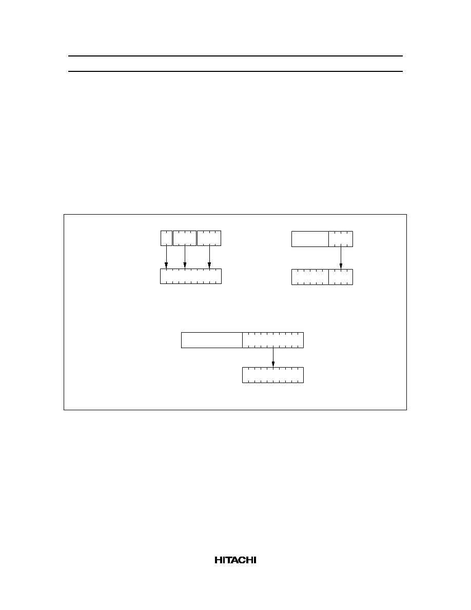
Registers and Flags
3
0
3
0
3
0
3
0
3
0
3
0
0
0
0
13
9
5
1
(B)
(A)
(W)
(X)
(Y)
(SPX)
(SPY)
(CA)
(ST)
(PC)
(SP)
1
1
1
1
Accumulator
B register
W register
X register
Y register
SPX register
SPY register
Carry
Status
Program counter
Initial value: 0,
no R/W
Stack pointer
Initial value: $3FF, no R/W
0
0
Initial value: Undefined, R/W
Initial value: Undefined, R/W
Initial value: Undefined, R/W
Initial value: Undefined, R/W
Initial value: Undefined, R/W
Initial value: Undefined, R/W
Initial value: Undefined, R/W
Initial value: Undefined, R/W
Initial value: 1, no R/W
Figure 6 Registers and Flags
HD404339 Series
14
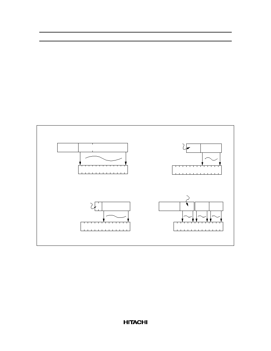
Addressing Modes
RAM Addressing Modes
Register Indirect Addressing Mode: The contents of the W, X, and Y registers (10 bits total) are used as
a RAM address.
Direct Addressing Mode: A direct addressing instruction consists of two words. The first word contains
the opcode, and the contents of the second word (10 bits) are used as a RAM address.
Memory Register Addressing Mode (LAMR, XMRA): The memory registers (MR), which are located
in 16 addresses from $040 to $04F, are accessed with the LAMR and XMRA instructions.
0
0
9
9
Opcode
Register Indirect Addressing
2nd instruction
word
RAM address
Direct Addressing
Instruction
9
0
0
9
RAM address
1st instruction
word
3
7
3
0
Memory Register Addressing
0
9
RAM address 0 0 0 1 0 0
Opcode
Instruction
3
0 3
0
0
1
W
X
Y
Figure 7 RAM Addressing Modes
HD404339 Series
15
ROM Addressing Modes
Direct Addressing Mode: A program can branch to any address in ROM memory space by executing the
JMPL, BRL, or CALL instruction.
Current Page Addressing Mode: A program can branch to any address in the current page (256 words
per page) by executing the BR instruction.
Zero-Page Addressing Mode: A program can branch to any subroutine located in the zero-page
subroutine area ($0000≠$003F) by executing the CAL instruction.
Table Data Addressing Mode: A program can branch to an address determined by the contents of 4-bit
immediate data, the accumulator, and the B register by executing the TBR instruction.
0
0
Direct Addressing
2nd
instruction word
Program counter
Current Page Addressing
9
7
0
9
Program counter
1st
instruction word
5
0
Zero-Page Addressing
0 0
Operand
0
9
Table Data Addressing
7
13
0
9
Operand
Opcode
3
0
13
Operand
* * * * * *
Opcode
Program counter
0
13
3
Operand
Opcode
B
A
0
9
Opcode
0 0 0 0 0 0 0 0
Program counter
0
13
Figure 8 ROM Addressing Modes

HD404339 Series
16
Instruction Set
Table 2
Instruction Set Classification
Instruction Type
Function
Number of
Instructions
Immediate
Transferring constants to the accumulator, B register, and RAM.
4
Register-to-register
Transferring contents of the B, Y, SPX, SPY, or memory registers to
the accumulator.
8
RAM addressing
Available when accessing RAM in register indirect addressing
mode.
13
RAM register
Transferring data between the accumulator and memory.
10
Arithmetic
Performing arithmetic operations with the contents of the
accumulator, B register, or memory.
25
Compare
Comparing contents of the accumulator or memory with a constant.
12
RAM bit manipulation
Bit set, bit reset, and bit test.
6
ROM addressing
Branching and jump instructions based on the status condition.
8
Input/output
Controlling the input/output of the R and D ports; ROM data
reference with the P instruction.
11
Control
Controlling the serial communication interface and low-power
dissipation modes.
4
Total: 101
instructions
HD404339 Series
17
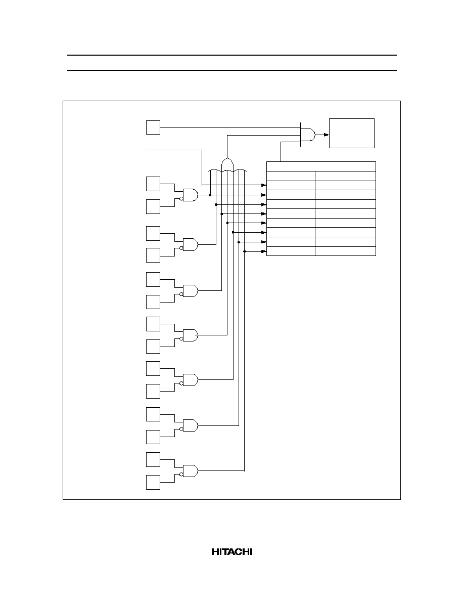
Interrupts
IE
IF0
IM0
IF1
IM1
IFTA
IMTA
IFTB
IMTB
IFTC
IMTC
IFAD
IMAD
$000,0
$000,2
$000,3
$001,0
$001,1
$001,2
$001,3
$002,0
$002,1
$002,2
$002,3
$003,0
$003,1
Interrupt
request
Priority Controller
IFS
IMS
$003,2
$003,3
INT
0
interrupt
INT
1
interrupt
Timer A interrupt
Timer B interrupt
Timer C interrupt
A/D interrupt
Serial interrupt
Priority Order
Vector Address
1
2
3
4
5
6
7
$0000
$0002
$0004
$0006
$0008
$000A
$000C
$000E
(
RESET
,
STOPC
)
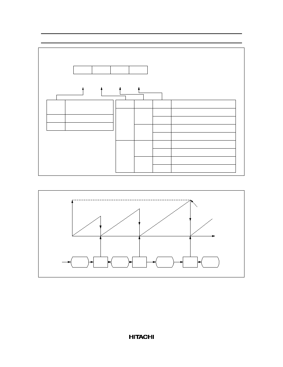
Figure 9 Interrupt Control Circuit
HD404339 Series
18
Instruction cycles
1
2
3
4
5
6
Instruction
execution
*
Interrupt
acceptance
Execution of JMPL
instruction at vector address
Execution of
instruction at
start address
of interrupt
routine
IE reset
Vector address
generation
Stacking
Note:
*
The stack is accessed and the interrupt enable flag is reset after the instruction
is executed, even if it is a two-cycle instruction.
Figure 10 Interrupt Processing Sequence

HD404339 Series
19
Operating Modes
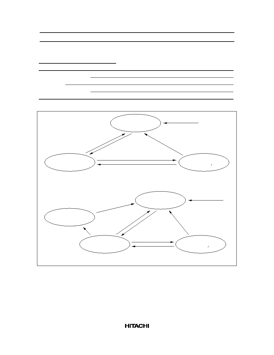
The MCU has five operating modes as shown in table 3. Transitions between operating modes are shown
in figure 11.
Table 3
Operations in Each Operating Mode
Function
Active Mode
Subactive
Mode
Standby Mode
Watch Mode
Stop Mode
System oscillator
OP
Stopped
OP
Stopped
Stopped
Subsystem oscillator OP
OP
OP
OP
*
OP
CPU
OP
OP
Retained
Retained
Reset
RAM
OP
OP
Retained
Retained
Retained
Timer A
OP
OP
OP
OP
Reset
Timers B, C
OP
OP
OP
Stopped
Reset
Serial
OP
OP
OP
Stopped
Reset
A/D
OP
Stopped
OP
Stopped
Reset
I/O
OP
OP
Retained
Retained
Reset
Notes: OP
implies in operation.
*
Oscillation can be switched on or off with bit 3 of system clock selection register 1 (SSR1: $027).
HD404339 Series
20
Reset by
RESET
input or
by watchdog timer
f
OSC
:
f
X
:
¯
CPU
:
¯
CLK
:
¯
PER
:
Oscillate
Oscillate
Stop
f
cyc
f
cyc
f
OSC
:
f
X
:
¯
CPU
:
¯
CLK
:
¯
PER
:
Oscillate
Oscillate
Stop
f
W
f
cyc
f
OSC
:
f
X
:
¯
CPU
:
¯
CLK
:
¯
PER
:
Oscillate
Oscillate
f
cyc
f
cyc
f
cyc
f
OSC
:
f
X
:
¯
CPU
:
¯
CLK
:
¯
PER
:
Oscillate
Oscillate
f
cyc
f
W
f
cyc
f
OSC
:
f
X
:
¯
CPU
:
¯
CLK
:
¯
PER
:
Stop
Oscillate
f
SUB
f
W
f
SUB
f
OSC
:
f
X
:
¯
CPU
:
¯
CLK
:
¯
PER
:
Stop
Stop
Stop
Stop
Stop
f
OSC
:
f
X
:
¯
CPU
:
¯
CLK
:
¯
PER
:
Stop
Oscillate
Stop
f
W
Stop
f
OSC
:
f
X
:
¯
CPU
:
¯
CLK
:
¯
PER
:
Stop
Oscillate
Stop
f
W
Stop
Standby mode
Stop mode
(TMA3 = 0, SSR13 = 1)
Watch mode
Subactive
mode
(TMA3 = 1)
(TMA3 = 1, LSON = 0)
(TMA3 = 1, LSON = 1)
SBY
instruction
Interrupt
SBY
instruction
Interrupt
STOP
instruction
INT
0
,
timer A
f
OSC
:
f
X
:
f
cyc
:
f
SUB
:
f
W
:
LSON:
DTON:
Main oscillation frequency
Subsystem oscillation
frequency for time base
f
OSC
/4, f
OSC
/8, f
OSC
/16,
or f
OSC
/32
(software selectable)
f
X
/8 or f
X
/4
(software selectable)
f
X
/8
System clock
Clock for timer A
Clock for other peripheral
functions (except timer A)
Low speed on flag
Direct transfer on flag
Active
mode
¯
CPU
:
¯
CLK
:
¯
PER
:
f
OSC
:
f
X
:
¯
CPU
:
¯
CLK
:
¯
PER
:
Stop
Oscillate
Stop
Stop
Stop
(TMA3 = 0, SSR13 = 0)
RESET 1
RESET 2
RAME = 0
RAME = 1
INT
0
,
timer A
(TMA3 = 0)
STOP
instruction
STOPC
STOPC
STOP
instruction
1. STOP/SBY (DTON = 1, LSON = 0)
2. STOP/SBY (DTON = 0, LSON = 0)
3. STOP/SBY (DTON = Don't care, LSON = 1)
Notes:
*
1
*
2
*
3
STOP
instruction
Figure 11 MCU Status Transitions

HD404339 Series
21
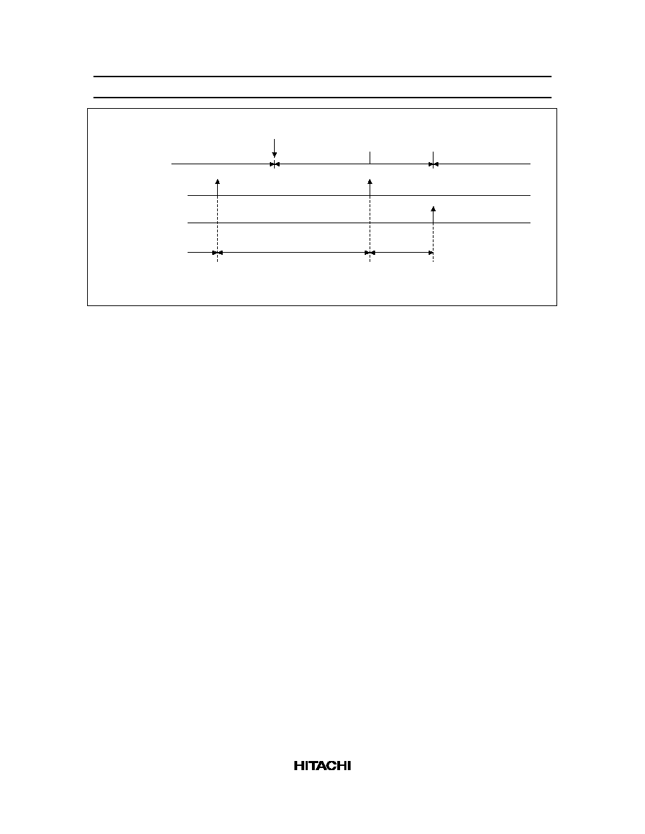
In stop mode, the system oscillator is stopped. To ensure a proper oscillation stabilization period of at least
t
RC
when clearing stop mode, execute the cancellation according to the timing chart in figure 12.
In watch and subactive modes, a timer A or
INT
0
interrupt can be accepted during the interrupt frame
period T (see figure 13).
Note:
In watch and subactive modes, an interrupt will not be properly detected if the
INT
0
high or low
level period is shorter than the interrupt frame period T. Thus, when operating in watch and
subactive modes, maintain the
INT
0
high or low level period longer than period T to ensure
interrupt detection.
,
,
,
,
Stop mode
Oscillator
Internal
clock
STOP instruction execution
t
res
t
RC
(stabilization period)
t
res
�
�
RESET
or
STOPC
Figure 12 Timing of Stop Mode Cancellation
Active mode
Interrupt strobe
Watch mode
Oscillation
stabilization
period
Active mode
T
t
RC
T:
t :
RC
Interrupt frame length
Oscillation stabilization period
INT
0
Interrupt request
generation
(During the transition
from watch mode to
active mode only)
Tx
T
T + t
RC
T
X
2T + t
RC
Figure 13 Interrupt Frame
HD404339 Series
22
The MCU automatically provides an oscillation stabilization period t
RC
when operation switches from
watch mode to active mode. The interrupt frame period T and one of three values for t
RC
can be selected
with the miscellaneous register (MIS: $00C), as listed in figure 14.
Operation can switch directly from subactive mode to active mode, as illustrated in figure 15. In this case,
the transition time T
D
obeys the following relationship.
t
RC
< T
D
< T + t
RC
Bit
Initial value
Read/Write
Bit name
3
0
W
MIS3
2
0
W
MIS2
0
0
W
MIS0
1
0
W
MIS1
Miscellaneous register (MIS: $00C)
MIS1
0
MIS0
T
*
1
0
0.24414 ms
t
RC
*
1
0.12207 ms
0.24414 ms
*
2
7.8125 ms
62.5 ms
Oscillation Circuit Conditions
External clock input
Ceramic oscillator
0
1
1
1
0
1
15.625 ms
125 ms
Not used
--
Notes: 1.
2.
The values of T and t
RC
are applied when a 32.768-kHz crystal oscillator is used.
The value is applied only when direct transfer operation is used.
Buffer control.
Refer to figure 24.
MIS3
MIS2
Crystal oscillator
Figure 14 Miscellaneous Register
HD404339 Series
23
Subactive mode
Interrupt strobe
Direct transfer
completion timing
MCU internal
processing period
Oscillation
stabilization
time
Active mode
T
t
RC
T:
t :
RC
STOP/SBY instruction execution
(Set LSON = 0, DTON = 1)
Interrupt frame period
Oscillation stabilization time
Figure 15 Direct Transition Timing
MCU Operation Sequence: The MCU operation flow is shown in figures 16 and 17.
RESET input is
asynchronous, and causes an immediate transition to the reset state from any MPU operation state.
The low-power mode operation sequence is shown in figure 17. With the IE flag cleared and an interrupt
flag set together with its interrupt mask cleared, if a STOP/SBY instruction is executed, the instruction is
cancelled (regarded as an NOP) and the following instruction is executed. Before executing a STOP/SBY
instruction, make sure all interrupt flags are cleared or all interrupts are masked.
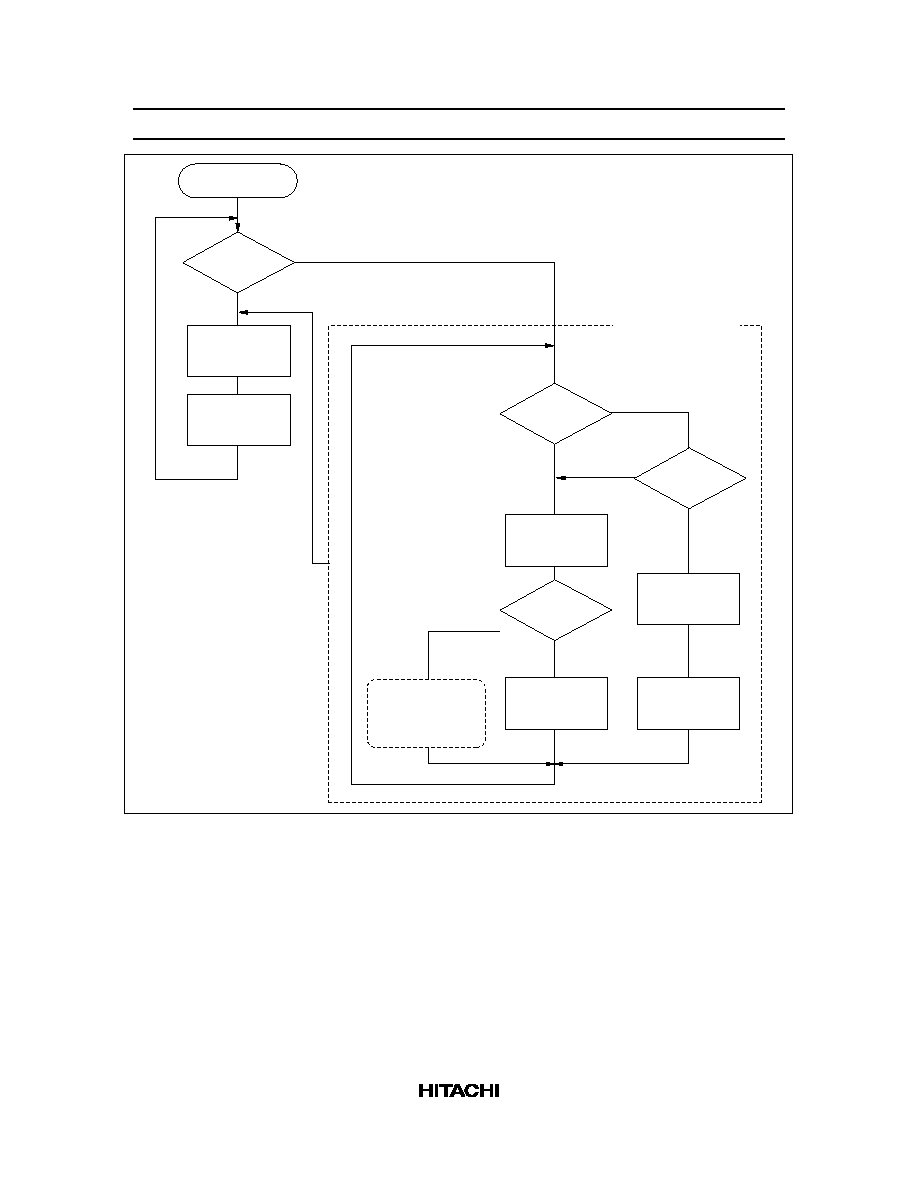
HD404339 Series
24
Power on
MCU reset
RAME = 0
IE
0
Stack
(PC),
(CA), (ST)
No
Yes
IF = 1?
RESET
= 0?
SBY/STOP
instruction
IM = 0
IE = 1
RAME = 1
Instruction
execution
Reset input
PC
vector
address
No
No
No
Yes
Yes
Yes
MCU operation cycle
PC
(PC)+1
Power-down mode
operation cycle
(see figure 17)
Figure 16 MCU Operation Sequence (Power On)

HD404339 Series
25
Low-power mode
operation cycle
IF = 1 and
IM = 0?
Hardware NOP
execution
PC Next
Iocation
MCU operation
cycle
Standby mode
IF = 1 and
IM = 0?
Hardware NOP
execution
PC Next
Iocation
Instruction
execution
Stop mode
No
Yes
No
Yes
STOPC
= 0?
RAME = 1
Reset MCU
No
Yes
Figure 17 MCU Operating Sequence (Low-Power Mode Operation)
HD404339 Series
26
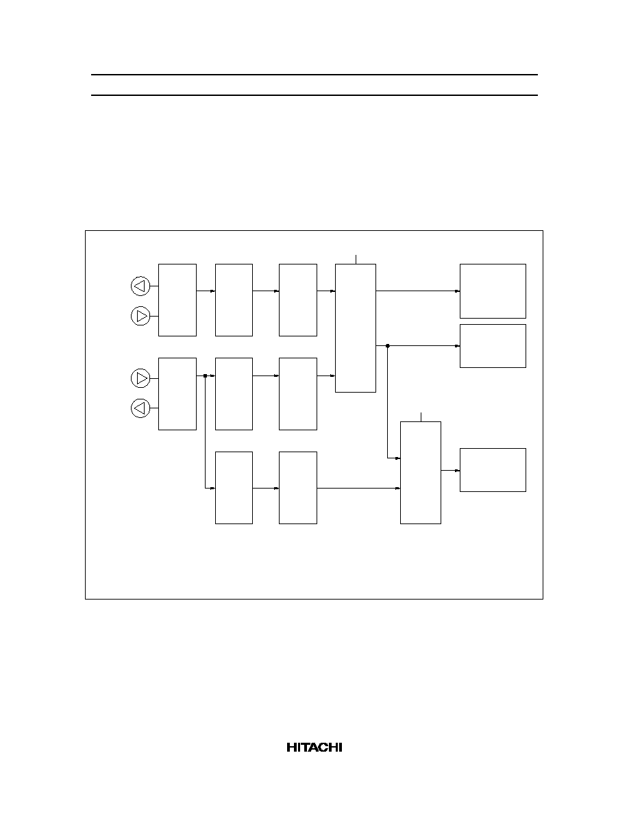
Oscillator Circuit
Figure 18 shows a block diagram of the clock generation circuit. The system clock frequency of the
oscillator connected to OSC
1
and OSC
2
can be selected by system clock selection registers 1 and 2 (SSR1,
2: $027, $028) as shown in figures 20 and 21.
The system clock division ratio can be set by software to be 1/4, 1/8, 1/16, or 1/32. The subsystem clock
division ratio can be set by software to be 1/4 or 1/8.
OSC
2
OSC
1
X1
X2
System
oscillator
Sub-
system
oscillator
1/4, 1/8,
1/16, or
1/32
division
circuit
Timing
generator
circuit
System
clock
selection
CPU with ROM,
RAM, registers,
flags, and I/O
Peripheral
function
interrupt
Time-base
interrupt
Time-base
clock
selection
1/8 or 1/4
division
circuit
Timing
generator
circuit
Timing
generator
circuit
1/8
division
circuit
f
W
f
SUB
t
subcyc
LSON
TMA3
f
cyc
t
cyc
f
OSC
f
X
t
Wcyc
¯
CPU
¯
PER
¯
CLK
Notes: 1.
2.
The system clock division ratio can be selected by setting bit 1 or 0 of the system
clock select register 2 (SSR2: $028).
The system clock division ratio can be selected by setting bit 2 of the system
clock select register 1 (SSR1: $027).
*
1
*
2
Figure 18 Clock Generation Circuit
HD404339 Series
27
OSC
2
X1
GND
OSC
1
RESET
X2
AV
SS
GND
Figure 19 Typical Layout of Crystal and Ceramic Oscillators
HD404339 Series
28
Table 4
Oscillator Circuit Examples
Circuit Configuration
Circuit Constants
External clock
operation
External
oscillator
OSC
Open
1
OSC
2
Ceramic oscillator
(OSC
1
, OSC
2
)
OSC
2
C
1
2
C
OSC
1
R
f
Ceramic
GND
Ceramic oscillator: CSA4.00MG
(Murata)
R
f
= 1 M
±
20%
C
1
= C
2
= 30 pF
±
20%
Crystal oscillator
(OSC
1
, OSC
2
)
OSC
2
C
1
2
C
OSC
1
R
f
Crystal
GND
L
S
C
R
S
C
0
OSC
1
OSC
2
R
f
= 1 M
±
20%
C
1
= C
2
= 10 to 22 pF
±
20%
Crystal: Equivalent to circuit shown below
C
0
= 7 pF max.
R
S
= 100
max.
Crystal oscillator
(X1, X2)
X1
C
1
2
C
X2
Crystal
GND
L
S
C
R
S
C
0
X1
X2
Crystal: 32.768 kHz: MX38T (Nippon
Denpa)
C
1
= C
2
= 20 pF
±
20%
R
S
= 14 k
C
0
= 1.5 pF
Notes: 1. Since the circuit constants change depending on the crystal or ceramic oscillator and stray
capacitance of the board, the user should consult with the crystal or ceramic oscillator
manufacturer to determine the circuit parameters.
2. Wiring among OSC
1
, OSC
2
, X1, X2 and elements should be as short as possible, and must not
cross other wiring (see figure 19).
3. When a 32.768-kHz crystal oscillator is not used, fix pin X1 to GND and leave pin X2 open.

HD404339 Series
29
Bit
Initial value
Read/Write
Bit name
3
0
W
SSR13
*
1
2
0
W
SSR12
0
--
--
Not used
1
0
W
SSR11
System clock selection register 1 (SSR1: $027)
System Clock Selection
*
2
0.4 to 1.0 MHz
1.6 to 4.5 MHz
SSR11
0
1
SSR12
0
1
Ratio Selection
f
SUB
= f
X
/8
f
SUB
= f
X
/4
32-kHz Oscillation Division
SSR13
0
1
32-kHz Oscillation Stop
Oscillation operates in stop mode
Oscillation stops in stop mode
Notes:
*
1
*
2
SSR13 will only be cleared to 0 by a
RESET
input. A
STOPC
input during stop mode will not
clear SSR13. Also note that SSR13 will not be cleared upon transition to stop mode.
When the subsystem oscillator (32.768 kHz crystal oscillator) is used, set 0.4 MHz
f
OSC
1.0MHz
or 1.6 MHz
f
OSC
4.5 MHz.
Figure 20 System Clock Selection Register 1 (SSR1)
Bit
Initial value
Read/Write
Bit name
3
--
--
Not used
2
--
--
Not used
0
0
W
SSR20
1
0
W
SSR21
System clock selection register 2 (SSR2: $028)
SSR21
0
0
1
1
SSR20
0
1
0
1
System Clock Division Ratio
1/4 division
1/8 division
1/16 division
1/32 division
Figure 21 System Clock Selection Register 2 (SSR2)

HD404339 Series
30
I/O Ports
The MCU has 53 input/output pins (D
0
≠D
13
, R0
0
≠R9
3
) and one input-only pin (RA
1
).
∑
The 30 pins consisting of ports D
0
≠D
13
, R1, R2, R8, and R9 are all high-voltage I/O pins. RA
1
is a high-
voltage input-only pin. The high-voltage pins can be equipped with or without pull-down resistance, as
selected by the mask option.
∑
All standard voltage output pins are CMOS output pins. However, the R0
2
/SO pin can be programmed
for NMOS open-drain output.
∑
In stop mode, input/output pins go to the high-impedance state.
∑
All standard voltage input/output pins have pull-up MOS built in, which can be individually turned on
or off by software (Table 5).
Pull-up MOS on/off settings can be made independently of settings as on-chip supporting module pins.
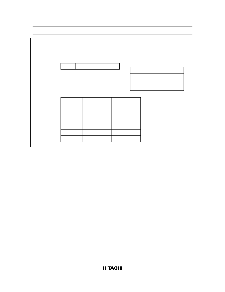
Table 5
Control of Standard I/O Pins by Program
MIS3 (bit 3 of MIS)
0
1
DCR
0
1
0
1
PDR
0
1
0
1
0
1
0
1
CMOS buffer
PMOS
--
--
--
On
--
--
--
On
NMOS
--
--
On
--
--
--
On
--
Pull-up MOS
--
--
--
--
--
On
--
On
Note:
-- indicates off.
HD404339 Series
31
Bit
Initial value
Read/Write
Bit name
3
0
W
DCR03,
2
0
W
DCR02,
0
0
W
DCR00,
1
0
W
DCR01,
DCR0, DCR3
to DCR7
Data control register
(DCR0: $030, DCR3 to DCR7: $033 to $037)
DCR33
to
DCR63
DCR32
to
DCR72
DCR30
to
DCR70
DCR31
to
DCR71
Bits 0 to 3
0
CMOS Buffer Control
CMOS buffer off
(high impedance)
CMOS buffer on
Register
DCR0
DCR3
DCR4
DCR5
DCR6
DCR7
Bit 3
R0
3
R3
3
R4
3
R5
3
R6
3
Not used
Correspondence between ports and DCR bits
Bit 2
R0
2
R3
2
R4
2
R5
2
R6
2
R7
2
Bit 1
R0
1
R3
1
R4
1
R5
1
R6
1
R7
1
Bit 0
R0
0
R3
0
R4
0
R5
0
R6
0
R7
0
1
Figure 22 Data Control Register (DCR)

HD404339 Series
32
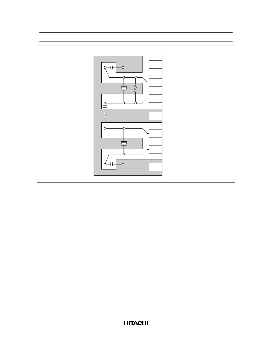
Table 6
Circuit Configurations of Standard I/O Pins
I/O Pin Type
Circuit
Pins
Input/output pins
V
CC
V
CC
Pull-up control signal
Buffer control
signal
Output data
Input data
HLT
MIS3
PDR
Input control signal
DCR
R0
0
, R0
1
, R0
3
,
R3
0
≠R3
3
,
R4
0
≠R4
3
,
R5
0
≠R5
3
,
R6
0
≠R6
3
,
R7
0
≠R7
2
V
CC
V
CC
Pull-up control signal
Buffer control
signal
Output data
Input data
HLT
MIS3
DCR
PDR
Input control signal
MIS2
R0
2
Peripheral function
pins
Input/
output
pins
V
CC
V
CC
Pull-up control signal
Output data
Input data
HLT
MIS3
SCK
SCK
SCK
Output
pins
V
CC
V
CC
Pull-up control signal
PMOS control
signal
Output data
HLT
MIS3
SO
MIS2
SO
V
CC
V
CC
Pull-up control signal
Output data
HLT
MIS3
TOC
TOC
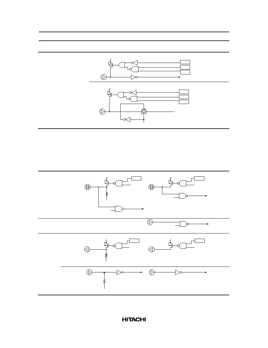
HD404339 Series
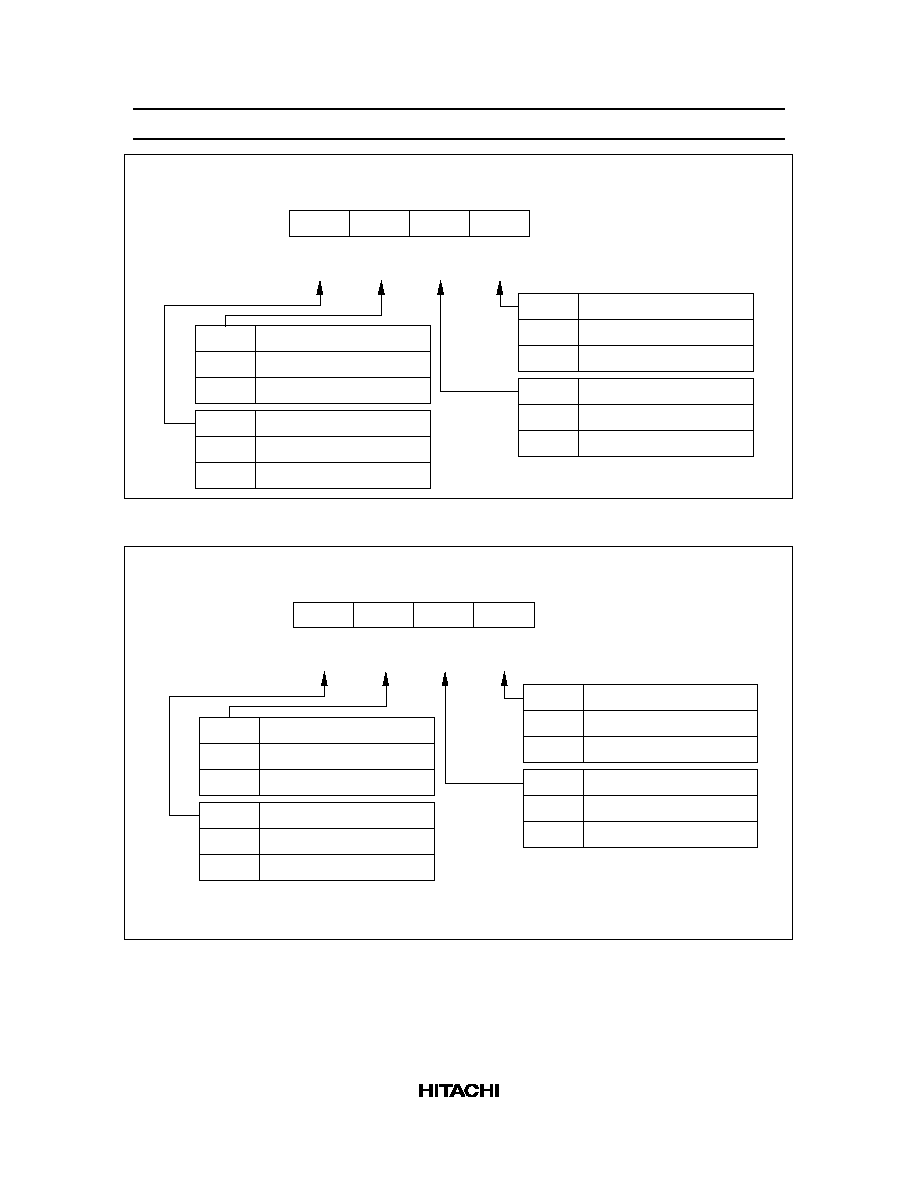
33
I/O Pin Type
Circuit
Pins
Peripheral function
pins
Input/
pins
V
CC
Input data
HLT
MIS3
SI
PDR
SI
Input control
V
CC
HLT
MIS3
PDR
A/D input
AN
0
≠AN
11
Notes: 1. In stop mode, the MCU is reset and the peripheral function selection is cancelled. The
HLT
signal goes low, and input/output pins enter the high-impedance state.
2. The
HLT
signal is 1 in active, standby, watch, and subactive modes.
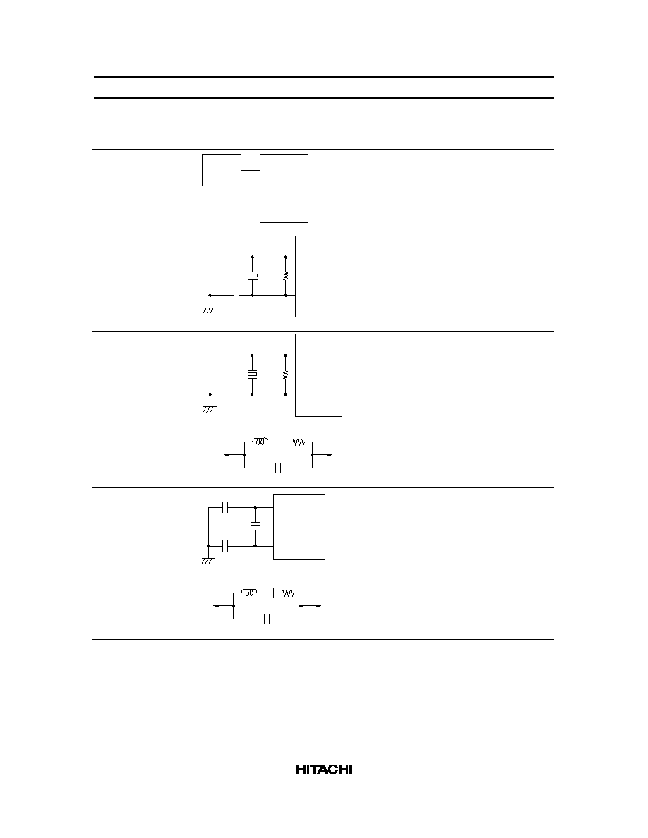
Table 7
Circuit Configurations for High-Voltage Input/Output Pins
I/O Pin Type
With Pull-Down Resistance
Without Pull-Down Resistance
Pins
Input/output
pins
V
CC
Input data
Input control
signal
HLT
Output
data
V
disp
Pull-down
resistance
V
CC
Input data
Input control
signal
Output
data
HLT
D
0
≠D
13
,
R1
0
≠R1
3
,
R2
0
≠R2
3
,
R8
0
≠R8
3
,
R9
0
≠R9
3
Input pins
Input data
Input control
signal
RA
1
Peripheral
function
pins
Output pins
V
CC
Output
data
V
disp
Pull-down
resistance
HLT
V
CC
Output
data
HLT
BUZZ
Input pins
Input data
Pull-down
resistance
V
disp
Input data
INT
0
,
INT
1
,
EVNB,
STOPC
Note:
HLT
goes high in active, standby, watch, and subactive modes.
HD404339 Series
34
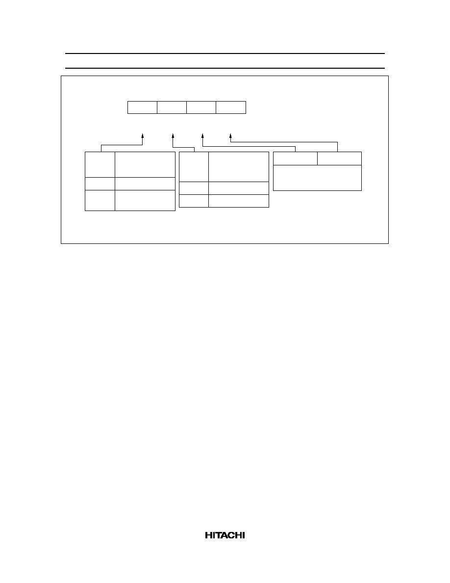
Bit
Initial value
Read/Write
Bit name
3
0
W
PMRA3
2
0
W
PMRA2
0
0
W
PMRA0
1
0
W
PMRA1
PMRA0
0
1
R0
2
/SO Mode Selection
R0
2
SO
Port mode register A (PMRA: $004)
PMRA1
0
1
R0
1
/SI Mode Selection
R0
1
SI
PMRA2
0
1
R0
3
/TOC Mode Selection
R0
3
TOC
PMRA3
0
1
D
3
/BUZZ Mode Selection
D
3
BUZZ
Figure 23 Port Mode Register A (PMRA)
Bit
Initial value
Read/Write
Bit name
3
0
W
PMRB3
2
0
W
PMRB2
0
0
W
PMRB0
1
0
W
PMRB1
PMRB0
0
1
D
0
/
INT
0
Mode Selection
D
0
INT
0
Port mode register B (PMRB: $024)
PMRB1
0
1
D
1
/
INT
1
Mode Selection
D
1
INT
1
PMRB2
0
1
D
2
/EVNB Mode Selection
D
2
EVNB
PMRB3
0
1
D
4
/
STOPC
Mode Selection
D
4
STOPC
*
Note:
PMRB3 is reset to 0 only by
RESET
input. When
STOPC
is input in stop mode, PMRB3 is not
reset but retains its value.
*
Figure 24 Port Mode Register B (PMRB)
HD404339 Series
35
Bit
Initial value
Read/Write
Bit name
3
0
W
MIS3
2
0
W
MIS2
0
0
W
MIS0
1
0
W
MIS1
MIS2
CMOS Buffer
On/Off Selection
for Pin R0
2
/SO
Miscellaneous register (MIS: $00C)
0
1
CMOS on
CMOS off
Refer to figure 14 in the
operation modes section.
t
RC
selection.
MIS3
0
1
Pull-Up MOS
On/Off Selection
Pull-up MOS off
Pull-up MOS on
(refer to table 5)
MIS1
MIS0
Note: The on/off status of each transistor and the peripheral function mode of each pin can be
set independently.
Figure 25 Miscellaneous Register

HD404339 Series
36
Prescaler
The MCU has two built-in prescalers, S and W (PSS, PSW). They divide the system clock and subsystem
clock, and output these divided clocks to the peripheral function modules, as shown in figure 26.
Subsystem
clock
Prescaler W
Timer A
Timer B
Timer C
Serial
System
clock
Prescaler S
Clock
selector
f
X
/8
f
X
/4 or f
X
/8
Figure 26 Prescaler Output Supply

HD404339 Series
37
Timers
The MCU has three built-in timers A, B, and C. The functions of each timer are listed in table 7.
Timer A
Timer A is an 8-bit free-running timer that can also be used as a clock time-base with a 32.768-kHz
subsystem oscillator. Timer A has the following features:
∑
One of eight internal clocks can be selected from prescaler S according to the setting of timer mode
register A (TMA: $008)
∑
In time-base mode, one of five internal clocks can be selected from prescaler W according to the setting
of timer mode register A
∑
An interrupt request can be generated when timer counter A (TCA) overflows
∑
Input clock frequency must not be modified during timer A operation
Table 7
Timer Functions
Functions
Timer A
Timer B
Timer C
Clock source
Prescaler S
Available
Available
Available
Prescaler W
Available
--
--
External event
--
Available
--
Timer functions
Free-running
Available
Available
Available
Time base
Available
--
--
Event counter
--
Available
--
Reload
--
Available
Available
Watchdog
--
--
Available
Input capture
--
Available
--
Timer output
PWM
--
--
Available

HD404339 Series
38
1/4
1/2
32.768-kHz
oscillator
System
clock
Prescaler W
(PSW)
Selector
Selector
Prescaler S (PSS)
Selector
Internal data bus
Timer A interrupt
request flag
(IFTA)
Clock
Overflow
Timer
counter A
(TCA)
Timer mode
register A
(TMA)
3
2 f
1/2 t
Wcyc
f
t
Wcyc
¯
PER
2
4
8
32
128
512
1024
2048
˜ ˜ ˜ ˜ ˜ ˜ ˜ ˜
2
8
16
32
˜ ˜ ˜ ˜
W
W
Figure 27 Timer A Block Diagram

HD404339 Series
39
Bit
Initial value
Read/Write
Bit name
3
0
W
TMA3
2
0
W
TMA2
0
0
W
TMA0
1
0
W
TMA1
Timer mode register A (TMA: $008)
0
0
1
0
0
1
0
1
0
1
0
1
0
1
0
1
0
1
PSS
PSS
PSS
PSS
PSS
PSS
PSS
PSS
PSW
PSW
PSW
PSW
PSW
Operating Mode
Timer A mode
TMA3
TMA1
TMA2
TMA0
Source
Prescaler
2048 t
cyc
1024 t
cyc
512 t
cyc
128 t
cyc
32 t
cyc
8 t
cyc
4 t
cyc
2 t
cyc
Input Clock
Frequency
0
1
1
32t
16t
8t
2t
1/2t
Time-base
mode
0
0
1
1
0
1
1
Not used
PSW and TCA reset
X
Notes:
Wcyc
Wcyc
Wcyc
Wcyc
Wcyc
X = Don't care.
1.
2.
3.
t = 244.14
µ
s (when a 32.768-kHz crystal oscillator is used)
Timer counter overflow output period (seconds) = input clock period (seconds) 256.
The division ratio must not be modified during time-base mode operation,
otherwise an overflow cycle error will occur.
Wcyc
◊
Figure 28 Timer Mode Register A (TMA)

HD404339 Series
40
Timer B
Timer B is an 8-bit multifunction timer that includes free-running, reload, and input capture timer features.
These are described as follows.
∑
By setting timer mode register B1 (TMB1: $009), one of seven internal clocks supplied from prescaler
S can be selected, or timer B can be used as an external event counter
∑
By setting timer mode register B2 (TMB2: $026), detection edge type of EVNB can be selected.
∑
By setting timer write register BL, U (TWBL, U: $00A, $00B), timer counter B (TCB) can be written
to during reload timer operation
∑
By setting timer read register BL, U (TRBL, U: $00A, $00B), the contents of timer counter B can be
read out
∑
Timer B can be used as an input capture timer to count the clock cycles between trigger edges input as
an external event
∑
An interrupt can be requested when timer counter B overflows or when a trigger input edge is received
during input capture operation
HD404339 Series
41
Timer counter B
(TCB)
Timer mode
register B2
(TMB2)
EVNB
Selector
System
clock
¯
PER
Prescaler S (PSS)
2
Edge
detector
Edge detection control signal
3
Timer write
register B lower
(TWBL)
Timer mode
register B1
(TMB1)
Timer write
register B upper
(TWBU)
Clock
Free-running
timer control
signal
Timer read
register B lower
(TRBL)
Interrupt request
flag of timer B
(IFTB)
Timer read
register BU
(TRBU)
Overflow
Internal data bus
2
4
8
32
128
512
2048
˜
˜
˜
˜
˜
˜
˜
Figure 29 Timer B Free-Running and Reload Operation Block Diagram
HD404339 Series
42
Timer counter B
(TCB)
Internal data bus
Timer mode
register B2
(TMB2)
EVNB
Selector
System
clock
PER
Prescaler S (PSS)
2
Edge
detector
Edge detection control signal
3
Timer mode
register B1
(TMB1)
Clock
Input capture
timer control
signal
Timer read
register B lower
(TRBL)
Interrupt request
flag of timer B
(IFTB)
Timer read
register BU
(TRBU)
Overflow
Read
signal
Input capture
status flag
(ICSF)
Input capture
error flag
(ICEF)
Error
controller
¯
2
4
8
32
128
512
2048
˜
˜
˜
˜
˜
˜
˜
Figure 30 Timer B Input Capture Operation Block Diagram

HD404339 Series
43
Bit
Initial value
Read/Write
Bit name
3
0
W
TMB13
2
0
W
TMB12
0
0
W
TMB10
1
0
W
TMB11
Timer mode register B1 (TMB1: $009)
0
1
0
1
0
1
0
1
0
1
0
1
0
1
2048t
cyc
512t
cyc
128t
cyc
32t
cyc
8t
cyc
4t
cyc
2t
cyc
TMB12
TMB10
TMB11
Input Clock Period and Input
Clock Source
D
2
/EVNB (External event input)
TMB13
0
1
Free-Running/Reload
Timer Selection
Free-running timer
Reload timer
Figure 31 Timer Mode Register B1 (TMB1)
Bit
Initial value
Read/Write
Bit name
3
--
--
Not used
2
0
W
TMB22
0
0
W
TMB20
1
0
W
TMB21
Timer mode register B2 (TMB2: $026)
TMB21
0
1
TMB20
0
1
0
1
EVNB Edge Detection Selection
No detection
Falling edge detection
Rising edge detection
Rising and falling edge detection
TMB22
0
1
Free-Running/Reload and Input Capture Selection
Free-Running/Reload
Input Capture
Figure 32 Timer Mode Register B2 (TMB2)

HD404339 Series
44
Timer C
Timer C is an 8-bit multifunction timer that includes free-running, reload, and watchdog timer features,
which are described as follows.
∑
By setting timer mode register C (TMC: $00D), one of eight internal clocks supplied from prescaler S
can be selected
∑
By selecting pin TOC with bit 2 (PMRA2) of port mode register A (PMRA: $004), timer C output
(PWM output) is enabled
∑
By setting timer write register CL, U (TWCL, U: $00E, $00F), timer counter C (TCC) can be written to
∑
By setting timer read register CL, U (TRCL, U: $00E, $00F), the contents of timer counter C can be
read out
∑
An interrupt can be requested when timer counter C overflows
∑
Timer counter C can be used as a watchdog timer for detecting runaway programs
HD404339 Series
45
Timer counter C
(TCC)
Port mode
register A (PMRA)
Selector
System
clock
PER
Prescaler S (PSS)
3
Timer write
register C lower
(TWCL)
Timer mode
register C (TMC)
Timer write
register C upper
(TWCU)
Clock
Free-running
timer control
signal
Timer read
register C lower
(TRCL)
Interrupt request
flag of timer C
(IFTC)
Timer read register CU (TRCU)
Overflow
TOC
Timer
output
control
signal
Watchdog timer
controller
Watchdog on
flag (WDON)
System reset signal
Internal data bus
Timer output
control logic
¯
2
4
8
32
128
512
1024
2048
˜
˜
˜
˜
˜
˜
˜
˜
Figure 33 Timer C Block Diagram
HD404339 Series
46
Bit
Initial value
Read/Write
Bit name
3
0
W
TMC3
2
0
W
TMC2
0
0
W
TMC0
1
0
W
TMC1
Timer mode register C (TMC: $00D)
0
1
0
1
0
1
0
1
0
1
0
1
0
1
2048t
cyc
512t
cyc
128t
cyc
32t
cyc
8t
cyc
4t
cyc
2t
cyc
TMC2
TMC0
TMC1
Input Clock Period
TMC3
0
1
Free-Running/Reload
Timer Selection
Free-running timer
Reload timer
1024t
cyc
Figure 34 Timer Mode Register C (TMC)
$FF + 1
$00
Timer C
count value
Overflow
Time
CPU
operation
Normal
operation
Timer C
clear
Normal
operation
Timer C
clear
Program
runaway
Normal
operation
Reset
Figure 35 Watchdog Timer Operation Flowchart
HD404339 Series
47
T (N + 1)
T 256
T
T (256 ≠ N)
◊
◊
◊
TMC3 = 0
(Free-running
timer)
TMC3 = 1
(Reload timer)
Notes: T: Input clock period supplied to counter.
(The clock source and system clock division ratio are determined by timer mode register C.)
N: Value of timer write register C. (When N = 255 ($FF), PWM output is fixed low.)
Figure 36 PWM Output Waveform

HD404339 Series
48
Notes on Use
When using the timer output as PWM output, note the following point. From the update of the timer write
register until the occurrence of the overflow interrupt, the PWM output differs from the period and duty
settings, as shown in table 8. The PWM output should therefore not be used until after the overflow
interrupt following the update of the timer write register. After the overflow, the PWM output will have the
set period and duty cycle.
Table 8
PWM Output Following Update of Timer Write Register
PWM Output
Mode
Timer Write Register is Updated during
High PWM Output
Timer Write Register is Updated during
Low PWM Output
Free running
Timer write
register
updated to
value N
Interrupt
request
T
◊
(255 ≠ N) T
◊
(N + 1)
Timer write
register
updated to
value N
Interrupt
request
T
◊
(N' + 1)
T
◊
(255 ≠ N)
T
◊
(N + 1)
Reload
Timer write
register
updated to
value N
Interrupt
request
T
T
◊
(255 ≠ N)
T
Timer write
register
updated to
value N
Interrupt
request
T
T
◊
(255 ≠ N)
T

HD404339 Series
49
Alarm Output Function
The MCU has an alarm output function built in. By setting port mode register C (PMRC: $025), one of
four alarm frequencies supplied from the PSS can be selected.
Internal data bus
Selector
System
clock
¯
PER
Prescaler S (PSS)
2
Alarm output
control signal
BUZZ
Alarm output
controller
Port mode
register C
(PMRC)
Port mode
register A
(PMRA)
˜
˜
˜
˜
256
512
1024
2048
Figure 37 Alarm Output Function Block Diagram
Table 9
Port Mode Register C
PMRC
Bit 3
Bit 2
System Clock Divisor
0
0
˜
2048
1
˜
1024
1
0
˜
512
1
˜
256
HD404339 Series
50
Serial Interface
The MCU has a one-channel serial interface built in with the following features.
∑
One of 13 different internal clocks or an external clock can be selected as the transmit clock. The
internal clocks include the six prescaler outputs divided by two and by four, and the system clock.
∑
During idle status, the serial output pin can be controlled to be high or low output
∑
Transmit clock errors can be detected
∑
An interrupt request can be generated after transfer has completed when an error occurs
Internal data bus
Port mode
register C
(PMRC)
SCK
Selector
System
clock
¯
PER
Prescaler S (PSS)
Idle
controller
3
Serial mode
register
(SMR)
Clock
Serial data
register (SR)
Serial interrupt
request flag
(IFS)
Selector
1/2
1/2
SI
SO
Octal
counter (OC)
I/O
controller
Transfer
control
signal
2
8
32
128
512
2048
˜
˜
˜
˜
˜
˜
Figure 38 Serial Interface Block Diagram
HD404339 Series
51
Table 10
Serial Interface Operating Modes
SMR
PMRA
Bit 3
Bit 1
Bit 0
Operating Mode
1
0
0
Continuous clock output mode
1
Transmit mode
1
0
Receive mode
1
Transmit/receive mode
STS wait state
(Octal counter = 000,
transmit clock disabled)
Transmit clock wait state
(Octal counter = 000)
Transfer state
(Octal counter = 000)
MCU reset
SMR write
STS instruction
Transmit clock
8 transmit clocks or STS instruction (IFS 1)
SMR write (IFS 1)
External clock mode
STS wait state
(Octal counter = 000,
transmit clock disabled)
Transmit clock wait state
(Octal counter = 000)
Transfer state
(Octal counter = 000)
SMR write
STS instruction
Transmit clock
STS instruction (IFS 1)
8 transmit clocks or
Internal clock mode
Continuous clock output state
(PMRA 0, 1 = 00)
SMR write
Transmit clock
MCU reset
SMR write (IFS 1)
Figure 39 Serial Interface State Transitions

HD404339 Series
52
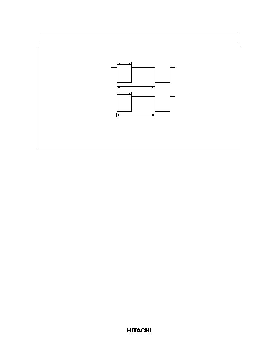
LSB
MSB
1
2
3
4
5
6
7
8
Transmit clock
Serial output
data
Serial input
data latch
timing
Figure 40 Serial Interface Timing

HD404339 Series
53
,
State
MCU reset
PMRA write
SMR write
PMRC write
SCK
pin
STS wait state
Transmit clock
wait state
Transfer state
Transmit clock
wait state
STS wait state
Port selection
External clock selection
Output level control in
idle states
Dummy write for
state transition
Output level control in
idle states
Data write for transmission
Undefined
LSB
MSB
Flag reset at transfer completion
External clock mode
State
MCU reset
PMRA write
SMR write
PMRC write
STS wait state
Transfer state
Transmit clock
wait state
STS wait state
Port selection
Internal clock selection
Output level control in
idle states
Data write for transmission
Output level control in
idle states
Undefined
LSB
MSB
Flag reset at transfer completion
Internal clock mode
(input)
instruction
write
SRL, SRU
STS
SO pin
IFS
SCK
pin
(output)
instruction
write
SRL, SRU
STS
SO pin
IFS
Figure 41 Example of Serial Interface Operation Sequence
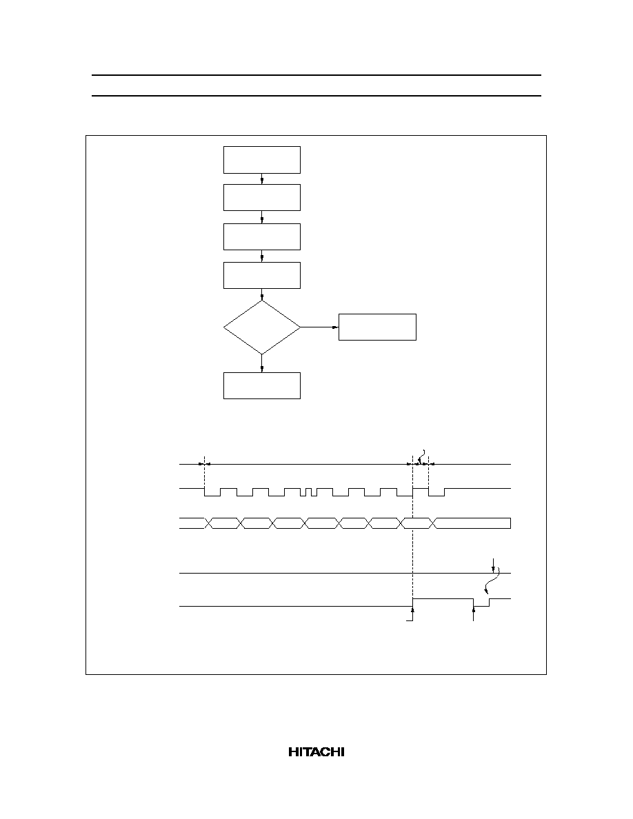
HD404339 Series
54
Transmit clock errors are detected as illustrated in figure 42.
Transfer completion
(IFS 1)
Interrupts inhibited
IFS 0
SMR write
IFS = 1
Transmit clock
error processing
Normal
termination
Yes
No
Transmit clock error detection flowchart
Transmit clock error detection procedure
State
SCK
pin (input)
Transmit clock
wait state
Transfer state
Transfer state
Transmit clock wait state
Noise
Transfer state has been
entered by the transmit
clock error. When SMR
is written, IFS is set.
Flag set because octal
counter reaches 000.
Flag reset at
transfer completion.
SMR write
IFS
1
2
3
4
5
6
7
8
Figure 42 Transmit Clock Error Detection
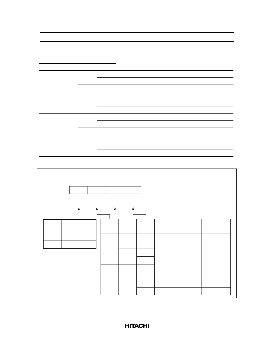
HD404339 Series
55
Table 11
Transmit Clock Selection
PMRC
SMR
Bit 0
Bit 2
Bit 1
Bit 0
System Clock Divisor
Transmit Clock Frequency
0
0
0
0
˜
2048
4096t
cyc
1
˜
512
1024t
cyc
1
0
˜
128
256t
cyc
1
˜
32
64t
cyc
1
0
0
˜
8
16t
cyc
1
˜
2
4t
cyc
1
0
0
0
˜
4096
8192t
cyc
1
˜
1024
2048t
cyc
1
0
˜
256
512t
cyc
1
˜
64
128t
cyc
1
0
0
˜
16
32t
cyc
1
˜
4
8t
cyc
Bit
Initial value
Read/Write
Bit name
3
0
W
SMR3
2
0
W
SMR2
0
0
W
SMR0
1
0
W
SMR1
Serial mode register (SMR: $005)
0
1
0
1
0
1
0
1
0
1
0
1
0
1
SMR2
SMR0
SMR1
SMR3
0
1
R0
0
/
SCK
Mode Selection
R0
0
SCK
SCK
Output
Output
Input
Clock Source
External clock
--
--
Prescaler
Division Ratio
Refer to
table 11
Prescaler
System clock
Figure 43 Serial Mode Register (SMR)
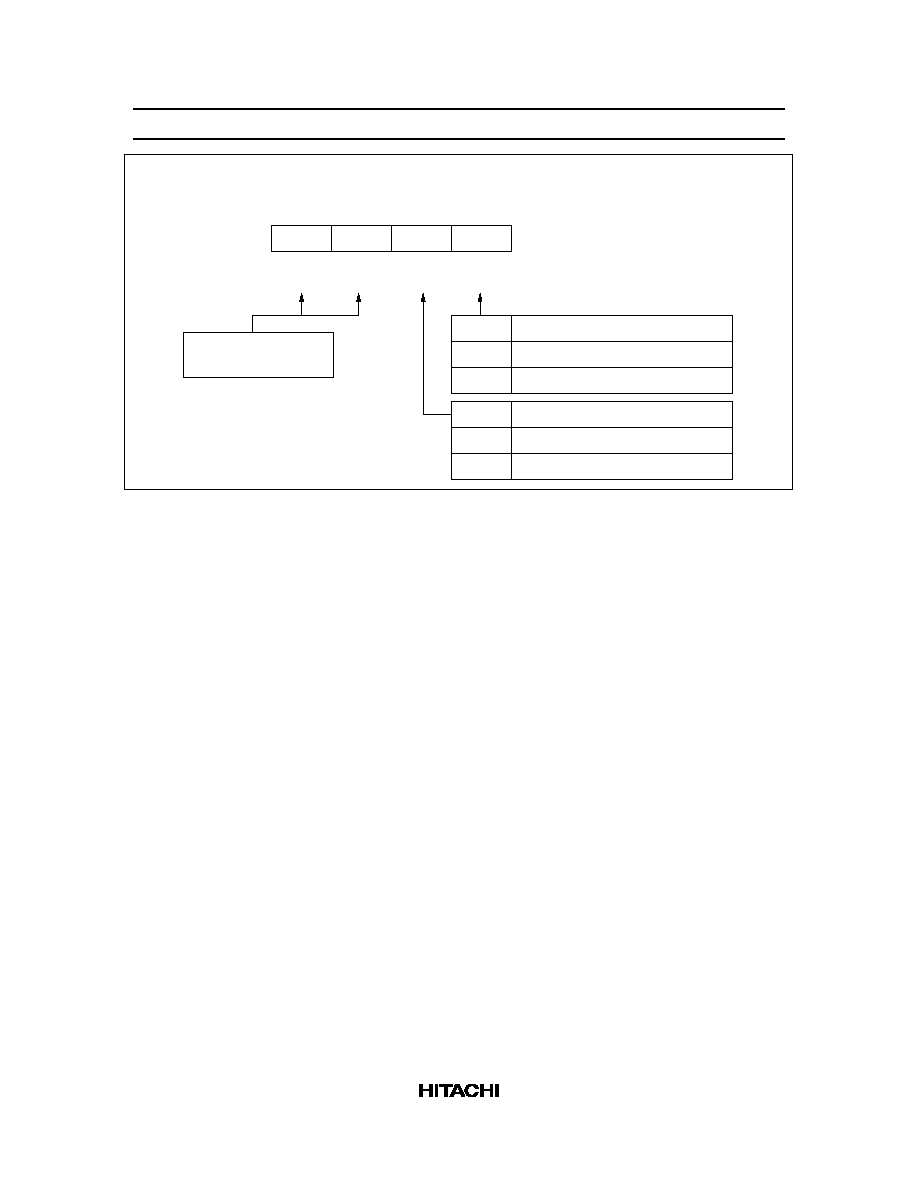
HD404339 Series
56
Bit
Initial value
Read/Write
Bit name
3
0
W
PMRC3
2
0
W
PMRC2
0
0
W
PMRC0
1
Undefined
W
PMRC1
Port mode register C (PMRC: $025)
PMRC1
0
1
Output Level Control in Idle States
Low level
High level
PMRC0
0
1
Serial Clock Division Ratio
Prescaler output divided by 2
Prescaler output divided by 4
Alarm output function.
Refer to table 9.
Figure 44 Port Mode Register C (PMRC)

HD404339 Series
57
A/D Converter
The MCU also contains a built-in A/D converter that uses a sequential comparison method with a
resistance ladder. It can perform digital conversion of twelve analog inputs with 8-bit resolution. The
following describes the A/D converter.
∑
A/D mode register 1 (AMR1: $019) is used to select digital or analog ports
∑
A/D mode register 2 (AMR2: $01A) is used to set the A/D conversion speed and to select digital or
analog ports
∑
The A/D channel register (ACR: $016) is used to select an analog input channel
∑
A/D conversion is started by setting the A/D start flag (ADSF: $020, 2) to 1. After the conversion is
completed, converted data is stored in the A/D data register, and at the same time the A/D start flag is
cleared to 0.
∑
By setting the I
AD
off flag (IAOF: $021, 2) to 1, the current flowing through the resistance ladder can be
cut off even while operating in standby or active mode
∑
The A/D data register is a read-only register consisting of a lower 4 bits and upper 4 bits (ADRL: $017,
ADRU: $018). This register is not cleared by a reset. Data reads during A/D conversion are not
guaranteed. After A/D conversion ends, the resultant 8-bit data is set in this register and held until the
start of the next conversion (figures 51 to 53).

HD404339 Series
58
I
AD
off flag
(IAOF)
Selector
4
A/D channel
register (ACR)
A/D mode
register 2
(AMR2)
A/D mode
register 1
(AMR1)
A/D interrupt
request flag
(IFAD)
Encoder
A/D data
register
(ADRU, L)
A/D start flag
(ADSF)
Operating mode signal (1 in
stop, watch, and subactive modes)
Internal data bus
+
≠
Comp
A/D
controller
AN
0
AN
1
AN
2
AN
3
AN
4
AN
5
AN
6
AN
7
AN
8
AN
9
AN
10
AN
11
Control signal
for conversion
time
4
2
D/A
AV
CC
AV
SS
Figure 45 A/D Converter Block Diagram

HD404339 Series
59
Notes on Usage
∑
Use the SEM or SEMD instruction for writing to the A/D start flag (ADSF)
∑
Do not write to the A/D start flag during A/D conversion
∑
Data in the A/D data register during A/D conversion is undefined
∑
Since the operation of the A/D converter is based on the clock from the system oscillator, the A/D
converter does not operate in stop, watch, or subactive mode. In addition, to save power while in these
modes, all current flowing through the converter's resistance ladder is cut off.
∑
If the power supply for the A/D converter is to be different from V
CC
, connect a 0.1-
µ
F bypass capacitor
between the AV
CC
and AV
SS
pins. (However, this is not necessary when the AV
CC
pin is directly
connected to the V
CC
pin.)
∑
The port data register (PDR) is initialized to 1 by an MCU reset. At this time, if pull-up MOS is selected
as active by bit 3 of the miscellaneous register (MIS3), the port will be pulled up to V
CC
. When using a
shared R port/analog input pin as an input pin, clear PDR to 0. Otherwise, if pull-up MOS is selected by
MIS3 and PDR is set to 1, a pin selected by bit 1 of the A/D mode registr as an analog pin will remain
pulled up.
Bit
Initial value
Read/Write
Bit name
3
0
W
AMR13
2
0
W
AMR12
0
0
W
AMR10
1
0
W
AMR11
AMR10
0
1
AN
0
A/D mode register 1 (AMR1: $019)
AMR11
0
1
AN
1
AMR12
0
1
R3
2
/AN
2
Mode Selection
R3
2
AN
2
AMR13
0
1
R3
3
/AN
3
Mode Selection
R3
3
AN
3
R3
0
/AN
0
Mode Selection
R3
0
R3
1
/AN
1
Mode Selection
R3
1
Figure 46 A/D Mode Register 1 (AMR1)
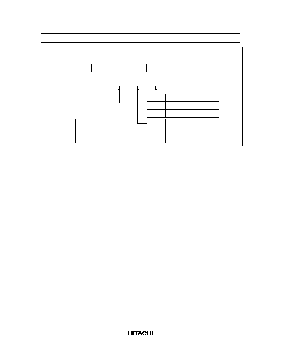
HD404339 Series
60
Bit
Initial value
Read/Write
Bit name
3
--
--
Not used
2
0
W
AMR22
0
0
W
AMR20
1
0
W
AMR21
AMR20
0
1
67 t
cyc
A/D mode register 2 (AMR2: $01A)
AMR21
0
1
AN
4
≠AN
7
AMR22
0
1
R5/AN
8
≠AN
11
Pin Selection
R5
AN
8
≠AN
11
Conversion Time
34 t
cyc
R4/AN
4
≠AN
7
Pin Selection
R4
Figure 47 A/D Mode Register 2 (AMR2)
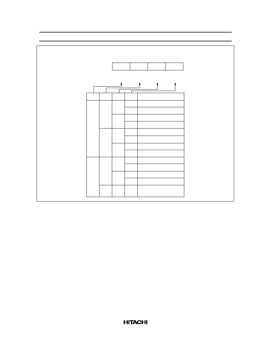
HD404339 Series
61
Bit
Initial value
Read/Write
Bit name
3
0
W
ACR3
2
0
W
ACR2
0
0
W
ACR0
1
0
W
ACR1
A/D channel register (ACR: $016)
0
0
1
0
0
1
0
1
0
1
0
1
0
1
0
1
Don't
care
Analog Input Selection
AN
0
AN
1
AN
2
AN
3
AN
4
AN
5
AN
6
AN
7
AN
8
AN
9
AN
10
AN
11
Not used
ACR3
ACR1
ACR2
ACR0
0
1
1
0
0
1
1
Don't
care
1
Figure 48 A/D Channel Register (ACR)
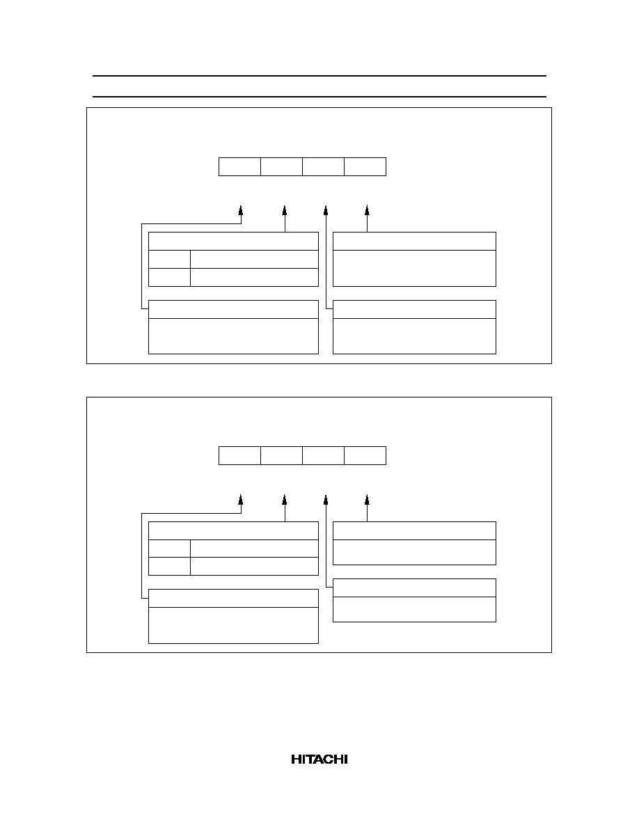
HD404339 Series
62
Bit
Initial value
Read/Write
Bit name
3
0
R/W
DTON
2
0
R/W
ADSF
0
0
R/W
LSON
1
0
W
WDON
A/D start flag (ADSF: $020, bit 2)
Refer to the description of operating
modes
DTON
Refer to the description of timers
WDON
Refer to the description of operating
modes
LSON
0
1
A/D conversion completed
A/D conversion started
A/D Start Flag (ADSF)
Figure 49 A/D Start Flag (ADSF)
Bit
Initial value
Read/Write
Bit name
3
0
R/W
RAME
2
0
R/W
IAOF
0
0
R/W
ICSF
1
0
R/W
ICEF
I
AD
off flag (IAOF: $021, bit 2)
Refer to the description of operating
modes
RAME
Refer to the description of timers
ICEF
Refer to the description of timers
ICSF
0
1
I
AD
current flows
I
AD
current is cut off
I
AD
Off Flag (IAOF)
Figure 50 I
AD
Off Flag (IAOF)

HD404339 Series
63
MSB
bit 7
LSB
bit 0
RESULT
0
1
ADRL: $017
2
3
0
1
ADRU: $018
2
3
Figure 51 A/D Data Register
0
R
0
ADRL0
1
R
0
ADRL1
Bit
Read/write
Initial value after reset
Bit name
A/D data register (lower) (ADRL: $017)
2
R
0
ADRL2
3
R
0
ADRL3
Figure 52 A/D Data Register (Lower) (ADRL)
0
R
0
ADRU0
1
R
0
ADRU1
Bit
Read/write
Initial value after reset
Bit name
A/D data register (upper) (ADRU: $018)
2
R
0
ADRU2
3
R
1
ADRU3
Figure 53 A/D Data Register (Upper) (ADRU)

HD404339 Series
64
Notes on Mounting
Assemble all parts including the HD404339 Series on a board, noting the points described below.
1. Connect layered ceramic type capacitors (about 0.1
µ
F) between AV
CC
and AV
SS
, between V
CC
and
GND, and between used analog pins and AV
SS
.
2. Connect unused analog pins to AV
SS
.
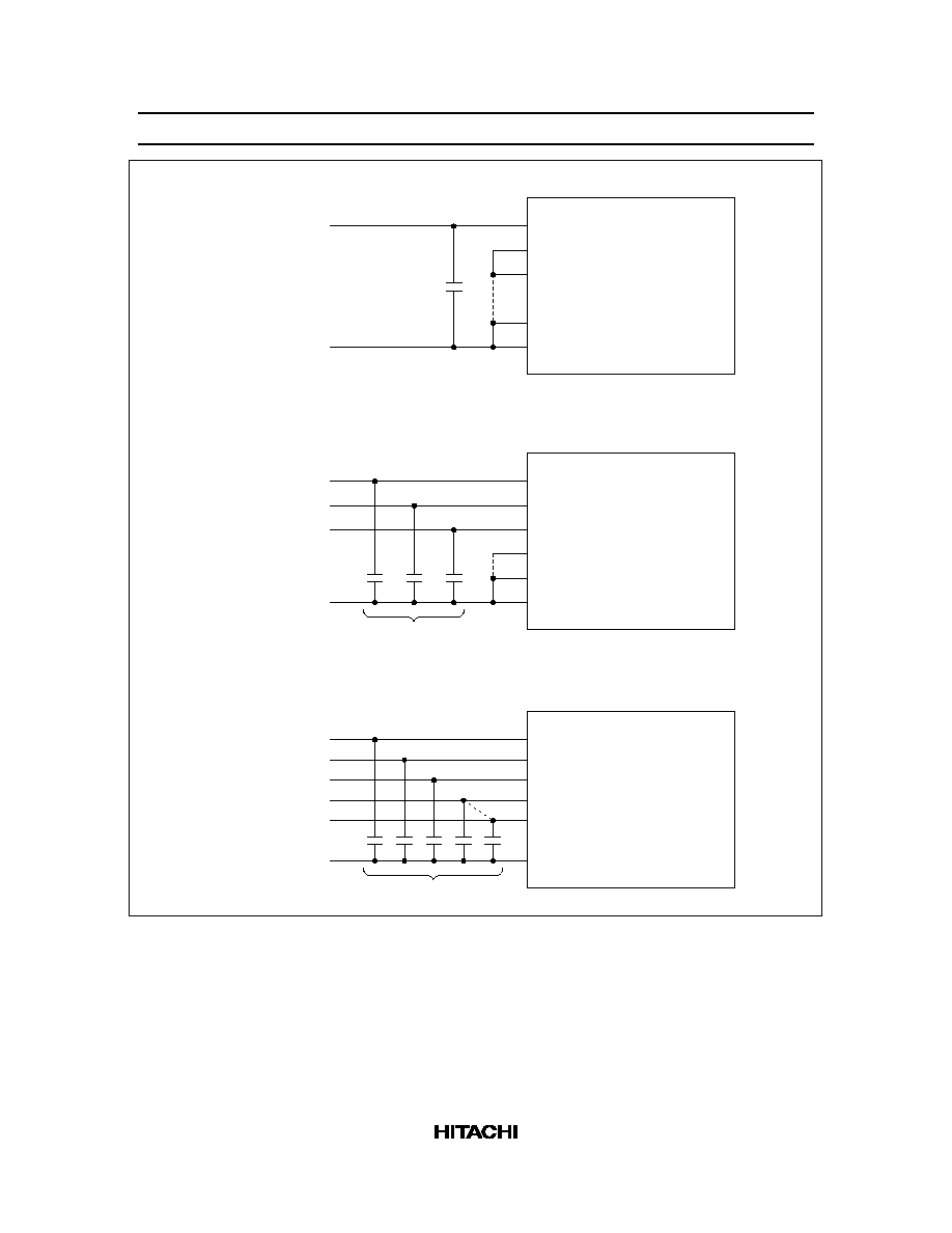
HD404339 Series
65
AV
AN
AN
to
AN
AV
CC
SS
0
1
11
AV
AN
AN
AN to
AN
AV
CC
SS
0
1
2
11
AV
AN
AN
AN to
AN
AV
CC
SS
0
1
2
11
1. When not using an A/D converter.
V
GND
CC
V
GND
CC
V
GND
CC
2. When using pins AN and AN but not using AN to AN .
0
1
2
11
3. When using all analog pins.
0.1
µ
F 3
◊
0.1
µ
F 13
◊
0.1
µ
F
Figure 54 Example of Connections (AV
CC
to AV
SS
)
Between the V
CC
and GND lines, connect capacitors designed for use in ordinary power supply circuits.
An example connection is described in figure 54.
No resistors can be inserted in series in the power supply circuit, so the capacitors should be connected in
parallel. The capacitors are a large capacitance C
1
and a small capacitance C
2
.
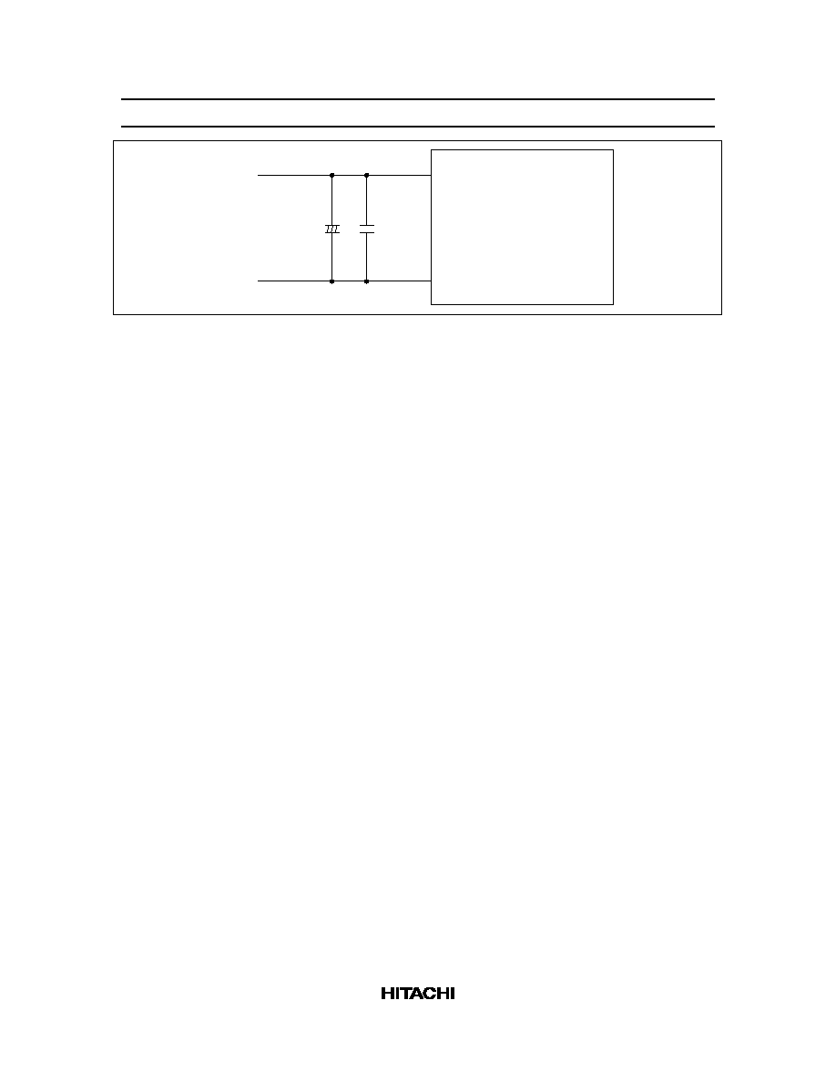
HD404339 Series
66
V
GND
CC
V
GND
CC
C
1
C
2
Figure 55 Example of Connections (V
CC
to GND)
HD404339 Series
67
Absolute Maximum Ratings
Item
Symbol
Value
Unit
Notes
Supply voltage
V
CC
≠0.3 to +7.0
V
Programming voltage
V
PP
≠0.3 to +14.0
V
1
Pin voltage
V
T
≠0.3 to V
CC
+ 0.3
V
2
V
CC
≠ 45 to V
CC
+ 0.3
V
3
Total permissible input current
I
O
70
mA
4
Total permissible output current
≠
I
O
150
mA
5
Maximum input current
I
O
4
mA
6, 7
20
mA
6, 8
Maximum output current
≠I
O
4
mA
9, 10
30
mA
10, 11
Operating temperature
T
opr
≠20 to +75
∞
C
Storage temperature
T
stg
≠55 to +125
∞
C
Notes: Permanent damage may occur if these absolute maximum ratings are exceeded. Normal operation
must be under the conditions stated in the electrical characteristics tables. If these conditions are
exceeded, the LSI may malfunction or its reliability may be affected.
1. Applies to pin TEST (V
PP
) of HD4074339.
2. Applies to all standard voltage pins.
3. Applies to high-voltage pins.
4. The total permissible input current is the total of input currents simultaneously flowing in from all
the I/O pins to GND.
5. The total permissible output current is the total of output currents simultaneously flowing out from
V
CC
to all I/O pins.
6. The maximum input current is the maximum current flowing from each I/O pin to GND.
7. Applies to ports R3, R4, and R5.
8. Applies to ports R0, R6, and R7.
9. Applies to ports R0 and R3 to R7.
10. The maximum output current is the maximum current flowing from V
CC
to each I/O pin.
11. Applies to ports D
0
≠D
13
, R1, R2, R8, and R9.

HD404339 Series
68
Electrical Characteristics
DC Characteristics (V
CC
= 4.0 to 5.5 V, GND = 0 V, V
disp
= V
CC
≠ 40 V to V
C C
, T
a
= ≠20 to +75
∞
C,
unless otherwise specified)
Item
Symbol Pins
Min
Typ
Max
Unit
Test Condition
Notes
Input high voltage
V
IH
RESET
,
SCK
,
SI,
INT
0
,
INT
1
,
STOPC
, EVNB
0.8V
CC
--
V
CC
+ 0.3
V
OSC
1
V
CC
≠ 0.5 --
V
CC
+ 0.3
V
Input low voltage
V
IL
RESET
,
SCK
,
SI
≠0.3
--
0.2V
CC
V
INT
0
,
INT
1
,
STOPC
, EVNB
V
CC
≠ 40 --
0.2V
CC
V
OSC
1
≠0.3
--
0.5
V
Output high
voltage
V
OH
SCK
, SO, TOC V
CC
≠ 0.5 --
--
V
≠I
OH
= 0.5 mA
Output low voltage V
OL
SCK
, SO, TOC --
--
0.4
V
I
OL
= 0.4 mA
I/O leakage
current
|I
IL
|
RESET
,
SCK
,
SI, SO,TOC,
OSC
1
--
--
1
µ
A
V
in
= 0 V to V
CC
1
INT
0
,
INT
1
,
STOPC
, EVNB
--
--
20
µ
A
V
in
= V
CC
≠ 40 to
V
CC
1
Current dissipation
in active mode
I
CC
V
CC
--
--
5.0
mA
V
CC
= 5 V,
f
OSC
= 4 MHz
2, 5
--
--
8.0
mA
2, 6
Current dissipation
in standby mode
I
SBY
V
CC
--
--
2.0
mA
V
CC
= 5 V,
f
OSC
= 4 MHz
3
Current dissipation
in subactive mode
I
SUB
V
CC
--
--
100
µ
A
V
CC
= 5 V,
32 kHz oscillator
4, 5
--
--
320
µ
A
4, 6
Current dissipation
in watch mode
I
WTC
V
CC
--
--
20
µ
A
V
CC
= 5 V,
32 kHz oscillator
4
Current dissipation
in stop mode
I
STOP
V
CC
--
--
10
µ
A
X1 = GND,
X2 = Open
4, 5
--
--
20
µ
A
4, 6
Stop mode
retaining voltage
V
STOP
V
CC
2
--
--
V

HD404339 Series
69
Notes: 1. Excludes current flowing through pull-up MOS and output buffers.
2. I
CC
is the source current when no I/O current is flowing while the MCU is in reset state.
Test conditions:
MCU:
Reset
Pins:
RESET
, TEST at GND
R0, R3
0
to R7
2
at V
CC
D
0
≠D
13
, R1, R2, R8, R9, RA
1
at V
disp
3. I
SBY
is the source current when no I/O current is flowing while the MCU timer is operating.
Test conditions:
MCU:
I/O reset
Standby mode
Pins:
RESET
at V
CC
TEST at GND
R0, R3
0
to R7
2
at V
CC
D
0
≠D
13
, R1, R2, R8, R9, RA
1
at V
disp
4. This is the source current when no I/O current is flowing.
Test conditions: Pins: R0, R3
0
to R7
2
at V
CC
D
0
≠D
13
, R1, R2, R8, R9, RA
1
at GND
5. Applies to the HD404334, HD404336, HD404338, HD4043312, and HD404339.
6. Applies to the HD4074339.

HD404339 Series
70
I/O Characteristics for High-Voltage Pins (V
CC
= 4.0 to 5.5 V, GND = 0 V, V
disp
= V
CC
≠ 40 V to V
CC
,
T
a
= ≠20 to +75
∞
C, unless otherwise specified)
Item
Symbol
Pins
Min
Typ Max
Unit Test Condition
Note
Input high voltage
V
IH
D
0
≠D
13
, R1,
R2, R8, R9,
RA
1
0.7V
CC
--
V
CC
+ 0.3 V
Input low voltage
V
IL
D
0
≠D
13
, R1,
R2, R8, R9,
RA
1
V
CC
≠ 40
--
0.3V
CC
V
Output high
voltage
V
OH
D
0
≠D
13
, R1,
R2, R8, R9,
BUZZ
V
CC
≠ 3.0 --
--
V
≠I
OH
= 15 mA
V
CC
≠ 2.0 --
--
V
≠I
OH
= 10 mA
V
CC
≠ 1.0 --
--
V
≠I
OH
= 4 mA
Output low voltage V
OL
D
0
≠D
13
, R1,
R2, R8, R9,
BUZZ
--
--
V
CC
≠ 37
V
V
disp
= V
CC
≠ 40 V
1
--
--
V
CC
≠ 37
V
150 k
at V
CC
≠ 40 V
2
I/O leakage
current
|I
IL
|
D
0
≠D
13
, R1,
R2, R8, R9,
RA
1
, BUZZ
--
--
20
µ
A
V
in
= V
CC
≠ 40 V to V
CC
3
Pull-down MOS
current
I
PD
D
0
≠D
13
, R1,
R2, R8, R9
200
600 1000
µ
A
V
disp
= V
CC
≠ 35 V,
V
in
= V
CC
1
Notes: 1. Applies to pins with pull-down MOS as selected by the mask option .
2. Applies to pins without pull-down MOS as selected by the mask option.
3. Excludes output buffer current.
HD404339 Series
71
A/D Converter Characteristics (V
CC
= 4.0 to 5.5 V, GND = 0 V, V
disp
= V
CC
≠ 40 V to V
CC
, T
a
= ≠20 to
+75
∞
C, unless otherwise specified)
Item
Symbol
Pins
Min
Typ
Max
Unit
Test Condition
Note
Analog supply
voltage
AV
CC
AV
CC
V
CC
≠ 0.3 V
CC
V
CC
+ 0.3
V
1
Analog input
voltage
AV
in
AN
0
≠AN
11
AV
SS
--
AV
CC
V
Current flowing
between AV
CC
and
AV
SS
I
AD
--
--
200
µ
A
V
CC
= AV
CC
= 5.0 V
Analog input
capacitance
CA
in
AN
0
≠AN
11
--
--
30
pF
Resolution
8
8
8
Bit
Number of input
channels
0
--
12
Channel
Absolute accuracy
--
--
±
2.0
LSB
Conversion time
34
--
67
t
cyc
Input impedance
AN
0
≠AN
11
1
--
--
M
Note: 1. Connect this to V
CC
if the A/D converter is not used.

HD404339 Series
72
AC Characteristics (V
CC
= 4.0 to 5.5 V, GND = 0 V, V
disp
= V
CC
≠ 40 V to V
CC
, T
a
= ≠20 to +75
∞
C)
Item
Symbol Pins
Min
Typ
Max
Unit
Test Condition
Note
Clock oscillation frequency
f
OSC
OSC
1
,
OSC
2
0.4
4
4.5
MHz
System clock
divided by 4
1
X1, X2
--
32.768
--
kHz
Instruction cycle time
t
cyc
0.89
1
10
µ
s
1
t
subcyc
--
244.14
--
µ
s
32-kHz oscillator,
1/8 system clock
division ratio
--
122.07
--
µ
s
32-kHz oscillator,
1/4 system clock
division ratio
Oscillation stabilization time
(ceramic oscillator)
t
RC
OSC
1
,
OSC
2
--
--
7.5
ms
2
Oscillation stabilization time
(crystal oscillator)
t
RC
OSC
1
,
OSC
2
--
--
40
ms
2
X1, X2
--
--
2
s
2
External clock high width
t
CPH
OSC
1
92
--
--
ns
3
External clock low width
t
CPL
OSC
1
92
--
--
ns
3
External clock rise time
t
CPr
OSC
1
--
--
20
ns
3
External clock fall time
t
CPf
OSC
1
--
--
20
ns
3
INT
0
,
INT
1
, EVNB high
widths
t
IH
INT
0
,
INT
1
,
EVNB
2
--
--
t
cyc
/
t
subcyc
4
INT
0
,
INT
1
, EVNB low widths t
IL
INT
0
,
INT
1
,
EVNB
2
--
--
t
cyc
/
t
subcyc
4
RESET
low width
t
RSTL
RESET
2
--
--
t
cyc
5
STOPC
low width
t
STPL
STOPC
1
--
--
t
RC
6
RESET
rise time
t
RSTr
RESET
--
--
20
ms
5
STOPC
rise time
t
STPr
STOPC
--
--
20
ms
6
Input capacitance
C
in
All input
pins except
TEST
--
--
30
pF
f = 1 MHz,
V
in
= 0 V
TEST
--
--
30
pF
f = 1 MHz,
V
in
= 0 V
7
--
--
180
pF
8
Notes: 1. When using the subsystem oscillator (32.768 kHz), one of the following relationships for f
OSC
must be applied.
0.4 MHz
f
OSC
1.0 MHz or 1.6 MHz
f
OSC
4.5 MHz
The operating range for f
OSC
can be set with bit 1 of system selection register 1 (SSR1: $027).
2. The oscillation stabilization time is the period required for the oscillator to stabilize in the
following situations:

HD404339 Series
73
a. After V
CC
reaches 4.0 V at power-on.
b. After
RESET
input goes low when stop mode is cancelled.
c. After
STOPC
input goes low when stop mode is cancelled.
To ensure the oscillation stabilization time at power-on or when stop mode is cancelled,
RESET
or
STOPC
must be input for at least a duration of t
RC
.
When using a crystal or ceramic oscillator, consult with the manufacturer to determine what
stabilization time is required, since it will depend on the circuit constants and stray capacitance.
3. Refer to figure 56.
4. Refer to figure 57.
5. Refer to figure 58.
6. Refer to figure 59.
7. Applies to the HD404334, HD404336, HD404338, HD4043312, and HD404339.
8. Applies to the HD4074339.
Serial Interface Timing Characteristics (V
CC
= 4.0 to 5.5 V, GND = 0 V, V
disp
= V
CC
≠ 40 V to V
CC
, T
a
=
≠20 to +75
∞
C, unless otherwise specified)
During Transmit Clock Output
Item
Symbol Pins
Min
Typ Max Unit Test Condition
Note
Transmit clock cycle time
t
Scyc
SCK
1
--
--
t
cyc
Load shown in figure 61
1
Transmit clock high width
t
SCKH
SCK
0.4
--
--
t
Scyc
Load shown in figure 61
1
Transmit clock low width
t
SCKL
SCK
0.4
--
--
t
Scyc
Load shown in figure 61
1
Transmit clock rise time
t
SCKr
SCK
--
--
80
ns
Load shown in figure 61
1
Transmit clock fall time
t
SCKf
SCK
--
--
80
ns
Load shown in figure 61
1
Serial output data delay time
t
DSO
SO
--
--
300
ns
Load shown in figure 61
1
Serial input data setup time
t
SSI
SI
100
--
--
ns
1
Serial input data hold time
t
HSI
SI
200
--
--
ns
1
During Transmit Clock Input
Item
Symbol
Pins
Min
Typ Max Unit Test Condition
Note
Transmit clock cycle time
t
Scyc
SCK
1
--
--
t
cyc
1
Transmit clock high width
t
SCKH
SCK
0.4
--
--
t
Scyc
1
Transmit clock low width
t
SCKL
SCK
0.4
--
--
t
Scyc
1
Transmit clock rise time
t
SCKr
SCK
--
--
80
ns
1
Transmit clock fall time
t
SCKf
SCK
--
--
80
ns
1
Serial output data delay time t
DSO
SO
--
--
300
ns
Load shown in figure 61
1
Serial input data setup time
t
SSI
SI
100
--
--
ns
1
Serial input data hold time
t
HSI
SI
200
--
--
ns
1
Note:
1. Refer to figure 60.
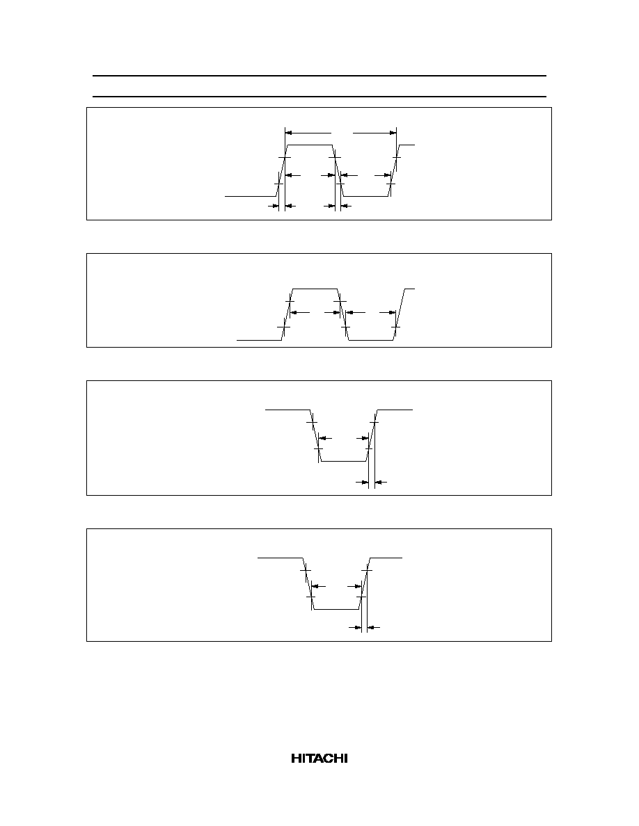
HD404339 Series
74
t
CPr
t
CPf
V
CC
≠ 0.5 V
0.5 V
OSC
1
t
CPH
t
CPL
1/f
CP
Figure 56 External Clock Timing
0.8V
CC
0.2V
CC
INT
0
,
INT
1
, EVNB
t
IH
t
IL
Figure 57 Interrupt Timing
RESET
t
RSTr
t
RSTL
0.2V
CC
0.8V
CC
Figure 58
RESET Timing
t
STPr
t
STPL
0.8V
CC
0.2V
CC
STOPC
Figure 59
STOPC Timing
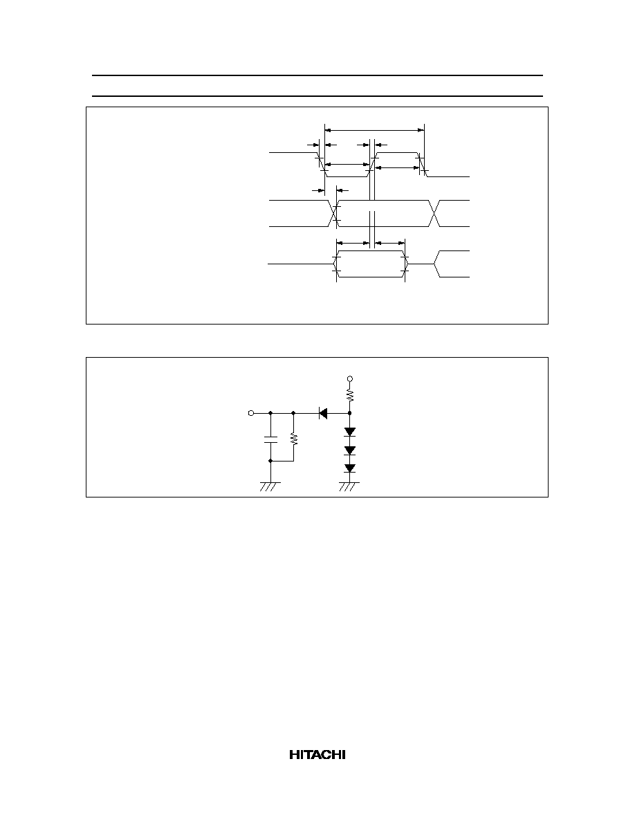
HD404339 Series
75
0.8V
CC
0.2V
CC
t
DSO
t
SCKf
t
SCKL
t
SSI
t
HSI
t
Scyc
t
SCKr
0.8 V
V ≠ 2.0 V
CC
V ≠ 2.0 V (0.8V )
*
CC
0.8 V (0.2V )
*
SCK
SO
SI
Note:
*
V
CC
≠ 2.0 V and 0.8 V are the threshold voltages for transmit clock output, and
0.8V
CC
and 0.2V
CC
are the threshold voltages for transmit clock input.
CC
CC
t
SCKH
Figure 60 Serial Interface Timing
R
L
= 2.6 k
V
CC
Hitachi
1S2074
or equivalent
R =
12 k
Test
point
C =
30 pF
Figure 61 Timing Load Circuit
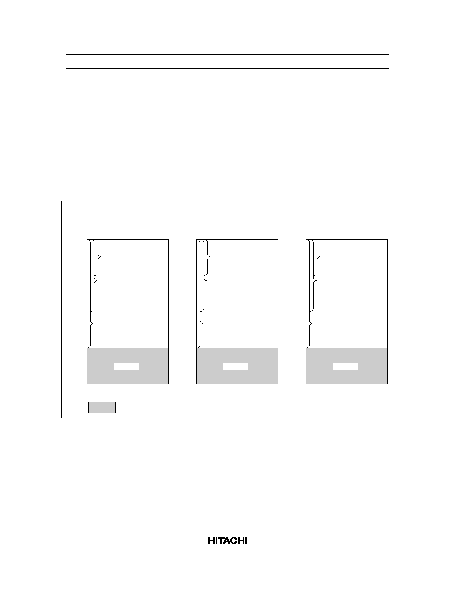
HD404339 Series
76
Notes on ROM Out
Please pay attention to the following items regarding ROM out.
On ROM out, fill the ROM area indicated below with 1s to create the same data size for the HD404334 and
HD404336 as an 8-kword version (HD404338), and to create the same data size for t he HD4043312 as a
16-kword version (HD404339).
The 8-kword and 16-kword data sizes are required to change ROM data to mask manufacturing data since
the program used is for an 8-k or 16-kword version.
This limitation applies when using an EPROM or a data base.
Vector address
Zero-page subroutine
(64 words)
Pattern & program
(4,096 words)
Not used
Vector address
Zero-page subroutine
(64 words)
Pattern & program
(6,144 words)
Not used
ROM 4-kword version:
HD404334
Address $1000≠$1FFF
ROM 6-kword version:
HD404336
Address $1800≠$1FFF
$0000
$000F
$0010
$003F
$0040
$0FFF
$1000
$1FFF
$0000
$000F
$0010
$003F
$0040
$17FF
$1800
$1FFF
Fill this area with 1s
Vector address
Zero-page subroutine
(64 words)
Pattern & program
(12,288 words)
Not used
ROM 12-kword version:
HD4043312
Address $3000≠$3FFF
$0000
$000F
$0010
$003F
$0040
$2FFF
$3000
$3FFF
HD404339 Series
77
HD404334/HD404336/HD404338/HD4043312/HD404339 Option List
5. ROM Code Media
EPROM:
Ceramic oscillator
Crystal oscillator
External clock
f = MHz
f = MHz
f = MHz
6. System Oscillator (OSC1, OSC2)
RA1 without pull-down resistance
Vdisp
4. RA1/Vdisp
Note: If even only one pin is selected with I/O option E, pin RA1/Vdisp must be selected to function as Vdisp.
With 32-kHz CPU operation, with time base for clock
Without 32-kHz CPU operation, with time base for clock
Without 32-kHz CPU operation, without time base
*
*
2. Optional Functions
3. I/O Options
Note:
*
Options marked with an asterisk require a subsystem crystal oscillator (X1, X2).
The upper bits and lower bits are mixed together. The upper five bits and lower five bits
are programmed to the same EPROM in alternating order (i.e., LULULU...).
EPROM: The upper bits and lower bits are separated. The upper five bits and lower five bits are
programmed to different EPROMS.
FP-64B
DP-64S
8. Package
Please specify the first type below (the upper bits and lower bits are mixed together), when using the
EPROM on-package microcomputer type (including ZTATTM version).
Used
Not used
7. Stop Mode
Date of order
Customer
Department
Name
ROM code name
LSI number
HD404334
HD404336
HD404338
HD4043312
HD404339
1. ROM Size
4-kword
6-kword
8-kword
12-kword
16-kword
D0/
INT
0
D1/
INT
1
D2/EVNB
D3/BUZZ
D4/
STOPC
D5
D6
D7
D8
D9
D10
D11
D12
D13
Pin name
I/O
I/O
I/O
I/O
I/O
I/O
I/O
I/O
I/O
I/O
I/O
I/O
I/O
I/O
I/O
I/O option
D
E
D: Without pull-down resistance
R1
R2
R8
R9
R10
R11
R12
R13
R20
R21
R22
R23
R80
R81
R82
R83
R90
R91
R92
R93
Pin name
I/O
I/O
I/O
I/O
I/O
I/O
I/O
I/O
I/O
I/O
I/O
I/O
I/O
I/O
I/O
I/O
I/O
I/O option
D
E
E: With pull-down resistance
Please check off the appropriate applications and enter
the necessary information.

HD404339 Series
78
Cautions
1. Hitachi neither warrants nor grants licenses of any rights of Hitachi's or any third party's patent,
copyright, trademark, or other intellectual property rights for information contained in this document.
Hitachi bears no responsibility for problems that may arise with third party's rights, including
intellectual property rights, in connection with use of the information contained in this document.
2. Products and product specifications may be subject to change without notice. Confirm that you have
received the latest product standards or specifications before final design, purchase or use.
3. Hitachi makes every attempt to ensure that its products are of high quality and reliability. However,
contact Hitachi's sales office before using the product in an application that demands especially high
quality and reliability or where its failure or malfunction may directly threaten human life or cause risk
of bodily injury, such as aerospace, aeronautics, nuclear power, combustion control, transportation,
traffic, safety equipment or medical equipment for life support.
4. Design your application so that the product is used within the ranges guaranteed by Hitachi particularly
for maximum rating, operating supply voltage range, heat radiation characteristics, installation
conditions and other characteristics. Hitachi bears no responsibility for failure or damage when used
beyond the guaranteed ranges. Even within the guaranteed ranges, consider normally foreseeable
failure rates or failure modes in semiconductor devices and employ systemic measures such as fail-
safes, so that the equipment incorporating Hitachi product does not cause bodily injury, fire or other
consequential damage due to operation of the Hitachi product.
5. This product is not designed to be radiation resistant.
6. No one is permitted to reproduce or duplicate, in any form, the whole or part of this document without
written approval from Hitachi.
7. Contact Hitachi's sales office for any questions regarding this document or Hitachi semiconductor
products.
Hitachi, Ltd.
Semiconductor & Integrated Circuits.
Nippon Bldg., 2-6-2, Ohte-machi, Chiyoda-ku, Tokyo 100-0004, Japan
Tel: Tokyo (03) 3270-2111 Fax: (03) 3270-5109
Copyright © Hitachi, Ltd., 1998. All rights reserved. Printed in Japan.
Hitachi Asia Pte. Ltd.
16 Collyer Quay #20-00
Hitachi Tower
Singapore 049318
Tel: 535-2100
Fax: 535-1533
URL
NorthAmerica
: http:semiconductor.hitachi.com/
Europe
: http://www.hitachi-eu.com/hel/ecg
Asia (Singapore)
: http://www.has.hitachi.com.sg/grp3/sicd/index.htm
Asia (Taiwan)
: http://www.hitachi.com.tw/E/Product/SICD_Frame.htm
Asia (HongKong)
: http://www.hitachi.com.hk/eng/bo/grp3/index.htm
Japan
: http://www.hitachi.co.jp/Sicd/indx.htm
Hitachi Asia Ltd.
Taipei Branch Office
3F, Hung Kuo Building. No.167,
Tun-Hwa North Road, Taipei (105)
Tel: <886> (2) 2718-3666
Fax: <886> (2) 2718-8180
Hitachi Asia (Hong Kong) Ltd.
Group III (Electronic Components)
7/F., North Tower, World Finance Centre,
Harbour City, Canton Road, Tsim Sha Tsui,
Kowloon, Hong Kong
Tel: <852> (2) 735 9218
Fax: <852> (2) 730 0281
Telex: 40815 HITEC HX
Hitachi Europe Ltd.
Electronic Components Group.
Whitebrook Park
Lower Cookham Road
Maidenhead
Berkshire SL6 8YA, United Kingdom
Tel: <44> (1628) 585000
Fax: <44> (1628) 778322
Hitachi Europe GmbH
Electronic components Group
Dornacher Straþe 3
D-85622 Feldkirchen, Munich
Germany
Tel: <49> (89) 9 9180-0
Fax: <49> (89) 9 29 30 00
Hitachi Semiconductor
(America) Inc.
179 East Tasman Drive,
San Jose,CA 95134
Tel: <1> (408) 433-1990
Fax: <1>(408) 433-0223
For further information write to: