 | –≠–ª–µ–∫—Ç—Ä–æ–Ω–Ω—ã–π –∫–æ–º–ø–æ–Ω–µ–Ω—Ç: HD404448H | –°–∫–∞—á–∞—Ç—å:  PDF PDF  ZIP ZIP |
HD404449 Series
Rev. 6.0
Sept. 1998
Description
The HD404449 Series is a HMCS400-series microcomputer designed to increase program productivity
with large-capacity memory. Each microcomputer has four timers, two serial interfaces, A/D converter,
input capture circuit, 32-kHz oscillator for clock, and four low-power dissipation modes.
The HD404449 Series includes three chips: the HD404448 with 8-kword ROM; the HD404449 with 16-
kword ROM; and HD4074449 with 16-kword PROM (ZTAT
TM
version).
The HD4074449 is a PROM version (ZTAT
TM
microcomputer). A program can be written to the PROM by
a PROM writer, which can dramatically shorten system development periods and smooth the process from
debugging to mass production. (The ZTAT
TM
version is 27256-compatible.)
ZTAT
TM
: Zero Turn Around Time ZTAT is a trademark of Hitachi Ltd.
Features
∑
8,192-word
◊
10-bit ROM (HD404448)
16,384-word
◊
10-bit ROM (HD404449 and HD4074449)
∑
1,152-digit
◊
4-bit RAM
∑
64 I/O pins, including 10 high-current pins (15 mA, max)
∑
Four timer/counters
∑
Eight-bit input capture circuit
∑
Three timer outputs (including two PWM outputs)
∑
Two event counter inputs (including one double-edge function)
∑
Two clock-synchronous 8-bit serial interfaces
∑
A/D converter (4-channel
◊
8-bit)
∑
Built-in oscillators
Main clock: 4-MHz ceramic oscillator or crystal (an external clock is also possible)
Subclock: 32.768-kHz crystal
∑
Eleven interrupt sources
Four by external sources, including two double-edge function
Seven by internal sources

HD404449 Series
2
∑
Subroutine stack up to 16 levels, including interrupts
∑
Four low-power dissipation modes
Subactive mode
Standby mode
Watch mode
Stop mode
∑
One external input for transition from stop mode to active mode
∑
Instruction cycle time: 1
µ
s (f
OSC
= 4 MHz)
∑
Two operating modes
MCU mode (HD404448, HD404449)
MCU/PROM mode (HD4074449)
Ordering Information
Type
Product Name
Model Name
ROM (Words)
Package
Mask ROM
HD404448
HD404448H
8,192
80-pin plastic QFP (FP-80A)
HD404448TF
80-pin plastic QFP (TFP-80F)
HD404449
HD404449H
16,384
80-pin plastic QFP (FP-80A)
HD404449TF
80-pin plastic QFP (TFP-80F)
ZTAT
TM
HD4074449
HD4074449H
16,384
80-pin plastic QFP (FP-80A)
HD4074449TF
80-pin plastic QFP (TFP-80F)
HD404449 Series
3
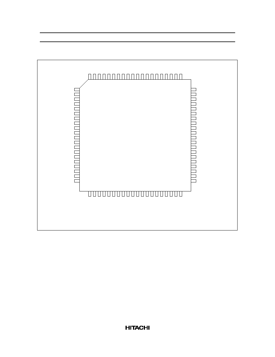
Pin Arrangement
FP-80A
TFP-80F
1
2
3
4
5
6
7
8
9
10
11
12
13
14
15
16
17
18
19
20
60
59
58
57
56
55
54
53
52
51
50
49
48
47
46
45
44
43
42
41
(Top view)
21
22
23
24
25
26
27
28
29
30
31
32
33
34
35
36
37
38
39
40
80
79
78
77
76
75
74
73
72
71
70
69
68
67
66
65
64
63
62
61
R8
3
R8
2
R8
1
R8
0
R7
3
R7
2
R7
1
R7
0
R6
3
R6
2
R6
1
R6
0
R5
3
/SO
2
R5
2
/SI
2
R5
1
/
SCK
2
R5
0
R4
3
/SO
1
R4
2
/SI
1
R4
1
/
SCK
1
R4
0
/EVND
AN
2
AN
3
AV
SS
TEST
OSC
1
OSC
2
RESET
X1
X2
GND
D
0
D
1
D
2
D
3
D
4
D
5
D
6
D
7
D
8
D
9
D
10
D
11
D
12
/
STOPC
D
13
/
INT
0
0
/
INT
1
R0
1
/INT
2
R0
2
/INT
3
R0
3
R1
0
R1
1
R1
2
R1
3
R2
0
R2
1
R2
2
R2
3
R3
0
/TOB
R3
1
/TOC
R3
2
/TOD
R3
3
/
EVNB
AN
1
AN
0
AV
CC
V
CC
RC
3
RC
2
RC
1
RC
0
RB
3
RB
2
RB
1
RB
0
RA
3
RA
2
RA
1
RA
0
R9
3
R9
2
R9
1
R9
0
R0

HD404449 Series
4
Pin Description
Item
Symbol
Pin Number I/O
Function
Power supply
V
CC
77
Applies power voltage
GND
10
Connected to ground
Test
TEST
4
I
Used for factory testing only: Connect this pin to V
CC
Reset
RESET
7
I
Resets the MCU
Oscillator
OSC
1
5
I
Input/output pins for the internal oscillator circuit:
Connect them to a ceramic oscillator, crystal, or
connect OSC
1
to an external oscillator circuit
OSC
2
6
O
X1
8
I
Used for a 32.768-kHz crystal for clock purposes. If
not to be used, fix the X1 pin to V
CC
and leave the X2
pin open.
X2
9
O
Port
D
0
≠D
11
11≠22
I/O
Input/output pins addressed by individual bits; pins
D
0
≠D
9
are high-current pins that can each supply up to
15 mA
D
12
, D
13
23, 24
I
Input pins addressable by individual bits
R0
0
≠RC
3
25≠76
I/O
Input/output pins addressable in 4-bit units
Interrupt
INT
0
,
INT
1
,
INT
2
, INT
3
24≠27
I
Input pins for external interrupts
Stop clear
STOPC
23
I
Input pin for transition from stop mode to active mode
Serial
SCK
1
,
SCK
2
42, 46
I/O
Serial clock input/output pin
interface
SI
1
, SI
2
43, 47
I
Serial receive data input pin
SO
1
, SO
2
44, 48
O
Serial transmit data output pin
Timer
TOB, TOC, TOD 37≠39
O
Timer output pins
EVNB
, EVND
40, 41
I
Event count input pins
A/D converter
AV
CC
78
Power pin for A/D converter: Connect it to the same
potential as V
CC
, as physically close to the V
CC
pin as
possible
AV
SS
3
Ground for AV
CC
: Connect it to the same potential as
GND, as physically close to the GND pin as possible
AN
0
≠AN
3
79, 80, 1, 2
I
Analog input pins for A/D converter

HD404449 Series
5
Block Diagram
System control
External
interrupt
Timer
A
Timer
B
Timer
C
Timer
D
Serial
interface
1
Serial
interface
2
A/D
converter
Internal data bus
Internal address bus
RAM
(1,152 4 bits)
W
(2 bits)
X
(4 bits)
Y
(4 bits)
SPX
(4 bits)
ST
(1 bit)
CA
(1 bit)
A
(4 bits)
B
(4 bits)
SP
(10 bits)
PC
(14 bits)
Instruction
decoder
CPU
R0
R0
R0
R0
R1
R1
R1
R1
R2
R2
R2
R2
R3
R3
R3
R3
R4
R4
R4
R4
R5
R5
R5
R5
R6
R6
R6
R6
R7
R7
R7
R7
R8
R8
R8
R8
R9
R9
R9
R9
RA
RA
RA
RA
RB
RB
RB
RB
RC
RC
RC
RC
: Data bus
: Signal line
RESET
TOC
EVND
TOD
INT
INT
INT
INT
SI
2
SO
2
SCK
2
AV
CC
AV
SS
AN
0
AN
1
AN
2
AN
3
R0 port
R1 port
R2 port
R3 port
R4 port
RC port
0
1
2
3
0
1
2
3
0
1
2
3
0
1
2
3
0
1
2
3
0
1
2
3
0
1
2
3
0
1
2
3
0
1
2
3
0
1
2
3
0
1
2
3
0
1
2
3
0
1
2
3
R5 port
R6 port
R7 port
R8 port
R9 port
RA port
RB port
SI
SO
SCK
ROM
(16,384
◊
10 bits)
(8,192
◊
10 bits)
D port
High current
pins
D
D
D
D
D
D
D
D
D
D
D
D
D
D
0
1
2
3
4
5
6
7
8
9
10
11
12
13
0
1
2
3
EVNB
TOB
1
1
1
SPY
(4 bits)
ALU
◊
TEST
STOPC
OSC
1
OSC
2
X1
X2
V
CC
GND