HD404654 Series
4-Bit Single-Chip Microcomputer
Rev. 7.0
Sept. 1999
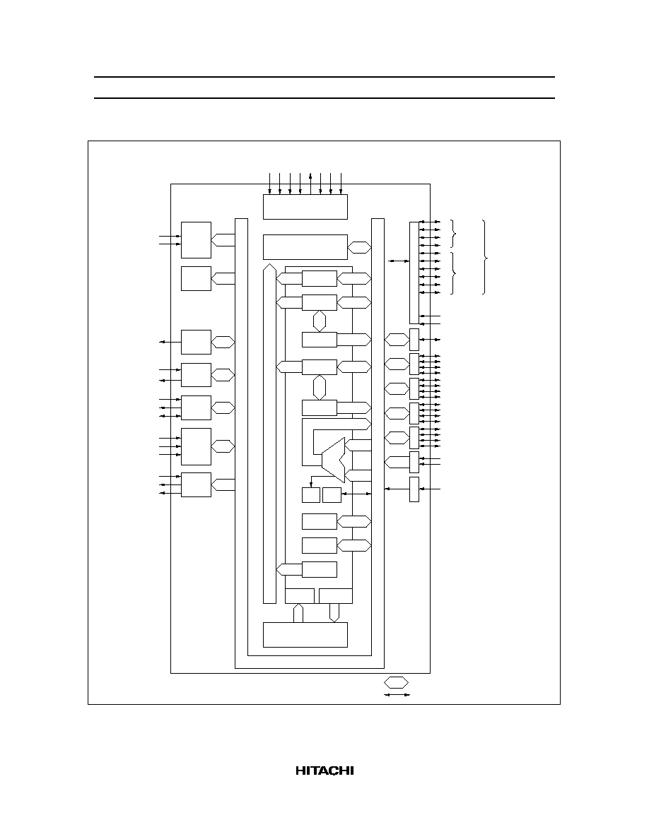
Description
The HD404654 Series is a member of the HMCS400-series of microcomputers designed to increase
program productivity with large-capacity memory. Each microcomputer has a high-precision dual-tone
multi-frequency (DTMF) generator, three timers, serial interface, voltage comparator, and input capture
circuit.
The HD404654 Series includes three chips: the HD404652 with 2 k-word ROM; the HD404654 with 4 k-
word ROM; and the HD4074654 with 4 k-word PROM (ZTAT
TM
version).
The HD4074654 is a PROM version (ZTAT
TM
microcomputer). A program can be written to the PROM by
a PROM writer, which can dramatically shorten system development periods and smooth the process from
debugging to mass production. (The ZTAT
TM
version is 27256-compatible.)
ZTAT
TM
: Zero Turn Around Time. ZTAT is a trademark of Hitachi Ltd.
Features
�
27 I/O pins and 5 dedicated input pins
10 high-current output pins: Six 15-mA sinks and four 10-mA sources
�
Three timer/counters
�
Eight-bit input capture circuit
�
Two timer outputs (including two PWM outputs)
�
One event counter input (including one double-edge function)
�
One clock-synchronous 8-bit serial interface
�
Voltage comparator (2 channels)
�
On-chip DTMF generator (f
OSC
= 400 kHz, 800 kHz, 2 MHz, 3.58 MHz or 4 MHz)
�
Built-in oscillators
Main clock: Ceramic or crystal oscillator (an external clock is also possible)
�
Six interrupt sources
Two by external sources
Four by internal sources
�
Subroutine stack up to 16 levels, including interrupts
HD404654 Series
2
�
Two low-power dissipation modes
Standby mode
Stop mode
�
One external input for transition from stop mode to active mode
�
Instruction cycle time: 1
�
s (f
OSC
= 4 MHz at 1/4 division ratio)
1/4 or 1/32 division ratio can be selected by hardware
�
Two operating modes
MCU mode
MCU/PROM mode (HD4074654)
Ordering Information
Type
Product Name
Model Name
ROM (Words)
RAM (digit)
Package
Mask ROM HD404652
HD404652H
2,048
512
FP-44A
HD404652S
DP-42S
HD404654
HD404654H
4,096
FP-44A
HD404654S
DP-42S
ZTAT
TM
HD4074654
HD4074654H
4,096
FP-44A
HD4074654S
DP-42S
HD404654 Series
3
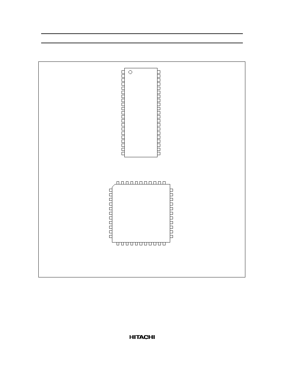
Pin Arrangement
RD /COMP
RD /COMP
TONEC
TONER
VT
ref
RE /VC
ref
TEST
OSC
OSC
RESET
GND
D
D
D
D
D
D
D
D
D
D
0 0
1 1
0
1
2
0
1
2
3
4
5
6
7
8
9
1
2
3
4
5
6
7
8
9
10
11
12
13
14
15
16
17
18
19
20
21
42
41
40
39
38
37
36
35
34
33
32
31
30
29
28
27
26
25
24
23
22
DP-42S
V
SEL
R4 /SO
R4 /SI
R4 /
SCK
R4 /EVND
R3
R3 /TOD
R3 /TOC
R3
R2
R2
R2
R2
R1
R1
R1
R1
R0 /
INT
D /
INT
D /
STOPC
CC
3 1
2 1
1 1
0
3
2
1
0
3
2
1
0
3
2
1
0
0 1
13 0
12
1
2
3
4
5
6
7
8
9
10
11
33
32
31
30
29
28
27
26
25
24
23
44
43
42
41
40
39
38
37
36
35
34
12
13
14
15
16
17
18
19
20
21
22
FP-44A
RE
0
/VC
ref
TEST
OSC
1
OSC
2
RESET
GND
D
0
D
1
D
2
D
3
D
4
R4 /EVND
R3
R3 /TOD
R3 /TOC
R3
R2
R2
R2
R2
R1
R1
0
3
2
1
0
3
2
1
0
3
2
D
D
D
D
D
D /
STOPC
D /
INT
R0 /
INT
R1
R1
NC
5
6
7
8
9
12
13 0
0 1
0
1
NC
VT
ref
TONER
TONEC
RD /COMP
RD /COMP
V
SEL
R4 /SO
R4 /SI
R4 /
SCK
1 1
0 0
CC
3 1
2 1
1 1
(top view)

HD404654 Series
4
Pin Description
Pin Number
Item
Symbol
DP-42S
FP-44A
I/O
Function
Power supply
V
CC
42
38
Applies power voltage
GND
11
6
Connected to ground
Test
TEST
7
2
I
Used for factory testing only: Connect this pin to
V
CC
Reset
RESET
10
5
I
Resets the MCU
Oscillator
OSC
1
8
3
I
OSC
2
9
4
O
Port
D
0
�D
9
12�21
7�16
I/O
Input/output pins addressed by individual bits;
pins D
4
�D
9
are high-current sink pins that can
each supply up to 15 mA, D
0
� D
3
are large-
current source pins that can each supply up to 10
mA
D
12
, D
13
22, 23
17, 18
I
Input pins addressable by individual bits
R0
0
�R4
3
24�40
19�21,
23�36
I/O
Input/output pins addressable in 4-bit units
RD
0
, RD
1
, RE
0
1, 2, 6
39, 40,1
I
Input pins addressable in 4-bit units
Interrupt
INT
0
,
INT
1
23, 24
18, 19
I
Input pins for external interrupts
Stop clear
STOPC
22
17
I
Input pin for transition from stop mode to active
mode
Serial
SCK
1
38
34
I/O
Serial clock input/output pin
SI
1
39
35
I
Serial receive data input pin
SO
1
40
36
O
Serial transmit data output pin
Timer
TOC, TOD
34, 35
30, 31
O
Timer output pins
EVND
37
33
I
Event count input pins
DTMF
TONER
4
42
O
Output pin for DTMF row signals
TONEC
3
41
O
Output pin for DTMF column signals.
VT
ref
5
43
Reference voltage pin for DTMF signals
Voltage condition is V
CC
VT
ref
GND.
Comparator
COMP
0
,
COMP
1
1, 2
39, 40
I
Analog input pins for voltage comparator
VC
ref
6
1
Reference voltage pin for inputting the threshold
voltage of the analog input pin.
Division rate
SEL
41
37
I
Input pin for selecting system clock division rate
rate after
RESET
input or after stop mode
cancellation.
1/4 division rate: Connect it to V
CC
1/32 division rate: Connect it to GND