
HD404358 Series
Rev. 6.0
Sept. 1998
Description
The HD404358 Series is a 4-bit HMCS400-Series microcomputer designed to increase program
productivity and also incorporate large-capacity memory. Each microcomputer has an A/D converter, input
capture timer, and two low-power dissipation modes.
The HD404358 Series includes seven chips: the HD404354, HD40A4354 with 4-kword ROM; the
HD404356, HD40A4356 with 6-kword ROM; the HD404358, HD40A4358 with 8-kword ROM; the
HD407A4359 with 16-kword PROM.
The HD40A4354, HD40A4356, HA40A4358, and HD407A4359 are high speed versions (minimum
instruction cycle time: 0.47
µ
s)
The HD407A4359 is a PROM version (ZTAT
TM
microcomputer). A program can be written to the PROM
by a PROM writer, which can dramatically shorten system development periods and smooth the process
from debugging to mass production. (The ZTAT
TM
version is 27256-compatible.)
ZTAT
TM
: Zero Turn Around Time ZTAT is a trademark of Hitachi Ltd.
Features
∑
34 I/O pins
One input-only pin
33 input/output pins: 4 pins are intermediate-voltage NMOS open drain with high-current pins (15
mA, max.)
∑
On-chip A/D converter (8-bit
◊
8-channel)
Low power voltage 2.7 V to 6.0 V
∑
Three timers
One event counter input
One timer output
One input capture timer
∑
Eight-bit clock-synchronous serial interface (1 channel)
∑
Alarm output

HD404358 Series
2
∑
Built-in oscillators
Ceramic oscillator or crystal
External clock drive is also possible
∑
Seven interrupt sources
Two by external sources
Three by timers
One by A/D converter
One by serial interface
∑
Two low-power dissipation modes
Standby mode
Stop mode
∑
Instruction cycle time
0.47
µ
s (f
OSC
= 8.5 MHz, 1/4 division ratio):
HD40A4354, HD40A4356, HD40A4358,
HD407A4359
0.8
µ
s (f
OSC
= 5 MHz, 1/4 division ratio):
HD404354, HD404356, HD404358
Ordering Information
Type
Instruction Cycle
Time
Product Name
Model Name
ROM
(Words)
RAM
(Digit)
Package
Mask ROM Standard versions
HD404354
HD404354S
4,096
384
DP-42S
(f
OSC
= 5 MHz)
HD404354H
FP-44A
HD404356
HD404356S
6,144
DP-42S
HD404356H
FP-44A
HD404358
HD404358S
8,192
DP-42S
HD404358H
FP-44A
High speed versions HD40A4354
HD40A4354S
4,096
384
DP-42S
(f
OSC
= 8.5 MHz)
HD40A4354H
FP-44A
HD40A4356
HD40A4356S
6,144
DP-42S
HD40A4356H
FP-44A
HD40A4358
HD40A4358S
8,192
DP-42S
HD40A4358H
FP-44A
ZTAT
TM
(f
OSC
= 8.5 MHz)
HD407A4359
HD407A4359S
16,384
512
DP-42S
HD407A4359H
FP-44A

HD404358 Series
3
Pin Arrangement
1
2
3
4
5
6
7
8
9
10
11
33
32
31
30
29
28
27
26
25
24
23
12
13
14
15
16
17
18
19
20
21
22
44
43
42
41
40
39
38
37
36
35
34
FP-44A
TEST
RESET
OSC
1
OSC
2
GND
AV
SS
R3
0
/AN
0
R3
1
/AN
1
R3
2
/AN
2
R3
3
/AN
3
R4
0
/AN
4
R1
2
R8
3
R8
2
R8
1
R8
0
D
8
D
7
D
6
D
5
R1
1
R1
0
NC
R0
3
R0
2
R0
1
R0
0
RA
1
R2
3
R2
2
R2
1
R2
0
R1
3
/
SCK
/SI
/SO
/TOC
R4
1
/AN
5
AV
CC
V
CC
D
0
/
INT
0
D
1
/
INT
1
D
2
/EVNB
D
3
/BUZZ
D
4
/
STOPC
NC
R4
2
/AN
6
R4
3
/AN
7
R0
0
/
SCK
R0
1
/SI
R0
2
/SO
R0
3
/TOC
TEST
RESET
OSC
1
OSC
2
AV
SS
R8
3
R8
2
R8
1
R8
0
D
8
D
7
D
6
D
5
D
4
/
STOPC
D
3
/BUZZ
D
2
/EVNB
D
1
/
INT
1
D
0
/INT
0
RA
1
R2
3
R2
2
R2
1
R2
0
R1
3
R1
2
R1
1
R1
0
DP-42S
1
2
3
4
5
6
7
8
9
10
11
12
13
14
15
16
17
18
19
20
21
29
28
27
26
25
24
23
22
42
41
40
39
38
37
36
35
34
33
32
31
30
V
CC
AV
CC
R3
0
/AN
0
R3
1
/AN
1
R3
2
/AN
2
R3
3
/AN
3
R4
0
/AN
4
R4
1
/AN
5
R4
2
/AN
6
R4
3
/AN
7
GND

HD404358 Series
4
Pin Description
Pin Number
Item
Symbol
DP-42S FP-44A I/O
Function
Power
supply
V
CC
21
16
Applies power voltage
GND
10
5
Connected to ground
Test
TEST
6
1
I
Cannot be used in user applications. Connect this pin
to GND.
Reset
RESET
7
2
I
Resets the MCU
Oscillator
OSC
1
8
3
I
Input/output pin for the internal oscillator. Connect
these pins to the ceramic oscillator or crystal oscillator,
or OSC
1
to an external oscillator circuit.
OSC
2
9
4
O
Port
D
0
≠D
8
22≠30
17≠21,
23≠26
I/O
Input/output pins addressed individually by bits; D
0
≠D
8
are all standard-voltage I/O pins.
RA
1
1
39
I
One-bit standard-voltage input port pin
R0
0
≠R1
3
,
R3
0
≠R4
3
,
R8
0
≠R8
3
2≠5,
12≠19,
31≠38
40≠43,
7≠14
27≠34
I/O
Four-bit input/output pins consisting of standard-voltage
pins
R2
0
≠R2
3
39≠42
35≠38
I/O
Four-bit input/output pins consisting of intermediate
voltage pins
Interrupt
INT
0
,
INT
1
22, 23
17, 18
I
Input pins for external interrupts
Stop clear
STOPC
26
21
I
Input pin for transition from stop mode to active mode
Serial
Interface
SCK
2
40
I/O
Serial interface clock input/output pin
SI
3
41
I
Serial interface receive data input pin
SO
4
42
O
Serial interface transmit data output pin
Timer
TOC
5
43
O
Timer output pin
EVNB
24
19
I
Event count input pin
Alarm
BUZZ
25
20
O
Square waveform output pin
A/D
converter
AV
CC
20
15
Power supply for the A/D converter. Connect this pin
as close as possible to the V
CC
pin and at the same
voltage as V
CC
. If the power supply voltage to be used
for the A/D converter is not equal to V
CC
, connect a 0.1-
µ
F bypass capacitor between the AV
CC
and AV
SS
pins.
(However, this is not necessary when the AV
CC
pin is
directly connected to the V
CC
pin.)
AV
SS
11
6
Ground for the A/D converter. Connect this pin as
close as possible to GND at the same voltage as GND.
AN
0
≠AN
7
12≠19
7≠14
I
Analog input pins for the A/D converter
HD404358 Series
5
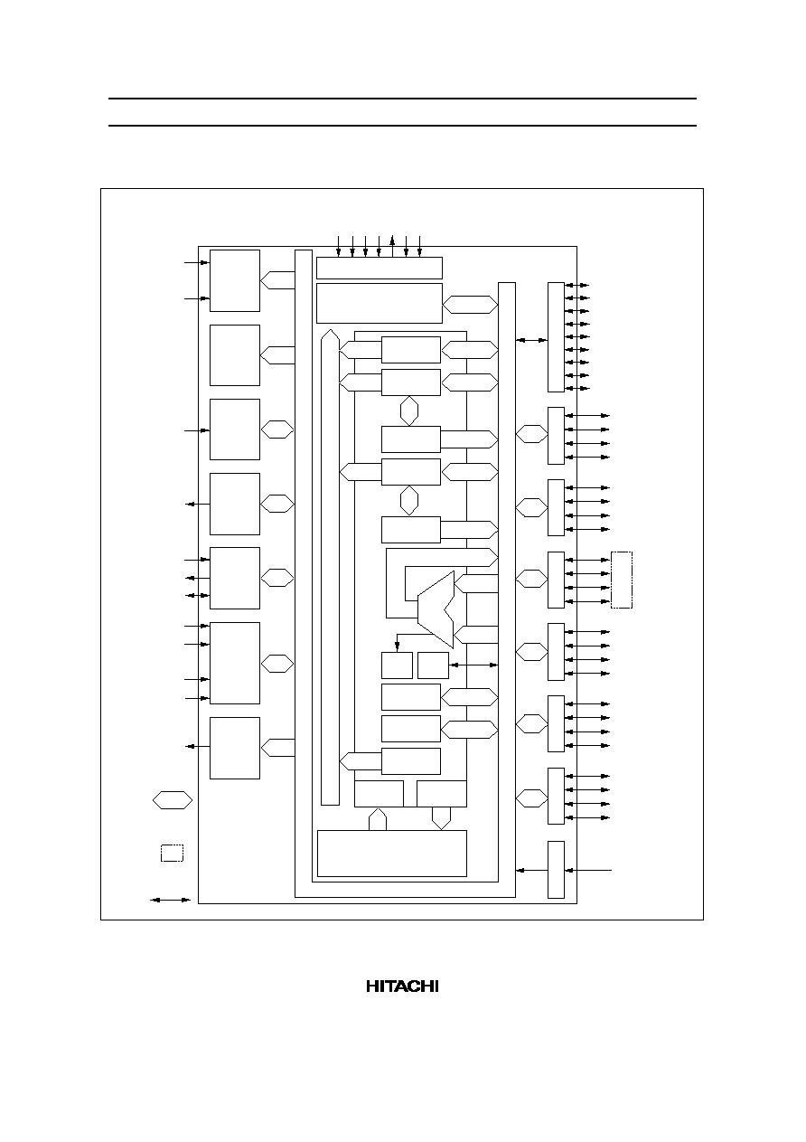
Block Diagram
D
0
D
1
D
2
D
3
D
4
D
5
D
6
D
7
D
8
R0
0
R0
1
R0
2
R0
3
D port
R0 port
R1
0
R1
1
R1
2
R1
3
R1 port
R2
0
R2
1
R2
2
R2
3
R2 port
R3
0
R3
1
R3
2
R3
3
R3 port
R4
0
R4
1
R4
2
R4
3
R4 port
R8
0
R8
1
R8
2
R8
3
R8 port
RA
1
PC
(14 bits)
Instruction
decoder
SP
(10 bits)
B
(4 bits)
A
(4 bits)
ST
(1 bit)
CA
(1 bit)
ALU
SPY
(4 bits)
Y
(4 bits)
SPX
(4 bits)
X
(4 bits)
W
(2 bits)
RAM
(384 4 bits)
(512 4 bits)
System control
Interrupt
control
Timer A
Timer B
Timer C
Serial
interface
A/D
converter
Buzzer
Internal data bus
Internal data bus
Internal address bus
BUZZ
AV
CC
AN
7
AV
SS
AN
0
∑
∑
∑
∑
∑
∑
SI
SO
SCK
TOC
EVNB
INT
0
INT
1
Data bus
Intermediate
voltage pin
Directional
signal line
GND
V
CC
OSC
2
OSC
1
STOPC
TEST
RESET
RA port
ROM
(4,096 10 bits) (6,144 10 bits)
(16,384 10 bits)(8,192 10 bits)
◊
◊
◊
◊
◊
◊