
HD404369 Series
Rev. 6.0
Sept. 1998
Description
The HD404369 Series is a 4-bit HMCS400-Series microcomputer designed to increase program
productivity and also incorporate large-capacity memory. Each microcomputer has an A/D converter, input
capture timer, 32-kHz oscillator for clock, and four low-power dissipation modes.
The HD404369 Series includes nine chips: the HD404364, HD40A4364 with 4-kword ROM; the
HD404368, HD40A4368 with 8-kword ROM; the HD4043612, HD40A43612 with 12-kword ROM; the
HD404369, HD40A4369 with 16-kword ROM; the HD407A4369 with 16-kword PROM.
The HD40A4364, HD40A4368, HD40A43612, HD40A4369, and HD407A4369 are high speed versions
(minimum instruction cycle time: 0.47
µ
s).
The HD407A4369 is a PROM version (ZTAT
TM
microcomputer). A program can be written to the PROM
by a PROM writer, which can dramatically shorten system development periods and smooth the process
from debugging to mass production. (The ZTAT
TM
version is 27256-compatible.)
Features
∑
512-digit
◊
4-bit RAM
∑
54 I/O pins
One input-only pin
53 input/output pins: 8 pins are intermediate-voltage NMOS open drain with high-current pins (15
mA, max.)
∑
On-chip A/D converter (8-bit
◊
12-channel)
Low power voltage 2.7 V to 6.0 V
∑
Three timers
One event counter input
One timer output
One input capture timer
∑
Eight-bit clock-synchronous serial interface (1 channel)
∑
Alarm output

HD404369 Series
2
∑
Built-in oscillators
Ceramic oscillator or crystal
External clock drive is also possible
Subclock: 32.768-kHz crystal oscillator
∑
Seven interrupt sources
Two by external sources
Three by timers
One by A/D converter
One by serial interface
∑
Four low-power dissipation modes
Standby mode
Stop mode
Watch mode
Subactive mode
∑
Instruction cycle time
0.47
µ
s (f
OSC
= 8.5 MHz, 1/4 division ratio):
HD40A4364, HD40A4368, HD40A43612, HD40A4369, HD407A4369
0.8
µ
s (f
OSC
= 5 MHz, 1/4 division ratio):
HD404364, HD404368, HD4043612, HD404369
1/4, 1/8, 1/16, 1/32 system clock division ratio can be selecte
HD404369 Series
3
Ordering Information
Type
Instruction Cycle Time
Product Name
Model Name
ROM (Words) Package
Mask ROM Standard version (f
OSC
= 5 MHz)
HD404364
HD404364S
4,096
DP-64S
HD404364F
FP-64B
HD404364H
FP-64A
HD404368
HD404368S
8,192
DP-64S
HD404368F
FP-64B
HD404368H
FP-64A
HD4043612
HD4043612S
12,288
DP-64S
HD4043612F
FP-64B
HD4043612H
FP-64A
HD404369
HD404369S
16,384
DP-64S
HD404369F
FP-64B
HD404369H
FP-64A
High speed versions
HD40A4364
HD40A4364S
4,096
DP-64S
(f
OSC
= 8.5 MHz)
HD40A4364F
FP-64B
HD40A4364H
FP-64A
HD40A4368
HD40A4368S
8,192
DP-64S
HD40A4368F
FP-64B
HD40A4368H
FP-64A
HD40A43612
HD40A43612S
12,288
DP-64S
HD40A43612F
FP-64B
HD40A43612H
FP-64A
HD40A4369
HD40A4369S
16,384
DP-64S
HD40A4369F
FP-64B
HD40A4369H
FP-64A
ZTAT
TM
(f
OSC
= 8.5 MHz)
HD407A4369
HD407A4369S
16,384
DP-64S
HD407A4369F
FP-64B
HD407A4369H
FP-64A

HD404369 Series
4
Pin Arrangement
1
2
3
4
5
6
7
8
9
10
11
12
13
14
15
16
17
18
19
51
50
49
48
47
46
45
44
43
42
41
40
39
38
37
36
35
34
33
20
21
22
23
24
25
26
27
28
29
30
31
32
64
63
62
61
60
59
58
57
56
55
54
53
52
FP-64B
R7
2
R0
0
/
SCK
R0
1
/SI
R0
2
/SO
R0
3
/TOC
TEST
RESET
OSC
1
OSC
2
GND
X1
X2
AV
SS
R3
0
/AN
0
R3
1
/AN
1
R3
2
/AN
2
R3
3
/AN
3
R4
0
/AN
4
R4
1
/AN
5
R7
1
R7
0
R6
3
R6
2
R6
1
R6
0
RA
1
R2
3
R2
2
R2
1
R2
0
R1
3
R1
2
R4
2
/AN
6
R4
3
/AN
7
R5
0
/AN
8
R5
1
/AN
9
R5
2
/AN
10
R5
3
/AN
11
AV
CC
V
CC
D
0
/
INT
0
D
1
/
INT
1
D
2
/EVNB
D
3
/BUZZ
D
4
/
STOPC
R1
1
R1
0
R9
3
R9
2
R9
1
R9
0
R8
3
R8
2
R8
1
R8
0
D
13
D
12
D
11
D
10
D
9
D
8
D
7
D
6
D
5
R1
0
R9
3
R9
2
R9
1
R9
0
R8
3
R8
2
R8
1
R8
0
D
13
D
12
D
11
D
10
D
9
D
8
D
7
R0
1
/SI
R0
2
/SO
R0
3
/TOC
TEST
RESET
OSC
1
OSC
2
GND
X1
X2
AV
SS
R3
0
/AN
0
R3
1
/AN
1
R3
2
/AN
2
R3
3
/AN
3
R4
0
/AN
4
R0
0
/
SCK
R7
2
R7
1
R7
0
R6
3
R6
2
R6
1
R6
0
RA
1
R2
3
R2
2
R2
1
R2
0
R1
3
R1
2
R1
1
R4
1
/AN
5
R4
2
/AN
6
R4
3
/AN
7
R5
0
/AN
8
R5
1
/AN
9
R5
2
/AN
10
R5
3
/AN
11
AV
CC
V
CC
D
0
/
INT
0
D
1
/
INT
1
D
2
/EVNB
D
3
/BUZZ
D
4
/
STOPC
D
5
D
6
FP-64A
1
2
3
4
5
6
7
8
9
10
11
12
13
14
15
16
48
47
46
45
44
43
42
41
40
39
38
37
36
35
34
33
64
63
62
61
60
59
58
57
56
55
54
53
52
51
50
49
17
18
19
20
21
22
23
24
25
26
27
28
29
30
31
32
R6
0
R6
1
R6
2
R6
3
R7
0
R7
1
R7
2
R0
0
/
SCK
R0
1
/SI
R0
2
/SO
R0
3
/TOC
TEST
RESET
OSC
1
OSC
2
GND
X1
X2
AV
SS
R3
0
/AN
0
R3
1
/AN
1
R3
2
/AN
2
R3
3
/AN
3
R4
0
/AN
4
R4
1
/AN
5
R4
2
/AN
6
R4
3
/AN
7
R5
0
/AN
8
R5
1
/AN
9
R5
2
/AN
10
R5
3
/AN
11
AV
CC
R8
3
R8
2
R8
1
R8
0
D
13
D
12
D
11
D
10
D
9
D
8
D
7
D
6
D
5
D
4
/
STOPC
D
3
/BUZZ
D
2
/EVNB
D
1
/
INT
1
D
0
/
INT
0
V
CC
RA
1
R2
3
R2
2
R2
1
R2
0
R1
3
R1
2
R1
1
R1
0
R9
3
R9
2
R9
1
R9
0
DP-64S
1
2
3
4
5
6
7
8
9
10
11
12
13
14
15
16
17
18
19
20
21
22
23
24
25
26
27
28
29
30
31
32
51
50
49
48
47
46
45
44
43
42
41
40
39
38
37
36
35
34
33
64
63
62
61
60
59
58
57
56
55
54
53
52

HD404369 Series
5
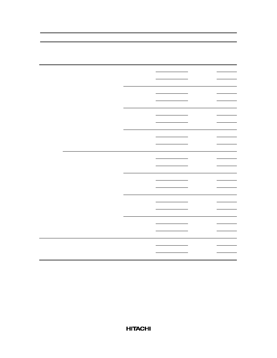
Pin Description
Pin Number
Item
Symbol
DP-64S
FP-64B FP-64A I/O
Function
Power
V
CC
33
27
25
Applies power voltage
Supply
GND
16
10
8
Connected to ground
Test
TEST
12
6
4
I
Cannot be used in user applications. Connect this
pin to GND.
Reset
RESET
13
7
5
I
Resets the MCU
Oscillator OSC
1
14
8
6
I
Input/output pin for the internal oscillator. Connect
these pins to the ceramic oscillator or crystal
oscillator, or OSC
1
to an external oscillator circuit.
OSC
2
15
9
7
O
X1
17
11
9
I
Used with a 32.768-kHz crystal ocillator for clock
purposes
X2
18
12
10
O
Port
D
0
≠D
13
34≠47
28≠41
26≠39
I/O
Input/output pins consisting of standard voltage
pins addressed individually by bits
RA
1
64
58
56
I
One-bit standard-voltage input port pin
R0
0
≠R0
3
,
R3
0
≠R9
3
1≠11,
20≠31,
48≠55
1≠5,
14≠25,
42≠49,
59≠64
1≠3,
12≠23,
40≠47,
57≠64
I/O
Four-bit input/output pins consisting of standard
voltage pins
R1
0
≠R2
3
56≠63
50≠57
48≠55
I/O
Four-bit input/output pins consisting of
intermediate voltage pins
Interrupt
INT
0
,
INT
1
34, 35
28, 29
26, 27
I
Input pins for external interrupts
Stop clear
STOPC
38
32
30
I
Input pin for transition from stop mode to active
mode
Serial
SCK
8
2
64
I/O
Serial interface clock input/output pin
Interface
SI
9
3
1
I
Serial interface receive data input pin
SO
10
4
2
O
Serial interface transmit data output pin
Timer
TOC
11
5
3
O
Timer output pin
EVNB
36
30
28
I
Event count input pin
Alarm
BUZZ
37
31
29
O
Square waveform output pin