
H8/532 Hardware Manual

Preface
The H8/532 is a high-performance single-chip Hitachi-original microcomputer, featuring a high-
speed CPU with 16-bit internal data paths and a full complement of on-chip supporting modules.
The H8/532 is an ideal microcontroller for a wide variety of medium-scale devices, including both
office and industrial equipment and consumer products.
Its highly orthogonal instruction set is designed for fast execution of programs coded in the high-
level C language.
On-chip facilities include large RAM and ROM memories, numerous timers, serial I/O, an A/D
converter, I/O ports, and other functions for compact implementation of high-performance
application systems.
The H8/532 is available in both a ZTAT
TM
version* with on-chip PROM, ideal for the early stages
of production or for products with frequently-changing specifications, and a masked-ROM version
suitable for volume production.
This manual gives a hardware description of the H8/532. For details of the instruction set, refer to
the H8/500 Series Programming Manual, which applies to all chips in the H8/500 Series.
* ZTAT (Zero Turn-Around Time) is a registered trademark of Hitachi, Ltd.

Contents
Section 1 Overview
1.1
Features ∑∑∑∑∑∑∑∑∑∑∑∑∑∑∑∑∑∑∑∑∑∑∑∑∑∑∑∑∑∑∑∑∑∑∑∑∑∑∑∑∑∑∑∑∑∑∑∑∑∑∑∑∑∑∑∑∑∑∑∑∑∑∑∑∑∑∑∑∑∑∑∑∑∑∑∑∑∑∑∑∑∑∑∑∑∑∑∑∑∑∑∑∑∑∑∑∑∑∑∑∑∑∑∑∑∑∑∑∑∑∑∑∑∑∑∑∑∑∑∑∑∑∑∑∑∑∑∑∑∑1
1.2
Block Diagram ∑∑∑∑∑∑∑∑∑∑∑∑∑∑∑∑∑∑∑∑∑∑∑∑∑∑∑∑∑∑∑∑∑∑∑∑∑∑∑∑∑∑∑∑∑∑∑∑∑∑∑∑∑∑∑∑∑∑∑∑∑∑∑∑∑∑∑∑∑∑∑∑∑∑∑∑∑∑∑∑∑∑∑∑∑∑∑∑∑∑∑∑∑∑∑∑∑∑∑∑∑∑∑∑∑∑∑∑∑∑∑∑∑∑∑∑∑∑∑4
1.3
Pin Arrangements and Functions ∑∑∑∑∑∑∑∑∑∑∑∑∑∑∑∑∑∑∑∑∑∑∑∑∑∑∑∑∑∑∑∑∑∑∑∑∑∑∑∑∑∑∑∑∑∑∑∑∑∑∑∑∑∑∑∑∑∑∑∑∑∑∑∑∑∑∑∑∑∑∑∑∑∑∑∑∑∑∑∑∑∑∑∑∑∑∑∑∑∑∑5
1.3.1 Pin Arrangement ∑∑∑∑∑∑∑∑∑∑∑∑∑∑∑∑∑∑∑∑∑∑∑∑∑∑∑∑∑∑∑∑∑∑∑∑∑∑∑∑∑∑∑∑∑∑∑∑∑∑∑∑∑∑∑∑∑∑∑∑∑∑∑∑∑∑∑∑∑∑∑∑∑∑∑∑∑∑∑∑∑∑∑∑∑∑∑∑∑∑∑∑∑∑∑∑∑∑∑∑∑∑∑∑∑5
1.3.2 Pin Functions ∑∑∑∑∑∑∑∑∑∑∑∑∑∑∑∑∑∑∑∑∑∑∑∑∑∑∑∑∑∑∑∑∑∑∑∑∑∑∑∑∑∑∑∑∑∑∑∑∑∑∑∑∑∑∑∑∑∑∑∑∑∑∑∑∑∑∑∑∑∑∑∑∑∑∑∑∑∑∑∑∑∑∑∑∑∑∑∑∑∑∑∑∑∑∑∑∑∑∑∑∑∑∑∑∑∑∑∑∑∑8
Section 2 MCU Operating Modes and Address Space
2.1
Overview ∑∑∑∑∑∑∑∑∑∑∑∑∑∑∑∑∑∑∑∑∑∑∑∑∑∑∑∑∑∑∑∑∑∑∑∑∑∑∑∑∑∑∑∑∑∑∑∑∑∑∑∑∑∑∑∑∑∑∑∑∑∑∑∑∑∑∑∑∑∑∑∑∑∑∑∑∑∑∑∑∑∑∑∑∑∑∑∑∑∑∑∑∑∑∑∑∑∑∑∑∑∑∑∑∑∑∑∑∑∑∑∑∑∑∑∑∑∑∑∑∑∑∑∑∑∑23
2.2
Mode Descriptions ∑∑∑∑∑∑∑∑∑∑∑∑∑∑∑∑∑∑∑∑∑∑∑∑∑∑∑∑∑∑∑∑∑∑∑∑∑∑∑∑∑∑∑∑∑∑∑∑∑∑∑∑∑∑∑∑∑∑∑∑∑∑∑∑∑∑∑∑∑∑∑∑∑∑∑∑∑∑∑∑∑∑∑∑∑∑∑∑∑∑∑∑∑∑∑∑∑∑∑∑∑∑∑∑∑∑∑∑∑∑∑24
2.3
Address Space Map ∑∑∑∑∑∑∑∑∑∑∑∑∑∑∑∑∑∑∑∑∑∑∑∑∑∑∑∑∑∑∑∑∑∑∑∑∑∑∑∑∑∑∑∑∑∑∑∑∑∑∑∑∑∑∑∑∑∑∑∑∑∑∑∑∑∑∑∑∑∑∑∑∑∑∑∑∑∑∑∑∑∑∑∑∑∑∑∑∑∑∑∑∑∑∑∑∑∑∑∑∑∑∑∑∑∑∑∑∑∑25
2.3.1 Page Segmentation ∑∑∑∑∑∑∑∑∑∑∑∑∑∑∑∑∑∑∑∑∑∑∑∑∑∑∑∑∑∑∑∑∑∑∑∑∑∑∑∑∑∑∑∑∑∑∑∑∑∑∑∑∑∑∑∑∑∑∑∑∑∑∑∑∑∑∑∑∑∑∑∑∑∑∑∑∑∑∑∑∑∑∑∑∑∑∑∑∑∑∑∑∑∑∑∑∑∑∑∑25
2.3.2 Page 0 Address Allocations ∑∑∑∑∑∑∑∑∑∑∑∑∑∑∑∑∑∑∑∑∑∑∑∑∑∑∑∑∑∑∑∑∑∑∑∑∑∑∑∑∑∑∑∑∑∑∑∑∑∑∑∑∑∑∑∑∑∑∑∑∑∑∑∑∑∑∑∑∑∑∑∑∑∑∑∑∑∑∑∑∑∑∑∑∑∑27
2.4
Mode Control Register (MDCR) ∑∑∑∑∑∑∑∑∑∑∑∑∑∑∑∑∑∑∑∑∑∑∑∑∑∑∑∑∑∑∑∑∑∑∑∑∑∑∑∑∑∑∑∑∑∑∑∑∑∑∑∑∑∑∑∑∑∑∑∑∑∑∑∑∑∑∑∑∑∑∑∑∑∑∑∑∑∑∑∑∑∑∑∑∑∑∑∑∑29
Section 3 CPU
3.1
Overview ∑∑∑∑∑∑∑∑∑∑∑∑∑∑∑∑∑∑∑∑∑∑∑∑∑∑∑∑∑∑∑∑∑∑∑∑∑∑∑∑∑∑∑∑∑∑∑∑∑∑∑∑∑∑∑∑∑∑∑∑∑∑∑∑∑∑∑∑∑∑∑∑∑∑∑∑∑∑∑∑∑∑∑∑∑∑∑∑∑∑∑∑∑∑∑∑∑∑∑∑∑∑∑∑∑∑∑∑∑∑∑∑∑∑∑∑∑∑∑∑∑∑∑∑∑∑31
3.1.1 Features ∑∑∑∑∑∑∑∑∑∑∑∑∑∑∑∑∑∑∑∑∑∑∑∑∑∑∑∑∑∑∑∑∑∑∑∑∑∑∑∑∑∑∑∑∑∑∑∑∑∑∑∑∑∑∑∑∑∑∑∑∑∑∑∑∑∑∑∑∑∑∑∑∑∑∑∑∑∑∑∑∑∑∑∑∑∑∑∑∑∑∑∑∑∑∑∑∑∑∑∑∑∑∑∑∑∑∑∑∑∑∑∑∑∑∑∑∑31
3.1.2 Address Space ∑∑∑∑∑∑∑∑∑∑∑∑∑∑∑∑∑∑∑∑∑∑∑∑∑∑∑∑∑∑∑∑∑∑∑∑∑∑∑∑∑∑∑∑∑∑∑∑∑∑∑∑∑∑∑∑∑∑∑∑∑∑∑∑∑∑∑∑∑∑∑∑∑∑∑∑∑∑∑∑∑∑∑∑∑∑∑∑∑∑∑∑∑∑∑∑∑∑∑∑∑∑∑∑∑∑∑32
3.1.3 Register Configuration ∑∑∑∑∑∑∑∑∑∑∑∑∑∑∑∑∑∑∑∑∑∑∑∑∑∑∑∑∑∑∑∑∑∑∑∑∑∑∑∑∑∑∑∑∑∑∑∑∑∑∑∑∑∑∑∑∑∑∑∑∑∑∑∑∑∑∑∑∑∑∑∑∑∑∑∑∑∑∑∑∑∑∑∑∑∑∑∑∑∑∑∑∑∑33
3.2
CPU Register Descriptions ∑∑∑∑∑∑∑∑∑∑∑∑∑∑∑∑∑∑∑∑∑∑∑∑∑∑∑∑∑∑∑∑∑∑∑∑∑∑∑∑∑∑∑∑∑∑∑∑∑∑∑∑∑∑∑∑∑∑∑∑∑∑∑∑∑∑∑∑∑∑∑∑∑∑∑∑∑∑∑∑∑∑∑∑∑∑∑∑∑∑∑∑∑∑∑∑∑∑34
3.2.1 General Registers ∑∑∑∑∑∑∑∑∑∑∑∑∑∑∑∑∑∑∑∑∑∑∑∑∑∑∑∑∑∑∑∑∑∑∑∑∑∑∑∑∑∑∑∑∑∑∑∑∑∑∑∑∑∑∑∑∑∑∑∑∑∑∑∑∑∑∑∑∑∑∑∑∑∑∑∑∑∑∑∑∑∑∑∑∑∑∑∑∑∑∑∑∑∑∑∑∑∑∑∑∑∑34
3.2.2 Control Registers ∑∑∑∑∑∑∑∑∑∑∑∑∑∑∑∑∑∑∑∑∑∑∑∑∑∑∑∑∑∑∑∑∑∑∑∑∑∑∑∑∑∑∑∑∑∑∑∑∑∑∑∑∑∑∑∑∑∑∑∑∑∑∑∑∑∑∑∑∑∑∑∑∑∑∑∑∑∑∑∑∑∑∑∑∑∑∑∑∑∑∑∑∑∑∑∑∑∑∑∑∑∑35
3.2.3 Initial Register Values ∑∑∑∑∑∑∑∑∑∑∑∑∑∑∑∑∑∑∑∑∑∑∑∑∑∑∑∑∑∑∑∑∑∑∑∑∑∑∑∑∑∑∑∑∑∑∑∑∑∑∑∑∑∑∑∑∑∑∑∑∑∑∑∑∑∑∑∑∑∑∑∑∑∑∑∑∑∑∑∑∑∑∑∑∑∑∑∑∑∑∑∑∑∑∑40
3.3
Data Formats ∑∑∑∑∑∑∑∑∑∑∑∑∑∑∑∑∑∑∑∑∑∑∑∑∑∑∑∑∑∑∑∑∑∑∑∑∑∑∑∑∑∑∑∑∑∑∑∑∑∑∑∑∑∑∑∑∑∑∑∑∑∑∑∑∑∑∑∑∑∑∑∑∑∑∑∑∑∑∑∑∑∑∑∑∑∑∑∑∑∑∑∑∑∑∑∑∑∑∑∑∑∑∑∑∑∑∑∑∑∑∑∑∑∑∑∑∑∑∑∑41
3.3.1 Data Formats in General Registers ∑∑∑∑∑∑∑∑∑∑∑∑∑∑∑∑∑∑∑∑∑∑∑∑∑∑∑∑∑∑∑∑∑∑∑∑∑∑∑∑∑∑∑∑∑∑∑∑∑∑∑∑∑∑∑∑∑∑∑∑∑∑∑∑∑∑∑∑∑∑∑∑∑∑∑41
3.3.2 Data Formats in Memory ∑∑∑∑∑∑∑∑∑∑∑∑∑∑∑∑∑∑∑∑∑∑∑∑∑∑∑∑∑∑∑∑∑∑∑∑∑∑∑∑∑∑∑∑∑∑∑∑∑∑∑∑∑∑∑∑∑∑∑∑∑∑∑∑∑∑∑∑∑∑∑∑∑∑∑∑∑∑∑∑∑∑∑∑∑∑∑∑∑∑42
3.4
Instructions ∑∑∑∑∑∑∑∑∑∑∑∑∑∑∑∑∑∑∑∑∑∑∑∑∑∑∑∑∑∑∑∑∑∑∑∑∑∑∑∑∑∑∑∑∑∑∑∑∑∑∑∑∑∑∑∑∑∑∑∑∑∑∑∑∑∑∑∑∑∑∑∑∑∑∑∑∑∑∑∑∑∑∑∑∑∑∑∑∑∑∑∑∑∑∑∑∑∑∑∑∑∑∑∑∑∑∑∑∑∑∑∑∑∑∑∑∑∑∑∑∑∑∑44
3.4.1 Basic Instruction Formats ∑∑∑∑∑∑∑∑∑∑∑∑∑∑∑∑∑∑∑∑∑∑∑∑∑∑∑∑∑∑∑∑∑∑∑∑∑∑∑∑∑∑∑∑∑∑∑∑∑∑∑∑∑∑∑∑∑∑∑∑∑∑∑∑∑∑∑∑∑∑∑∑∑∑∑∑∑∑∑∑∑∑∑∑∑∑∑∑∑44
3.4.2 Addressing Modes ∑∑∑∑∑∑∑∑∑∑∑∑∑∑∑∑∑∑∑∑∑∑∑∑∑∑∑∑∑∑∑∑∑∑∑∑∑∑∑∑∑∑∑∑∑∑∑∑∑∑∑∑∑∑∑∑∑∑∑∑∑∑∑∑∑∑∑∑∑∑∑∑∑∑∑∑∑∑∑∑∑∑∑∑∑∑∑∑∑∑∑∑∑∑∑∑∑∑∑∑45
3.4.3 Effective Address Calculation ∑∑∑∑∑∑∑∑∑∑∑∑∑∑∑∑∑∑∑∑∑∑∑∑∑∑∑∑∑∑∑∑∑∑∑∑∑∑∑∑∑∑∑∑∑∑∑∑∑∑∑∑∑∑∑∑∑∑∑∑∑∑∑∑∑∑∑∑∑∑∑∑∑∑∑∑∑∑∑∑∑∑∑47
3.5
Instruction Set ∑∑∑∑∑∑∑∑∑∑∑∑∑∑∑∑∑∑∑∑∑∑∑∑∑∑∑∑∑∑∑∑∑∑∑∑∑∑∑∑∑∑∑∑∑∑∑∑∑∑∑∑∑∑∑∑∑∑∑∑∑∑∑∑∑∑∑∑∑∑∑∑∑∑∑∑∑∑∑∑∑∑∑∑∑∑∑∑∑∑∑∑∑∑∑∑∑∑∑∑∑∑∑∑∑∑∑∑∑∑∑∑∑∑∑∑∑∑50
3.5.1 Overview ∑∑∑∑∑∑∑∑∑∑∑∑∑∑∑∑∑∑∑∑∑∑∑∑∑∑∑∑∑∑∑∑∑∑∑∑∑∑∑∑∑∑∑∑∑∑∑∑∑∑∑∑∑∑∑∑∑∑∑∑∑∑∑∑∑∑∑∑∑∑∑∑∑∑∑∑∑∑∑∑∑∑∑∑∑∑∑∑∑∑∑∑∑∑∑∑∑∑∑∑∑∑∑∑∑∑∑∑∑∑∑∑∑∑∑50
3.5.2 Data Transfer Instructions ∑∑∑∑∑∑∑∑∑∑∑∑∑∑∑∑∑∑∑∑∑∑∑∑∑∑∑∑∑∑∑∑∑∑∑∑∑∑∑∑∑∑∑∑∑∑∑∑∑∑∑∑∑∑∑∑∑∑∑∑∑∑∑∑∑∑∑∑∑∑∑∑∑∑∑∑∑∑∑∑∑∑∑∑∑∑∑∑∑52
3.5.3 Arithmetic Instructions ∑∑∑∑∑∑∑∑∑∑∑∑∑∑∑∑∑∑∑∑∑∑∑∑∑∑∑∑∑∑∑∑∑∑∑∑∑∑∑∑∑∑∑∑∑∑∑∑∑∑∑∑∑∑∑∑∑∑∑∑∑∑∑∑∑∑∑∑∑∑∑∑∑∑∑∑∑∑∑∑∑∑∑∑∑∑∑∑∑∑∑∑∑53
3.5.4 Logic Operations ∑∑∑∑∑∑∑∑∑∑∑∑∑∑∑∑∑∑∑∑∑∑∑∑∑∑∑∑∑∑∑∑∑∑∑∑∑∑∑∑∑∑∑∑∑∑∑∑∑∑∑∑∑∑∑∑∑∑∑∑∑∑∑∑∑∑∑∑∑∑∑∑∑∑∑∑∑∑∑∑∑∑∑∑∑∑∑∑∑∑∑∑∑∑∑∑∑∑∑∑∑∑∑54
3.5.5 Shift Operations ∑∑∑∑∑∑∑∑∑∑∑∑∑∑∑∑∑∑∑∑∑∑∑∑∑∑∑∑∑∑∑∑∑∑∑∑∑∑∑∑∑∑∑∑∑∑∑∑∑∑∑∑∑∑∑∑∑∑∑∑∑∑∑∑∑∑∑∑∑∑∑∑∑∑∑∑∑∑∑∑∑∑∑∑∑∑∑∑∑∑∑∑∑∑∑∑∑∑∑∑∑∑∑∑55
3.5.6 Bit Manipulations ∑∑∑∑∑∑∑∑∑∑∑∑∑∑∑∑∑∑∑∑∑∑∑∑∑∑∑∑∑∑∑∑∑∑∑∑∑∑∑∑∑∑∑∑∑∑∑∑∑∑∑∑∑∑∑∑∑∑∑∑∑∑∑∑∑∑∑∑∑∑∑∑∑∑∑∑∑∑∑∑∑∑∑∑∑∑∑∑∑∑∑∑∑∑∑∑∑∑∑∑∑∑56
3.5.7 Branching Instructions ∑∑∑∑∑∑∑∑∑∑∑∑∑∑∑∑∑∑∑∑∑∑∑∑∑∑∑∑∑∑∑∑∑∑∑∑∑∑∑∑∑∑∑∑∑∑∑∑∑∑∑∑∑∑∑∑∑∑∑∑∑∑∑∑∑∑∑∑∑∑∑∑∑∑∑∑∑∑∑∑∑∑∑∑∑∑∑∑∑∑∑∑∑∑57

3.5.8 System Control Instructions ∑∑∑∑∑∑∑∑∑∑∑∑∑∑∑∑∑∑∑∑∑∑∑∑∑∑∑∑∑∑∑∑∑∑∑∑∑∑∑∑∑∑∑∑∑∑∑∑∑∑∑∑∑∑∑∑∑∑∑∑∑∑∑∑∑∑∑∑∑∑∑∑∑∑∑∑∑∑∑∑∑∑∑∑∑∑59
3.5.9 Short-Format Instructions ∑∑∑∑∑∑∑∑∑∑∑∑∑∑∑∑∑∑∑∑∑∑∑∑∑∑∑∑∑∑∑∑∑∑∑∑∑∑∑∑∑∑∑∑∑∑∑∑∑∑∑∑∑∑∑∑∑∑∑∑∑∑∑∑∑∑∑∑∑∑∑∑∑∑∑∑∑∑∑∑∑∑∑∑∑∑∑∑∑62
3.6
Operating Modes ∑∑∑∑∑∑∑∑∑∑∑∑∑∑∑∑∑∑∑∑∑∑∑∑∑∑∑∑∑∑∑∑∑∑∑∑∑∑∑∑∑∑∑∑∑∑∑∑∑∑∑∑∑∑∑∑∑∑∑∑∑∑∑∑∑∑∑∑∑∑∑∑∑∑∑∑∑∑∑∑∑∑∑∑∑∑∑∑∑∑∑∑∑∑∑∑∑∑∑∑∑∑∑∑∑∑∑∑∑∑∑∑∑∑62
3.6.1 Minimum Mode ∑∑∑∑∑∑∑∑∑∑∑∑∑∑∑∑∑∑∑∑∑∑∑∑∑∑∑∑∑∑∑∑∑∑∑∑∑∑∑∑∑∑∑∑∑∑∑∑∑∑∑∑∑∑∑∑∑∑∑∑∑∑∑∑∑∑∑∑∑∑∑∑∑∑∑∑∑∑∑∑∑∑∑∑∑∑∑∑∑∑∑∑∑∑∑∑∑∑∑∑∑∑∑∑62
3.6.2 Maximum Mode ∑∑∑∑∑∑∑∑∑∑∑∑∑∑∑∑∑∑∑∑∑∑∑∑∑∑∑∑∑∑∑∑∑∑∑∑∑∑∑∑∑∑∑∑∑∑∑∑∑∑∑∑∑∑∑∑∑∑∑∑∑∑∑∑∑∑∑∑∑∑∑∑∑∑∑∑∑∑∑∑∑∑∑∑∑∑∑∑∑∑∑∑∑∑∑∑∑∑∑∑∑∑∑∑63
3.7
Basic Operational Timing ∑∑∑∑∑∑∑∑∑∑∑∑∑∑∑∑∑∑∑∑∑∑∑∑∑∑∑∑∑∑∑∑∑∑∑∑∑∑∑∑∑∑∑∑∑∑∑∑∑∑∑∑∑∑∑∑∑∑∑∑∑∑∑∑∑∑∑∑∑∑∑∑∑∑∑∑∑∑∑∑∑∑∑∑∑∑∑∑∑∑∑∑∑∑∑∑∑∑∑∑63
3.7.1 Overview ∑∑∑∑∑∑∑∑∑∑∑∑∑∑∑∑∑∑∑∑∑∑∑∑∑∑∑∑∑∑∑∑∑∑∑∑∑∑∑∑∑∑∑∑∑∑∑∑∑∑∑∑∑∑∑∑∑∑∑∑∑∑∑∑∑∑∑∑∑∑∑∑∑∑∑∑∑∑∑∑∑∑∑∑∑∑∑∑∑∑∑∑∑∑∑∑∑∑∑∑∑∑∑∑∑∑∑∑∑∑∑∑∑∑∑63
3.7.2 On-Chip Memory Access Cycle ∑∑∑∑∑∑∑∑∑∑∑∑∑∑∑∑∑∑∑∑∑∑∑∑∑∑∑∑∑∑∑∑∑∑∑∑∑∑∑∑∑∑∑∑∑∑∑∑∑∑∑∑∑∑∑∑∑∑∑∑∑∑∑∑∑∑∑∑∑∑∑∑∑∑∑∑∑∑∑64
3.7.3 Pin States during On-Chip Memory Access ∑∑∑∑∑∑∑∑∑∑∑∑∑∑∑∑∑∑∑∑∑∑∑∑∑∑∑∑∑∑∑∑∑∑∑∑∑∑∑∑∑∑∑∑∑∑∑∑∑∑∑∑∑∑∑∑∑∑∑∑∑65
3.7.4 Register Field Access Cycle (Addresses H'FF80 to H'FFFF) ∑∑∑∑∑∑∑∑∑∑∑∑∑∑∑∑∑∑∑∑∑∑∑∑∑∑∑∑∑∑∑∑∑∑∑66
3.7.5 Pin States during Register Field Access (Addresses H'FF80 to H'FFFF) ∑∑∑∑∑∑∑∑∑∑∑∑∑∑∑∑∑67
3.7.6 External Access Cycle ∑∑∑∑∑∑∑∑∑∑∑∑∑∑∑∑∑∑∑∑∑∑∑∑∑∑∑∑∑∑∑∑∑∑∑∑∑∑∑∑∑∑∑∑∑∑∑∑∑∑∑∑∑∑∑∑∑∑∑∑∑∑∑∑∑∑∑∑∑∑∑∑∑∑∑∑∑∑∑∑∑∑∑∑∑∑∑∑∑∑∑∑∑∑∑68
3.8
CPU States ∑∑∑∑∑∑∑∑∑∑∑∑∑∑∑∑∑∑∑∑∑∑∑∑∑∑∑∑∑∑∑∑∑∑∑∑∑∑∑∑∑∑∑∑∑∑∑∑∑∑∑∑∑∑∑∑∑∑∑∑∑∑∑∑∑∑∑∑∑∑∑∑∑∑∑∑∑∑∑∑∑∑∑∑∑∑∑∑∑∑∑∑∑∑∑∑∑∑∑∑∑∑∑∑∑∑∑∑∑∑∑∑∑∑∑∑∑∑∑∑∑∑∑69
3.8.1 Overview ∑∑∑∑∑∑∑∑∑∑∑∑∑∑∑∑∑∑∑∑∑∑∑∑∑∑∑∑∑∑∑∑∑∑∑∑∑∑∑∑∑∑∑∑∑∑∑∑∑∑∑∑∑∑∑∑∑∑∑∑∑∑∑∑∑∑∑∑∑∑∑∑∑∑∑∑∑∑∑∑∑∑∑∑∑∑∑∑∑∑∑∑∑∑∑∑∑∑∑∑∑∑∑∑∑∑∑∑∑∑∑∑∑∑∑69
3.8.2 Program Execution State ∑∑∑∑∑∑∑∑∑∑∑∑∑∑∑∑∑∑∑∑∑∑∑∑∑∑∑∑∑∑∑∑∑∑∑∑∑∑∑∑∑∑∑∑∑∑∑∑∑∑∑∑∑∑∑∑∑∑∑∑∑∑∑∑∑∑∑∑∑∑∑∑∑∑∑∑∑∑∑∑∑∑∑∑∑∑∑∑∑∑∑71
3.8.3 Exception-Handling State ∑∑∑∑∑∑∑∑∑∑∑∑∑∑∑∑∑∑∑∑∑∑∑∑∑∑∑∑∑∑∑∑∑∑∑∑∑∑∑∑∑∑∑∑∑∑∑∑∑∑∑∑∑∑∑∑∑∑∑∑∑∑∑∑∑∑∑∑∑∑∑∑∑∑∑∑∑∑∑∑∑∑∑∑∑∑∑∑∑71
3.8.4 Bus-Released State ∑∑∑∑∑∑∑∑∑∑∑∑∑∑∑∑∑∑∑∑∑∑∑∑∑∑∑∑∑∑∑∑∑∑∑∑∑∑∑∑∑∑∑∑∑∑∑∑∑∑∑∑∑∑∑∑∑∑∑∑∑∑∑∑∑∑∑∑∑∑∑∑∑∑∑∑∑∑∑∑∑∑∑∑∑∑∑∑∑∑∑∑∑∑∑∑∑∑∑∑72
3.8.5 Reset State ∑∑∑∑∑∑∑∑∑∑∑∑∑∑∑∑∑∑∑∑∑∑∑∑∑∑∑∑∑∑∑∑∑∑∑∑∑∑∑∑∑∑∑∑∑∑∑∑∑∑∑∑∑∑∑∑∑∑∑∑∑∑∑∑∑∑∑∑∑∑∑∑∑∑∑∑∑∑∑∑∑∑∑∑∑∑∑∑∑∑∑∑∑∑∑∑∑∑∑∑∑∑∑∑∑∑∑∑∑∑∑∑∑77
3.8.6 Power-Down State ∑∑∑∑∑∑∑∑∑∑∑∑∑∑∑∑∑∑∑∑∑∑∑∑∑∑∑∑∑∑∑∑∑∑∑∑∑∑∑∑∑∑∑∑∑∑∑∑∑∑∑∑∑∑∑∑∑∑∑∑∑∑∑∑∑∑∑∑∑∑∑∑∑∑∑∑∑∑∑∑∑∑∑∑∑∑∑∑∑∑∑∑∑∑∑∑∑∑∑∑77
3.9
Programming Notes ∑∑∑∑∑∑∑∑∑∑∑∑∑∑∑∑∑∑∑∑∑∑∑∑∑∑∑∑∑∑∑∑∑∑∑∑∑∑∑∑∑∑∑∑∑∑∑∑∑∑∑∑∑∑∑∑∑∑∑∑∑∑∑∑∑∑∑∑∑∑∑∑∑∑∑∑∑∑∑∑∑∑∑∑∑∑∑∑∑∑∑∑∑∑∑∑∑∑∑∑∑∑∑∑∑∑∑∑∑78
3.9.1 Restriction on Address Location ∑∑∑∑∑∑∑∑∑∑∑∑∑∑∑∑∑∑∑∑∑∑∑∑∑∑∑∑∑∑∑∑∑∑∑∑∑∑∑∑∑∑∑∑∑∑∑∑∑∑∑∑∑∑∑∑∑∑∑∑∑∑∑∑∑∑∑∑∑∑∑∑∑∑∑∑∑∑∑78
3.9.2 Note on MULXU Instruction∑∑∑∑∑∑∑∑∑∑∑∑∑∑∑∑∑∑∑∑∑∑∑∑∑∑∑∑∑∑∑∑∑∑∑∑∑∑∑∑∑∑∑∑∑∑∑∑∑∑∑∑∑∑∑∑∑∑∑∑∑∑∑∑∑∑∑∑∑∑∑∑∑∑∑∑∑∑∑∑∑∑∑∑∑79
Section 4 Exception Handling
4.1
Overview ∑∑∑∑∑∑∑∑∑∑∑∑∑∑∑∑∑∑∑∑∑∑∑∑∑∑∑∑∑∑∑∑∑∑∑∑∑∑∑∑∑∑∑∑∑∑∑∑∑∑∑∑∑∑∑∑∑∑∑∑∑∑∑∑∑∑∑∑∑∑∑∑∑∑∑∑∑∑∑∑∑∑∑∑∑∑∑∑∑∑∑∑∑∑∑∑∑∑∑∑∑∑∑∑∑∑∑∑∑∑∑∑∑∑∑∑∑∑∑∑∑∑∑∑∑∑81
4.1.1 Types of Exception Handling and Their Priority ∑∑∑∑∑∑∑∑∑∑∑∑∑∑∑∑∑∑∑∑∑∑∑∑∑∑∑∑∑∑∑∑∑∑∑∑∑∑∑∑∑∑∑∑∑∑∑∑∑∑∑∑∑∑81
4.1.2 Hardware Exception-Handling Sequence ∑∑∑∑∑∑∑∑∑∑∑∑∑∑∑∑∑∑∑∑∑∑∑∑∑∑∑∑∑∑∑∑∑∑∑∑∑∑∑∑∑∑∑∑∑∑∑∑∑∑∑∑∑∑∑∑∑∑∑∑∑∑∑∑∑82
4.1.3 Exception Factors and Vector Table ∑∑∑∑∑∑∑∑∑∑∑∑∑∑∑∑∑∑∑∑∑∑∑∑∑∑∑∑∑∑∑∑∑∑∑∑∑∑∑∑∑∑∑∑∑∑∑∑∑∑∑∑∑∑∑∑∑∑∑∑∑∑∑∑∑∑∑∑∑∑∑∑∑∑82
4.2
Reset ∑∑∑∑∑∑∑∑∑∑∑∑∑∑∑∑∑∑∑∑∑∑∑∑∑∑∑∑∑∑∑∑∑∑∑∑∑∑∑∑∑∑∑∑∑∑∑∑∑∑∑∑∑∑∑∑∑∑∑∑∑∑∑∑∑∑∑∑∑∑∑∑∑∑∑∑∑∑∑∑∑∑∑∑∑∑∑∑∑∑∑∑∑∑∑∑∑∑∑∑∑∑∑∑∑∑∑∑∑∑∑∑∑∑∑∑∑∑∑∑∑∑∑∑∑∑∑∑∑∑∑∑85
4.2.1 Overview ∑∑∑∑∑∑∑∑∑∑∑∑∑∑∑∑∑∑∑∑∑∑∑∑∑∑∑∑∑∑∑∑∑∑∑∑∑∑∑∑∑∑∑∑∑∑∑∑∑∑∑∑∑∑∑∑∑∑∑∑∑∑∑∑∑∑∑∑∑∑∑∑∑∑∑∑∑∑∑∑∑∑∑∑∑∑∑∑∑∑∑∑∑∑∑∑∑∑∑∑∑∑∑∑∑∑∑∑∑∑∑∑∑∑∑85
4.2.2 Reset Sequence ∑∑∑∑∑∑∑∑∑∑∑∑∑∑∑∑∑∑∑∑∑∑∑∑∑∑∑∑∑∑∑∑∑∑∑∑∑∑∑∑∑∑∑∑∑∑∑∑∑∑∑∑∑∑∑∑∑∑∑∑∑∑∑∑∑∑∑∑∑∑∑∑∑∑∑∑∑∑∑∑∑∑∑∑∑∑∑∑∑∑∑∑∑∑∑∑∑∑∑∑∑∑∑∑∑85
4.2.3 Stack Pointer Initialization ∑∑∑∑∑∑∑∑∑∑∑∑∑∑∑∑∑∑∑∑∑∑∑∑∑∑∑∑∑∑∑∑∑∑∑∑∑∑∑∑∑∑∑∑∑∑∑∑∑∑∑∑∑∑∑∑∑∑∑∑∑∑∑∑∑∑∑∑∑∑∑∑∑∑∑∑∑∑∑∑∑∑∑∑∑∑∑∑86
4.3
Address Error ∑∑∑∑∑∑∑∑∑∑∑∑∑∑∑∑∑∑∑∑∑∑∑∑∑∑∑∑∑∑∑∑∑∑∑∑∑∑∑∑∑∑∑∑∑∑∑∑∑∑∑∑∑∑∑∑∑∑∑∑∑∑∑∑∑∑∑∑∑∑∑∑∑∑∑∑∑∑∑∑∑∑∑∑∑∑∑∑∑∑∑∑∑∑∑∑∑∑∑∑∑∑∑∑∑∑∑∑∑∑∑∑∑∑∑∑∑∑∑89
4.3.1 Illegal Instruction Prefetch ∑∑∑∑∑∑∑∑∑∑∑∑∑∑∑∑∑∑∑∑∑∑∑∑∑∑∑∑∑∑∑∑∑∑∑∑∑∑∑∑∑∑∑∑∑∑∑∑∑∑∑∑∑∑∑∑∑∑∑∑∑∑∑∑∑∑∑∑∑∑∑∑∑∑∑∑∑∑∑∑∑∑∑∑∑∑∑∑89
4.3.2 Word Data Access at Odd Address ∑∑∑∑∑∑∑∑∑∑∑∑∑∑∑∑∑∑∑∑∑∑∑∑∑∑∑∑∑∑∑∑∑∑∑∑∑∑∑∑∑∑∑∑∑∑∑∑∑∑∑∑∑∑∑∑∑∑∑∑∑∑∑∑∑∑∑∑∑∑∑∑∑∑∑89
4.3.3 Off-Chip Address Access in Single-Chip Mode ∑∑∑∑∑∑∑∑∑∑∑∑∑∑∑∑∑∑∑∑∑∑∑∑∑∑∑∑∑∑∑∑∑∑∑∑∑∑∑∑∑∑∑∑∑∑∑∑∑∑∑∑∑∑∑89
4.4
Trace ∑∑∑∑∑∑∑∑∑∑∑∑∑∑∑∑∑∑∑∑∑∑∑∑∑∑∑∑∑∑∑∑∑∑∑∑∑∑∑∑∑∑∑∑∑∑∑∑∑∑∑∑∑∑∑∑∑∑∑∑∑∑∑∑∑∑∑∑∑∑∑∑∑∑∑∑∑∑∑∑∑∑∑∑∑∑∑∑∑∑∑∑∑∑∑∑∑∑∑∑∑∑∑∑∑∑∑∑∑∑∑∑∑∑∑∑∑∑∑∑∑∑∑∑∑∑∑∑∑∑∑∑90
4.5
Interrupts ∑∑∑∑∑∑∑∑∑∑∑∑∑∑∑∑∑∑∑∑∑∑∑∑∑∑∑∑∑∑∑∑∑∑∑∑∑∑∑∑∑∑∑∑∑∑∑∑∑∑∑∑∑∑∑∑∑∑∑∑∑∑∑∑∑∑∑∑∑∑∑∑∑∑∑∑∑∑∑∑∑∑∑∑∑∑∑∑∑∑∑∑∑∑∑∑∑∑∑∑∑∑∑∑∑∑∑∑∑∑∑∑∑∑∑∑∑∑∑∑∑∑∑∑∑∑90
4.6
Invalid Instruction ∑∑∑∑∑∑∑∑∑∑∑∑∑∑∑∑∑∑∑∑∑∑∑∑∑∑∑∑∑∑∑∑∑∑∑∑∑∑∑∑∑∑∑∑∑∑∑∑∑∑∑∑∑∑∑∑∑∑∑∑∑∑∑∑∑∑∑∑∑∑∑∑∑∑∑∑∑∑∑∑∑∑∑∑∑∑∑∑∑∑∑∑∑∑∑∑∑∑∑∑∑∑∑∑∑∑∑∑∑∑∑∑92
4.7
Trap Instructions and Zero Divide ∑∑∑∑∑∑∑∑∑∑∑∑∑∑∑∑∑∑∑∑∑∑∑∑∑∑∑∑∑∑∑∑∑∑∑∑∑∑∑∑∑∑∑∑∑∑∑∑∑∑∑∑∑∑∑∑∑∑∑∑∑∑∑∑∑∑∑∑∑∑∑∑∑∑∑∑∑∑∑∑∑∑∑∑∑∑∑92
4.8
Cases in Which Exception Handling is Deferred ∑∑∑∑∑∑∑∑∑∑∑∑∑∑∑∑∑∑∑∑∑∑∑∑∑∑∑∑∑∑∑∑∑∑∑∑∑∑∑∑∑∑∑∑∑∑∑∑∑∑∑∑∑∑∑∑∑∑∑∑∑∑∑∑∑92

4.8.1 Instructions that Disable Interrupts ∑∑∑∑∑∑∑∑∑∑∑∑∑∑∑∑∑∑∑∑∑∑∑∑∑∑∑∑∑∑∑∑∑∑∑∑∑∑∑∑∑∑∑∑∑∑∑∑∑∑∑∑∑∑∑∑∑∑∑∑∑∑∑∑∑∑∑∑∑∑∑∑∑∑∑92
4.8.2 Disabling of Exceptions Immediately after a Reset ∑∑∑∑∑∑∑∑∑∑∑∑∑∑∑∑∑∑∑∑∑∑∑∑∑∑∑∑∑∑∑∑∑∑∑∑∑∑∑∑∑∑∑∑∑∑∑∑∑∑93
4.8.3 Disabling of Interrupts after a Data Transfer Cycle ∑∑∑∑∑∑∑∑∑∑∑∑∑∑∑∑∑∑∑∑∑∑∑∑∑∑∑∑∑∑∑∑∑∑∑∑∑∑∑∑∑∑∑∑∑∑∑∑∑∑93
4.9
Stack Status after Completion of Exception Handling ∑∑∑∑∑∑∑∑∑∑∑∑∑∑∑∑∑∑∑∑∑∑∑∑∑∑∑∑∑∑∑∑∑∑∑∑∑∑∑∑∑∑∑∑∑∑∑∑∑∑∑∑∑∑∑∑94
4.9.1 PC Value Pushed on Stack for Trace,
Interrupts, Trap Instructions, and Zero Divide Exceptions ∑∑∑∑∑∑∑∑∑∑∑∑∑∑∑∑∑∑∑∑∑∑∑∑∑∑∑∑∑∑∑∑∑∑∑∑∑∑∑96
4.9.2 PC Value Pushed on Stack for Address Error and Invalid
Instruction Exceptions ∑∑∑∑∑∑∑∑∑∑∑∑∑∑∑∑∑∑∑∑∑∑∑∑∑∑∑∑∑∑∑∑∑∑∑∑∑∑∑∑∑∑∑∑∑∑∑∑∑∑∑∑∑∑∑∑∑∑∑∑∑∑∑∑∑∑∑∑∑∑∑∑∑∑∑∑∑∑∑∑∑∑∑∑∑∑∑∑∑∑∑∑∑∑96
4.10 Notes on Use of the Stack ∑∑∑∑∑∑∑∑∑∑∑∑∑∑∑∑∑∑∑∑∑∑∑∑∑∑∑∑∑∑∑∑∑∑∑∑∑∑∑∑∑∑∑∑∑∑∑∑∑∑∑∑∑∑∑∑∑∑∑∑∑∑∑∑∑∑∑∑∑∑∑∑∑∑∑∑∑∑∑∑∑∑∑∑∑∑∑∑∑∑∑∑∑∑∑∑∑∑∑∑96
Section 5 Interrupt Controller
5.1
Overview ∑∑∑∑∑∑∑∑∑∑∑∑∑∑∑∑∑∑∑∑∑∑∑∑∑∑∑∑∑∑∑∑∑∑∑∑∑∑∑∑∑∑∑∑∑∑∑∑∑∑∑∑∑∑∑∑∑∑∑∑∑∑∑∑∑∑∑∑∑∑∑∑∑∑∑∑∑∑∑∑∑∑∑∑∑∑∑∑∑∑∑∑∑∑∑∑∑∑∑∑∑∑∑∑∑∑∑∑∑∑∑∑∑∑∑∑∑∑∑∑∑∑∑∑∑∑97
5.1.1 Features ∑∑∑∑∑∑∑∑∑∑∑∑∑∑∑∑∑∑∑∑∑∑∑∑∑∑∑∑∑∑∑∑∑∑∑∑∑∑∑∑∑∑∑∑∑∑∑∑∑∑∑∑∑∑∑∑∑∑∑∑∑∑∑∑∑∑∑∑∑∑∑∑∑∑∑∑∑∑∑∑∑∑∑∑∑∑∑∑∑∑∑∑∑∑∑∑∑∑∑∑∑∑∑∑∑∑∑∑∑∑∑∑∑∑∑∑∑97
5.1.2 Block Diagram ∑∑∑∑∑∑∑∑∑∑∑∑∑∑∑∑∑∑∑∑∑∑∑∑∑∑∑∑∑∑∑∑∑∑∑∑∑∑∑∑∑∑∑∑∑∑∑∑∑∑∑∑∑∑∑∑∑∑∑∑∑∑∑∑∑∑∑∑∑∑∑∑∑∑∑∑∑∑∑∑∑∑∑∑∑∑∑∑∑∑∑∑∑∑∑∑∑∑∑∑∑∑∑∑∑∑98
5.1.3 Register Configuration ∑∑∑∑∑∑∑∑∑∑∑∑∑∑∑∑∑∑∑∑∑∑∑∑∑∑∑∑∑∑∑∑∑∑∑∑∑∑∑∑∑∑∑∑∑∑∑∑∑∑∑∑∑∑∑∑∑∑∑∑∑∑∑∑∑∑∑∑∑∑∑∑∑∑∑∑∑∑∑∑∑∑∑∑∑∑∑∑∑∑∑∑∑∑99
5.2
Interrupt Types ∑∑∑∑∑∑∑∑∑∑∑∑∑∑∑∑∑∑∑∑∑∑∑∑∑∑∑∑∑∑∑∑∑∑∑∑∑∑∑∑∑∑∑∑∑∑∑∑∑∑∑∑∑∑∑∑∑∑∑∑∑∑∑∑∑∑∑∑∑∑∑∑∑∑∑∑∑∑∑∑∑∑∑∑∑∑∑∑∑∑∑∑∑∑∑∑∑∑∑∑∑∑∑∑∑∑∑∑∑∑∑∑∑∑∑∑∑99
5.2.1 External Interrupts ∑∑∑∑∑∑∑∑∑∑∑∑∑∑∑∑∑∑∑∑∑∑∑∑∑∑∑∑∑∑∑∑∑∑∑∑∑∑∑∑∑∑∑∑∑∑∑∑∑∑∑∑∑∑∑∑∑∑∑∑∑∑∑∑∑∑∑∑∑∑∑∑∑∑∑∑∑∑∑∑∑∑∑∑∑∑∑∑∑∑∑∑∑∑∑∑∑∑∑∑99
5.2.2 Internal Interrupts ∑∑∑∑∑∑∑∑∑∑∑∑∑∑∑∑∑∑∑∑∑∑∑∑∑∑∑∑∑∑∑∑∑∑∑∑∑∑∑∑∑∑∑∑∑∑∑∑∑∑∑∑∑∑∑∑∑∑∑∑∑∑∑∑∑∑∑∑∑∑∑∑∑∑∑∑∑∑∑∑∑∑∑∑∑∑∑∑∑∑∑∑∑∑∑∑∑∑∑∑101
5.2.3 Interrupt Vector Table ∑∑∑∑∑∑∑∑∑∑∑∑∑∑∑∑∑∑∑∑∑∑∑∑∑∑∑∑∑∑∑∑∑∑∑∑∑∑∑∑∑∑∑∑∑∑∑∑∑∑∑∑∑∑∑∑∑∑∑∑∑∑∑∑∑∑∑∑∑∑∑∑∑∑∑∑∑∑∑∑∑∑∑∑∑∑∑∑∑∑∑∑∑101
5.3
Register Descriptions ∑∑∑∑∑∑∑∑∑∑∑∑∑∑∑∑∑∑∑∑∑∑∑∑∑∑∑∑∑∑∑∑∑∑∑∑∑∑∑∑∑∑∑∑∑∑∑∑∑∑∑∑∑∑∑∑∑∑∑∑∑∑∑∑∑∑∑∑∑∑∑∑∑∑∑∑∑∑∑∑∑∑∑∑∑∑∑∑∑∑∑∑∑∑∑∑∑∑∑∑∑∑∑∑∑103
5.3.1 Interrupt Priority Registers A to D (IPRA to IPRD) ∑∑∑∑∑∑∑∑∑∑∑∑∑∑∑∑∑∑∑∑∑∑∑∑∑∑∑∑∑∑∑∑∑∑∑∑∑∑∑∑∑∑∑∑∑∑∑103
5.3.2 Timing of Priority Setting ∑∑∑∑∑∑∑∑∑∑∑∑∑∑∑∑∑∑∑∑∑∑∑∑∑∑∑∑∑∑∑∑∑∑∑∑∑∑∑∑∑∑∑∑∑∑∑∑∑∑∑∑∑∑∑∑∑∑∑∑∑∑∑∑∑∑∑∑∑∑∑∑∑∑∑∑∑∑∑∑∑∑∑∑∑∑∑104
5.4
Interrupt Handling Sequence ∑∑∑∑∑∑∑∑∑∑∑∑∑∑∑∑∑∑∑∑∑∑∑∑∑∑∑∑∑∑∑∑∑∑∑∑∑∑∑∑∑∑∑∑∑∑∑∑∑∑∑∑∑∑∑∑∑∑∑∑∑∑∑∑∑∑∑∑∑∑∑∑∑∑∑∑∑∑∑∑∑∑∑∑∑∑∑∑∑∑∑∑∑104
5.4.1 Interrupt Handling Flow ∑∑∑∑∑∑∑∑∑∑∑∑∑∑∑∑∑∑∑∑∑∑∑∑∑∑∑∑∑∑∑∑∑∑∑∑∑∑∑∑∑∑∑∑∑∑∑∑∑∑∑∑∑∑∑∑∑∑∑∑∑∑∑∑∑∑∑∑∑∑∑∑∑∑∑∑∑∑∑∑∑∑∑∑∑∑∑∑∑∑104
5.4.2 Stack Status after Interrupt Handling Sequence ∑∑∑∑∑∑∑∑∑∑∑∑∑∑∑∑∑∑∑∑∑∑∑∑∑∑∑∑∑∑∑∑∑∑∑∑∑∑∑∑∑∑∑∑∑∑∑∑∑∑∑∑∑107
5.4.3 Timing of Interrupt Exception-Handling Sequence ∑∑∑∑∑∑∑∑∑∑∑∑∑∑∑∑∑∑∑∑∑∑∑∑∑∑∑∑∑∑∑∑∑∑∑∑∑∑∑∑∑∑∑∑∑∑∑∑108
5.5
Interrupts During Operation of the Data Transfer Controller ∑∑∑∑∑∑∑∑∑∑∑∑∑∑∑∑∑∑∑∑∑∑∑∑∑∑∑∑∑∑∑∑∑∑∑∑∑∑∑∑∑∑∑∑108
5.6
Interrupt Response Time ∑∑∑∑∑∑∑∑∑∑∑∑∑∑∑∑∑∑∑∑∑∑∑∑∑∑∑∑∑∑∑∑∑∑∑∑∑∑∑∑∑∑∑∑∑∑∑∑∑∑∑∑∑∑∑∑∑∑∑∑∑∑∑∑∑∑∑∑∑∑∑∑∑∑∑∑∑∑∑∑∑∑∑∑∑∑∑∑∑∑∑∑∑∑∑∑∑∑∑∑111
Section 6 Data Transfer Controller
6.1
Overview ∑∑∑∑∑∑∑∑∑∑∑∑∑∑∑∑∑∑∑∑∑∑∑∑∑∑∑∑∑∑∑∑∑∑∑∑∑∑∑∑∑∑∑∑∑∑∑∑∑∑∑∑∑∑∑∑∑∑∑∑∑∑∑∑∑∑∑∑∑∑∑∑∑∑∑∑∑∑∑∑∑∑∑∑∑∑∑∑∑∑∑∑∑∑∑∑∑∑∑∑∑∑∑∑∑∑∑∑∑∑∑∑∑∑∑∑∑∑∑∑∑∑∑∑113
6.1.1 Features ∑∑∑∑∑∑∑∑∑∑∑∑∑∑∑∑∑∑∑∑∑∑∑∑∑∑∑∑∑∑∑∑∑∑∑∑∑∑∑∑∑∑∑∑∑∑∑∑∑∑∑∑∑∑∑∑∑∑∑∑∑∑∑∑∑∑∑∑∑∑∑∑∑∑∑∑∑∑∑∑∑∑∑∑∑∑∑∑∑∑∑∑∑∑∑∑∑∑∑∑∑∑∑∑∑∑∑∑∑∑∑∑∑∑∑113
6.1.2 Block Diagram ∑∑∑∑∑∑∑∑∑∑∑∑∑∑∑∑∑∑∑∑∑∑∑∑∑∑∑∑∑∑∑∑∑∑∑∑∑∑∑∑∑∑∑∑∑∑∑∑∑∑∑∑∑∑∑∑∑∑∑∑∑∑∑∑∑∑∑∑∑∑∑∑∑∑∑∑∑∑∑∑∑∑∑∑∑∑∑∑∑∑∑∑∑∑∑∑∑∑∑∑∑∑∑∑113
6.1.3 Register Configuration ∑∑∑∑∑∑∑∑∑∑∑∑∑∑∑∑∑∑∑∑∑∑∑∑∑∑∑∑∑∑∑∑∑∑∑∑∑∑∑∑∑∑∑∑∑∑∑∑∑∑∑∑∑∑∑∑∑∑∑∑∑∑∑∑∑∑∑∑∑∑∑∑∑∑∑∑∑∑∑∑∑∑∑∑∑∑∑∑∑∑∑∑114
6.2
Register Descriptions ∑∑∑∑∑∑∑∑∑∑∑∑∑∑∑∑∑∑∑∑∑∑∑∑∑∑∑∑∑∑∑∑∑∑∑∑∑∑∑∑∑∑∑∑∑∑∑∑∑∑∑∑∑∑∑∑∑∑∑∑∑∑∑∑∑∑∑∑∑∑∑∑∑∑∑∑∑∑∑∑∑∑∑∑∑∑∑∑∑∑∑∑∑∑∑∑∑∑∑∑∑∑∑∑∑115
6.2.1 Data Transfer Mode Register (DTMR) ∑∑∑∑∑∑∑∑∑∑∑∑∑∑∑∑∑∑∑∑∑∑∑∑∑∑∑∑∑∑∑∑∑∑∑∑∑∑∑∑∑∑∑∑∑∑∑∑∑∑∑∑∑∑∑∑∑∑∑∑∑∑∑∑∑∑∑115
6.2.2 Data Transfer Source Address Register (DTSR) ∑∑∑∑∑∑∑∑∑∑∑∑∑∑∑∑∑∑∑∑∑∑∑∑∑∑∑∑∑∑∑∑∑∑∑∑∑∑∑∑∑∑∑∑∑∑∑∑∑∑∑∑116
6.2.3 Data Transfer Destination Register (DTDR) ∑∑∑∑∑∑∑∑∑∑∑∑∑∑∑∑∑∑∑∑∑∑∑∑∑∑∑∑∑∑∑∑∑∑∑∑∑∑∑∑∑∑∑∑∑∑∑∑∑∑∑∑∑∑∑∑∑116
6.2.4 Data Transfer Count Register (DTCR) ∑∑∑∑∑∑∑∑∑∑∑∑∑∑∑∑∑∑∑∑∑∑∑∑∑∑∑∑∑∑∑∑∑∑∑∑∑∑∑∑∑∑∑∑∑∑∑∑∑∑∑∑∑∑∑∑∑∑∑∑∑∑∑∑∑∑∑116
6.2.5 Data Transfer Enable Registers A to D (DTEA to DTED) ∑∑∑∑∑∑∑∑∑∑∑∑∑∑∑∑∑∑∑∑∑∑∑∑∑∑∑∑∑∑∑∑∑∑∑∑∑117
6.3
Data Transfer Operation ∑∑∑∑∑∑∑∑∑∑∑∑∑∑∑∑∑∑∑∑∑∑∑∑∑∑∑∑∑∑∑∑∑∑∑∑∑∑∑∑∑∑∑∑∑∑∑∑∑∑∑∑∑∑∑∑∑∑∑∑∑∑∑∑∑∑∑∑∑∑∑∑∑∑∑∑∑∑∑∑∑∑∑∑∑∑∑∑∑∑∑∑∑∑∑∑∑∑∑∑∑118

6.3.1 Data Transfer Cycle ∑∑∑∑∑∑∑∑∑∑∑∑∑∑∑∑∑∑∑∑∑∑∑∑∑∑∑∑∑∑∑∑∑∑∑∑∑∑∑∑∑∑∑∑∑∑∑∑∑∑∑∑∑∑∑∑∑∑∑∑∑∑∑∑∑∑∑∑∑∑∑∑∑∑∑∑∑∑∑∑∑∑∑∑∑∑∑∑∑∑∑∑∑∑∑∑118
6.3.2 DTC Vector Table ∑∑∑∑∑∑∑∑∑∑∑∑∑∑∑∑∑∑∑∑∑∑∑∑∑∑∑∑∑∑∑∑∑∑∑∑∑∑∑∑∑∑∑∑∑∑∑∑∑∑∑∑∑∑∑∑∑∑∑∑∑∑∑∑∑∑∑∑∑∑∑∑∑∑∑∑∑∑∑∑∑∑∑∑∑∑∑∑∑∑∑∑∑∑∑∑∑∑∑120
6.3.3 Location of Register Information in Memory ∑∑∑∑∑∑∑∑∑∑∑∑∑∑∑∑∑∑∑∑∑∑∑∑∑∑∑∑∑∑∑∑∑∑∑∑∑∑∑∑∑∑∑∑∑∑∑∑∑∑∑∑∑∑∑∑∑122
6.3.4 Length of Data Transfer Cycle ∑∑∑∑∑∑∑∑∑∑∑∑∑∑∑∑∑∑∑∑∑∑∑∑∑∑∑∑∑∑∑∑∑∑∑∑∑∑∑∑∑∑∑∑∑∑∑∑∑∑∑∑∑∑∑∑∑∑∑∑∑∑∑∑∑∑∑∑∑∑∑∑∑∑∑∑∑∑∑∑122
6.4
Procedure for Using the DTC ∑∑∑∑∑∑∑∑∑∑∑∑∑∑∑∑∑∑∑∑∑∑∑∑∑∑∑∑∑∑∑∑∑∑∑∑∑∑∑∑∑∑∑∑∑∑∑∑∑∑∑∑∑∑∑∑∑∑∑∑∑∑∑∑∑∑∑∑∑∑∑∑∑∑∑∑∑∑∑∑∑∑∑∑∑∑∑∑∑∑∑∑124
6.5
Example ∑∑∑∑∑∑∑∑∑∑∑∑∑∑∑∑∑∑∑∑∑∑∑∑∑∑∑∑∑∑∑∑∑∑∑∑∑∑∑∑∑∑∑∑∑∑∑∑∑∑∑∑∑∑∑∑∑∑∑∑∑∑∑∑∑∑∑∑∑∑∑∑∑∑∑∑∑∑∑∑∑∑∑∑∑∑∑∑∑∑∑∑∑∑∑∑∑∑∑∑∑∑∑∑∑∑∑∑∑∑∑∑∑∑∑∑∑∑∑∑∑∑∑∑∑125
Section 7 Wait-State Controller
7.1
Overview ∑∑∑∑∑∑∑∑∑∑∑∑∑∑∑∑∑∑∑∑∑∑∑∑∑∑∑∑∑∑∑∑∑∑∑∑∑∑∑∑∑∑∑∑∑∑∑∑∑∑∑∑∑∑∑∑∑∑∑∑∑∑∑∑∑∑∑∑∑∑∑∑∑∑∑∑∑∑∑∑∑∑∑∑∑∑∑∑∑∑∑∑∑∑∑∑∑∑∑∑∑∑∑∑∑∑∑∑∑∑∑∑∑∑∑∑∑∑∑∑∑∑∑∑127
7.1.1 Features ∑∑∑∑∑∑∑∑∑∑∑∑∑∑∑∑∑∑∑∑∑∑∑∑∑∑∑∑∑∑∑∑∑∑∑∑∑∑∑∑∑∑∑∑∑∑∑∑∑∑∑∑∑∑∑∑∑∑∑∑∑∑∑∑∑∑∑∑∑∑∑∑∑∑∑∑∑∑∑∑∑∑∑∑∑∑∑∑∑∑∑∑∑∑∑∑∑∑∑∑∑∑∑∑∑∑∑∑∑∑∑∑∑∑∑127
7.1.2 Block Diagram ∑∑∑∑∑∑∑∑∑∑∑∑∑∑∑∑∑∑∑∑∑∑∑∑∑∑∑∑∑∑∑∑∑∑∑∑∑∑∑∑∑∑∑∑∑∑∑∑∑∑∑∑∑∑∑∑∑∑∑∑∑∑∑∑∑∑∑∑∑∑∑∑∑∑∑∑∑∑∑∑∑∑∑∑∑∑∑∑∑∑∑∑∑∑∑∑∑∑∑∑∑∑∑∑128
7.1.3 Register Configuration ∑∑∑∑∑∑∑∑∑∑∑∑∑∑∑∑∑∑∑∑∑∑∑∑∑∑∑∑∑∑∑∑∑∑∑∑∑∑∑∑∑∑∑∑∑∑∑∑∑∑∑∑∑∑∑∑∑∑∑∑∑∑∑∑∑∑∑∑∑∑∑∑∑∑∑∑∑∑∑∑∑∑∑∑∑∑∑∑∑∑∑∑128
7.2
Wait-State Control Register ∑∑∑∑∑∑∑∑∑∑∑∑∑∑∑∑∑∑∑∑∑∑∑∑∑∑∑∑∑∑∑∑∑∑∑∑∑∑∑∑∑∑∑∑∑∑∑∑∑∑∑∑∑∑∑∑∑∑∑∑∑∑∑∑∑∑∑∑∑∑∑∑∑∑∑∑∑∑∑∑∑∑∑∑∑∑∑∑∑∑∑∑∑∑∑129
7.3
Operation in Each Wait Mode ∑∑∑∑∑∑∑∑∑∑∑∑∑∑∑∑∑∑∑∑∑∑∑∑∑∑∑∑∑∑∑∑∑∑∑∑∑∑∑∑∑∑∑∑∑∑∑∑∑∑∑∑∑∑∑∑∑∑∑∑∑∑∑∑∑∑∑∑∑∑∑∑∑∑∑∑∑∑∑∑∑∑∑∑∑∑∑∑∑∑∑∑130
7.3.1 Programmable Wait Mode ∑∑∑∑∑∑∑∑∑∑∑∑∑∑∑∑∑∑∑∑∑∑∑∑∑∑∑∑∑∑∑∑∑∑∑∑∑∑∑∑∑∑∑∑∑∑∑∑∑∑∑∑∑∑∑∑∑∑∑∑∑∑∑∑∑∑∑∑∑∑∑∑∑∑∑∑∑∑∑∑∑∑∑∑∑∑130
7.3.2 Pin Wait Mode ∑∑∑∑∑∑∑∑∑∑∑∑∑∑∑∑∑∑∑∑∑∑∑∑∑∑∑∑∑∑∑∑∑∑∑∑∑∑∑∑∑∑∑∑∑∑∑∑∑∑∑∑∑∑∑∑∑∑∑∑∑∑∑∑∑∑∑∑∑∑∑∑∑∑∑∑∑∑∑∑∑∑∑∑∑∑∑∑∑∑∑∑∑∑∑∑∑∑∑∑∑∑∑∑131
7.3.3 Pin Auto-Wait Mode ∑∑∑∑∑∑∑∑∑∑∑∑∑∑∑∑∑∑∑∑∑∑∑∑∑∑∑∑∑∑∑∑∑∑∑∑∑∑∑∑∑∑∑∑∑∑∑∑∑∑∑∑∑∑∑∑∑∑∑∑∑∑∑∑∑∑∑∑∑∑∑∑∑∑∑∑∑∑∑∑∑∑∑∑∑∑∑∑∑∑∑∑∑∑∑133
Section 8 Clock Pulse Generator
8.1
Overview ∑∑∑∑∑∑∑∑∑∑∑∑∑∑∑∑∑∑∑∑∑∑∑∑∑∑∑∑∑∑∑∑∑∑∑∑∑∑∑∑∑∑∑∑∑∑∑∑∑∑∑∑∑∑∑∑∑∑∑∑∑∑∑∑∑∑∑∑∑∑∑∑∑∑∑∑∑∑∑∑∑∑∑∑∑∑∑∑∑∑∑∑∑∑∑∑∑∑∑∑∑∑∑∑∑∑∑∑∑∑∑∑∑∑∑∑∑∑∑∑∑∑∑∑135
8.1.1 Block Diagram ∑∑∑∑∑∑∑∑∑∑∑∑∑∑∑∑∑∑∑∑∑∑∑∑∑∑∑∑∑∑∑∑∑∑∑∑∑∑∑∑∑∑∑∑∑∑∑∑∑∑∑∑∑∑∑∑∑∑∑∑∑∑∑∑∑∑∑∑∑∑∑∑∑∑∑∑∑∑∑∑∑∑∑∑∑∑∑∑∑∑∑∑∑∑∑∑∑∑∑∑∑∑∑∑135
8.2
Oscillator Circuit ∑∑∑∑∑∑∑∑∑∑∑∑∑∑∑∑∑∑∑∑∑∑∑∑∑∑∑∑∑∑∑∑∑∑∑∑∑∑∑∑∑∑∑∑∑∑∑∑∑∑∑∑∑∑∑∑∑∑∑∑∑∑∑∑∑∑∑∑∑∑∑∑∑∑∑∑∑∑∑∑∑∑∑∑∑∑∑∑∑∑∑∑∑∑∑∑∑∑∑∑∑∑∑∑∑∑∑∑∑∑∑∑135
8.3
System Clock Divider ∑∑∑∑∑∑∑∑∑∑∑∑∑∑∑∑∑∑∑∑∑∑∑∑∑∑∑∑∑∑∑∑∑∑∑∑∑∑∑∑∑∑∑∑∑∑∑∑∑∑∑∑∑∑∑∑∑∑∑∑∑∑∑∑∑∑∑∑∑∑∑∑∑∑∑∑∑∑∑∑∑∑∑∑∑∑∑∑∑∑∑∑∑∑∑∑∑∑∑∑∑∑∑∑138
Section 9 I/O Ports
9.1
Overview ∑∑∑∑∑∑∑∑∑∑∑∑∑∑∑∑∑∑∑∑∑∑∑∑∑∑∑∑∑∑∑∑∑∑∑∑∑∑∑∑∑∑∑∑∑∑∑∑∑∑∑∑∑∑∑∑∑∑∑∑∑∑∑∑∑∑∑∑∑∑∑∑∑∑∑∑∑∑∑∑∑∑∑∑∑∑∑∑∑∑∑∑∑∑∑∑∑∑∑∑∑∑∑∑∑∑∑∑∑∑∑∑∑∑∑∑∑∑∑∑∑∑∑∑139
9.2
Port 1 ∑∑∑∑∑∑∑∑∑∑∑∑∑∑∑∑∑∑∑∑∑∑∑∑∑∑∑∑∑∑∑∑∑∑∑∑∑∑∑∑∑∑∑∑∑∑∑∑∑∑∑∑∑∑∑∑∑∑∑∑∑∑∑∑∑∑∑∑∑∑∑∑∑∑∑∑∑∑∑∑∑∑∑∑∑∑∑∑∑∑∑∑∑∑∑∑∑∑∑∑∑∑∑∑∑∑∑∑∑∑∑∑∑∑∑∑∑∑∑∑∑∑∑∑∑∑∑∑∑∑142
9.2.1 Overview ∑∑∑∑∑∑∑∑∑∑∑∑∑∑∑∑∑∑∑∑∑∑∑∑∑∑∑∑∑∑∑∑∑∑∑∑∑∑∑∑∑∑∑∑∑∑∑∑∑∑∑∑∑∑∑∑∑∑∑∑∑∑∑∑∑∑∑∑∑∑∑∑∑∑∑∑∑∑∑∑∑∑∑∑∑∑∑∑∑∑∑∑∑∑∑∑∑∑∑∑∑∑∑∑∑∑∑∑∑∑∑∑∑142
9.2.2 Port 1 Registers ∑∑∑∑∑∑∑∑∑∑∑∑∑∑∑∑∑∑∑∑∑∑∑∑∑∑∑∑∑∑∑∑∑∑∑∑∑∑∑∑∑∑∑∑∑∑∑∑∑∑∑∑∑∑∑∑∑∑∑∑∑∑∑∑∑∑∑∑∑∑∑∑∑∑∑∑∑∑∑∑∑∑∑∑∑∑∑∑∑∑∑∑∑∑∑∑∑∑∑∑∑∑∑142
9.2.3 Pin Functions in Each Mode ∑∑∑∑∑∑∑∑∑∑∑∑∑∑∑∑∑∑∑∑∑∑∑∑∑∑∑∑∑∑∑∑∑∑∑∑∑∑∑∑∑∑∑∑∑∑∑∑∑∑∑∑∑∑∑∑∑∑∑∑∑∑∑∑∑∑∑∑∑∑∑∑∑∑∑∑∑∑∑∑∑∑∑145
9.3
Port 2 ∑∑∑∑∑∑∑∑∑∑∑∑∑∑∑∑∑∑∑∑∑∑∑∑∑∑∑∑∑∑∑∑∑∑∑∑∑∑∑∑∑∑∑∑∑∑∑∑∑∑∑∑∑∑∑∑∑∑∑∑∑∑∑∑∑∑∑∑∑∑∑∑∑∑∑∑∑∑∑∑∑∑∑∑∑∑∑∑∑∑∑∑∑∑∑∑∑∑∑∑∑∑∑∑∑∑∑∑∑∑∑∑∑∑∑∑∑∑∑∑∑∑∑∑∑∑∑∑∑∑148
9.3.1 Overview ∑∑∑∑∑∑∑∑∑∑∑∑∑∑∑∑∑∑∑∑∑∑∑∑∑∑∑∑∑∑∑∑∑∑∑∑∑∑∑∑∑∑∑∑∑∑∑∑∑∑∑∑∑∑∑∑∑∑∑∑∑∑∑∑∑∑∑∑∑∑∑∑∑∑∑∑∑∑∑∑∑∑∑∑∑∑∑∑∑∑∑∑∑∑∑∑∑∑∑∑∑∑∑∑∑∑∑∑∑∑∑∑∑148
9.3.2 Port 2 Registers ∑∑∑∑∑∑∑∑∑∑∑∑∑∑∑∑∑∑∑∑∑∑∑∑∑∑∑∑∑∑∑∑∑∑∑∑∑∑∑∑∑∑∑∑∑∑∑∑∑∑∑∑∑∑∑∑∑∑∑∑∑∑∑∑∑∑∑∑∑∑∑∑∑∑∑∑∑∑∑∑∑∑∑∑∑∑∑∑∑∑∑∑∑∑∑∑∑∑∑∑∑∑∑149
9.3.3 Pin Functions in Each Mode ∑∑∑∑∑∑∑∑∑∑∑∑∑∑∑∑∑∑∑∑∑∑∑∑∑∑∑∑∑∑∑∑∑∑∑∑∑∑∑∑∑∑∑∑∑∑∑∑∑∑∑∑∑∑∑∑∑∑∑∑∑∑∑∑∑∑∑∑∑∑∑∑∑∑∑∑∑∑∑∑∑∑∑150
9.4
Port 3 ∑∑∑∑∑∑∑∑∑∑∑∑∑∑∑∑∑∑∑∑∑∑∑∑∑∑∑∑∑∑∑∑∑∑∑∑∑∑∑∑∑∑∑∑∑∑∑∑∑∑∑∑∑∑∑∑∑∑∑∑∑∑∑∑∑∑∑∑∑∑∑∑∑∑∑∑∑∑∑∑∑∑∑∑∑∑∑∑∑∑∑∑∑∑∑∑∑∑∑∑∑∑∑∑∑∑∑∑∑∑∑∑∑∑∑∑∑∑∑∑∑∑∑∑∑∑∑∑∑∑151
9.4.1 Overview ∑∑∑∑∑∑∑∑∑∑∑∑∑∑∑∑∑∑∑∑∑∑∑∑∑∑∑∑∑∑∑∑∑∑∑∑∑∑∑∑∑∑∑∑∑∑∑∑∑∑∑∑∑∑∑∑∑∑∑∑∑∑∑∑∑∑∑∑∑∑∑∑∑∑∑∑∑∑∑∑∑∑∑∑∑∑∑∑∑∑∑∑∑∑∑∑∑∑∑∑∑∑∑∑∑∑∑∑∑∑∑∑∑151
9.4.2 Port 3 Registers ∑∑∑∑∑∑∑∑∑∑∑∑∑∑∑∑∑∑∑∑∑∑∑∑∑∑∑∑∑∑∑∑∑∑∑∑∑∑∑∑∑∑∑∑∑∑∑∑∑∑∑∑∑∑∑∑∑∑∑∑∑∑∑∑∑∑∑∑∑∑∑∑∑∑∑∑∑∑∑∑∑∑∑∑∑∑∑∑∑∑∑∑∑∑∑∑∑∑∑∑∑∑∑152
9.4.3 Pin Functions in Each Mode ∑∑∑∑∑∑∑∑∑∑∑∑∑∑∑∑∑∑∑∑∑∑∑∑∑∑∑∑∑∑∑∑∑∑∑∑∑∑∑∑∑∑∑∑∑∑∑∑∑∑∑∑∑∑∑∑∑∑∑∑∑∑∑∑∑∑∑∑∑∑∑∑∑∑∑∑∑∑∑∑∑∑∑153
9.5
Port 4 ∑∑∑∑∑∑∑∑∑∑∑∑∑∑∑∑∑∑∑∑∑∑∑∑∑∑∑∑∑∑∑∑∑∑∑∑∑∑∑∑∑∑∑∑∑∑∑∑∑∑∑∑∑∑∑∑∑∑∑∑∑∑∑∑∑∑∑∑∑∑∑∑∑∑∑∑∑∑∑∑∑∑∑∑∑∑∑∑∑∑∑∑∑∑∑∑∑∑∑∑∑∑∑∑∑∑∑∑∑∑∑∑∑∑∑∑∑∑∑∑∑∑∑∑∑∑∑∑∑∑154
9.5.1 Overview ∑∑∑∑∑∑∑∑∑∑∑∑∑∑∑∑∑∑∑∑∑∑∑∑∑∑∑∑∑∑∑∑∑∑∑∑∑∑∑∑∑∑∑∑∑∑∑∑∑∑∑∑∑∑∑∑∑∑∑∑∑∑∑∑∑∑∑∑∑∑∑∑∑∑∑∑∑∑∑∑∑∑∑∑∑∑∑∑∑∑∑∑∑∑∑∑∑∑∑∑∑∑∑∑∑∑∑∑∑∑∑∑∑154
9.5.2 Port 4 Registers ∑∑∑∑∑∑∑∑∑∑∑∑∑∑∑∑∑∑∑∑∑∑∑∑∑∑∑∑∑∑∑∑∑∑∑∑∑∑∑∑∑∑∑∑∑∑∑∑∑∑∑∑∑∑∑∑∑∑∑∑∑∑∑∑∑∑∑∑∑∑∑∑∑∑∑∑∑∑∑∑∑∑∑∑∑∑∑∑∑∑∑∑∑∑∑∑∑∑∑∑∑∑∑155

9.5.3 Pin Functions in Each Mode ∑∑∑∑∑∑∑∑∑∑∑∑∑∑∑∑∑∑∑∑∑∑∑∑∑∑∑∑∑∑∑∑∑∑∑∑∑∑∑∑∑∑∑∑∑∑∑∑∑∑∑∑∑∑∑∑∑∑∑∑∑∑∑∑∑∑∑∑∑∑∑∑∑∑∑∑∑∑∑∑∑∑∑156
9.6
Port 5 ∑∑∑∑∑∑∑∑∑∑∑∑∑∑∑∑∑∑∑∑∑∑∑∑∑∑∑∑∑∑∑∑∑∑∑∑∑∑∑∑∑∑∑∑∑∑∑∑∑∑∑∑∑∑∑∑∑∑∑∑∑∑∑∑∑∑∑∑∑∑∑∑∑∑∑∑∑∑∑∑∑∑∑∑∑∑∑∑∑∑∑∑∑∑∑∑∑∑∑∑∑∑∑∑∑∑∑∑∑∑∑∑∑∑∑∑∑∑∑∑∑∑∑∑∑∑∑∑∑∑157
9.6.1 Overview ∑∑∑∑∑∑∑∑∑∑∑∑∑∑∑∑∑∑∑∑∑∑∑∑∑∑∑∑∑∑∑∑∑∑∑∑∑∑∑∑∑∑∑∑∑∑∑∑∑∑∑∑∑∑∑∑∑∑∑∑∑∑∑∑∑∑∑∑∑∑∑∑∑∑∑∑∑∑∑∑∑∑∑∑∑∑∑∑∑∑∑∑∑∑∑∑∑∑∑∑∑∑∑∑∑∑∑∑∑∑∑∑∑157
9.6.2 Port 5 Registers ∑∑∑∑∑∑∑∑∑∑∑∑∑∑∑∑∑∑∑∑∑∑∑∑∑∑∑∑∑∑∑∑∑∑∑∑∑∑∑∑∑∑∑∑∑∑∑∑∑∑∑∑∑∑∑∑∑∑∑∑∑∑∑∑∑∑∑∑∑∑∑∑∑∑∑∑∑∑∑∑∑∑∑∑∑∑∑∑∑∑∑∑∑∑∑∑∑∑∑∑∑∑∑158
9.6.3 Pin Functions in Each Mode ∑∑∑∑∑∑∑∑∑∑∑∑∑∑∑∑∑∑∑∑∑∑∑∑∑∑∑∑∑∑∑∑∑∑∑∑∑∑∑∑∑∑∑∑∑∑∑∑∑∑∑∑∑∑∑∑∑∑∑∑∑∑∑∑∑∑∑∑∑∑∑∑∑∑∑∑∑∑∑∑∑∑∑159
9.6.4 Built-in MOS Pull-Up ∑∑∑∑∑∑∑∑∑∑∑∑∑∑∑∑∑∑∑∑∑∑∑∑∑∑∑∑∑∑∑∑∑∑∑∑∑∑∑∑∑∑∑∑∑∑∑∑∑∑∑∑∑∑∑∑∑∑∑∑∑∑∑∑∑∑∑∑∑∑∑∑∑∑∑∑∑∑∑∑∑∑∑∑∑∑∑∑∑∑∑∑∑161
9.7
Port 6 ∑∑∑∑∑∑∑∑∑∑∑∑∑∑∑∑∑∑∑∑∑∑∑∑∑∑∑∑∑∑∑∑∑∑∑∑∑∑∑∑∑∑∑∑∑∑∑∑∑∑∑∑∑∑∑∑∑∑∑∑∑∑∑∑∑∑∑∑∑∑∑∑∑∑∑∑∑∑∑∑∑∑∑∑∑∑∑∑∑∑∑∑∑∑∑∑∑∑∑∑∑∑∑∑∑∑∑∑∑∑∑∑∑∑∑∑∑∑∑∑∑∑∑∑∑∑∑∑∑∑163
9.7.1 Overview ∑∑∑∑∑∑∑∑∑∑∑∑∑∑∑∑∑∑∑∑∑∑∑∑∑∑∑∑∑∑∑∑∑∑∑∑∑∑∑∑∑∑∑∑∑∑∑∑∑∑∑∑∑∑∑∑∑∑∑∑∑∑∑∑∑∑∑∑∑∑∑∑∑∑∑∑∑∑∑∑∑∑∑∑∑∑∑∑∑∑∑∑∑∑∑∑∑∑∑∑∑∑∑∑∑∑∑∑∑∑∑∑∑163
9.7.2 Port 6 Registers ∑∑∑∑∑∑∑∑∑∑∑∑∑∑∑∑∑∑∑∑∑∑∑∑∑∑∑∑∑∑∑∑∑∑∑∑∑∑∑∑∑∑∑∑∑∑∑∑∑∑∑∑∑∑∑∑∑∑∑∑∑∑∑∑∑∑∑∑∑∑∑∑∑∑∑∑∑∑∑∑∑∑∑∑∑∑∑∑∑∑∑∑∑∑∑∑∑∑∑∑∑∑∑164
9.7.3 Pin Functions in Each Mode ∑∑∑∑∑∑∑∑∑∑∑∑∑∑∑∑∑∑∑∑∑∑∑∑∑∑∑∑∑∑∑∑∑∑∑∑∑∑∑∑∑∑∑∑∑∑∑∑∑∑∑∑∑∑∑∑∑∑∑∑∑∑∑∑∑∑∑∑∑∑∑∑∑∑∑∑∑∑∑∑∑∑∑165
9.7.4 Built-in MOS Pull-Up ∑∑∑∑∑∑∑∑∑∑∑∑∑∑∑∑∑∑∑∑∑∑∑∑∑∑∑∑∑∑∑∑∑∑∑∑∑∑∑∑∑∑∑∑∑∑∑∑∑∑∑∑∑∑∑∑∑∑∑∑∑∑∑∑∑∑∑∑∑∑∑∑∑∑∑∑∑∑∑∑∑∑∑∑∑∑∑∑∑∑∑∑∑167
9.8
Port 7 ∑∑∑∑∑∑∑∑∑∑∑∑∑∑∑∑∑∑∑∑∑∑∑∑∑∑∑∑∑∑∑∑∑∑∑∑∑∑∑∑∑∑∑∑∑∑∑∑∑∑∑∑∑∑∑∑∑∑∑∑∑∑∑∑∑∑∑∑∑∑∑∑∑∑∑∑∑∑∑∑∑∑∑∑∑∑∑∑∑∑∑∑∑∑∑∑∑∑∑∑∑∑∑∑∑∑∑∑∑∑∑∑∑∑∑∑∑∑∑∑∑∑∑∑∑∑∑∑∑∑167
9.8.1 Overview ∑∑∑∑∑∑∑∑∑∑∑∑∑∑∑∑∑∑∑∑∑∑∑∑∑∑∑∑∑∑∑∑∑∑∑∑∑∑∑∑∑∑∑∑∑∑∑∑∑∑∑∑∑∑∑∑∑∑∑∑∑∑∑∑∑∑∑∑∑∑∑∑∑∑∑∑∑∑∑∑∑∑∑∑∑∑∑∑∑∑∑∑∑∑∑∑∑∑∑∑∑∑∑∑∑∑∑∑∑∑∑∑∑167
9.8.2 Port 7 Registers ∑∑∑∑∑∑∑∑∑∑∑∑∑∑∑∑∑∑∑∑∑∑∑∑∑∑∑∑∑∑∑∑∑∑∑∑∑∑∑∑∑∑∑∑∑∑∑∑∑∑∑∑∑∑∑∑∑∑∑∑∑∑∑∑∑∑∑∑∑∑∑∑∑∑∑∑∑∑∑∑∑∑∑∑∑∑∑∑∑∑∑∑∑∑∑∑∑∑∑∑∑∑∑168
9.8.3 Pin Functions ∑∑∑∑∑∑∑∑∑∑∑∑∑∑∑∑∑∑∑∑∑∑∑∑∑∑∑∑∑∑∑∑∑∑∑∑∑∑∑∑∑∑∑∑∑∑∑∑∑∑∑∑∑∑∑∑∑∑∑∑∑∑∑∑∑∑∑∑∑∑∑∑∑∑∑∑∑∑∑∑∑∑∑∑∑∑∑∑∑∑∑∑∑∑∑∑∑∑∑∑∑∑∑∑∑∑169
9.9
Port 8 ∑∑∑∑∑∑∑∑∑∑∑∑∑∑∑∑∑∑∑∑∑∑∑∑∑∑∑∑∑∑∑∑∑∑∑∑∑∑∑∑∑∑∑∑∑∑∑∑∑∑∑∑∑∑∑∑∑∑∑∑∑∑∑∑∑∑∑∑∑∑∑∑∑∑∑∑∑∑∑∑∑∑∑∑∑∑∑∑∑∑∑∑∑∑∑∑∑∑∑∑∑∑∑∑∑∑∑∑∑∑∑∑∑∑∑∑∑∑∑∑∑∑∑∑∑∑∑∑∑∑172
9.9.1 Overview ∑∑∑∑∑∑∑∑∑∑∑∑∑∑∑∑∑∑∑∑∑∑∑∑∑∑∑∑∑∑∑∑∑∑∑∑∑∑∑∑∑∑∑∑∑∑∑∑∑∑∑∑∑∑∑∑∑∑∑∑∑∑∑∑∑∑∑∑∑∑∑∑∑∑∑∑∑∑∑∑∑∑∑∑∑∑∑∑∑∑∑∑∑∑∑∑∑∑∑∑∑∑∑∑∑∑∑∑∑∑∑∑∑172
9.9.2 Port 8 Registers ∑∑∑∑∑∑∑∑∑∑∑∑∑∑∑∑∑∑∑∑∑∑∑∑∑∑∑∑∑∑∑∑∑∑∑∑∑∑∑∑∑∑∑∑∑∑∑∑∑∑∑∑∑∑∑∑∑∑∑∑∑∑∑∑∑∑∑∑∑∑∑∑∑∑∑∑∑∑∑∑∑∑∑∑∑∑∑∑∑∑∑∑∑∑∑∑∑∑∑∑∑∑∑172
9.10 Port 9 ∑∑∑∑∑∑∑∑∑∑∑∑∑∑∑∑∑∑∑∑∑∑∑∑∑∑∑∑∑∑∑∑∑∑∑∑∑∑∑∑∑∑∑∑∑∑∑∑∑∑∑∑∑∑∑∑∑∑∑∑∑∑∑∑∑∑∑∑∑∑∑∑∑∑∑∑∑∑∑∑∑∑∑∑∑∑∑∑∑∑∑∑∑∑∑∑∑∑∑∑∑∑∑∑∑∑∑∑∑∑∑∑∑∑∑∑∑∑∑∑∑∑∑∑∑∑∑∑∑∑173
9.10.1 Overview ∑∑∑∑∑∑∑∑∑∑∑∑∑∑∑∑∑∑∑∑∑∑∑∑∑∑∑∑∑∑∑∑∑∑∑∑∑∑∑∑∑∑∑∑∑∑∑∑∑∑∑∑∑∑∑∑∑∑∑∑∑∑∑∑∑∑∑∑∑∑∑∑∑∑∑∑∑∑∑∑∑∑∑∑∑∑∑∑∑∑∑∑∑∑∑∑∑∑∑∑∑∑∑∑∑∑∑∑∑∑∑∑∑173
9.10.2 Port 9 Registers ∑∑∑∑∑∑∑∑∑∑∑∑∑∑∑∑∑∑∑∑∑∑∑∑∑∑∑∑∑∑∑∑∑∑∑∑∑∑∑∑∑∑∑∑∑∑∑∑∑∑∑∑∑∑∑∑∑∑∑∑∑∑∑∑∑∑∑∑∑∑∑∑∑∑∑∑∑∑∑∑∑∑∑∑∑∑∑∑∑∑∑∑∑∑∑∑∑∑∑∑∑∑∑173
9.10.3 Pin Functions ∑∑∑∑∑∑∑∑∑∑∑∑∑∑∑∑∑∑∑∑∑∑∑∑∑∑∑∑∑∑∑∑∑∑∑∑∑∑∑∑∑∑∑∑∑∑∑∑∑∑∑∑∑∑∑∑∑∑∑∑∑∑∑∑∑∑∑∑∑∑∑∑∑∑∑∑∑∑∑∑∑∑∑∑∑∑∑∑∑∑∑∑∑∑∑∑∑∑∑∑∑∑∑∑∑∑174
Section 10 16-Bit Free-Running Timers
10.1 Overview ∑∑∑∑∑∑∑∑∑∑∑∑∑∑∑∑∑∑∑∑∑∑∑∑∑∑∑∑∑∑∑∑∑∑∑∑∑∑∑∑∑∑∑∑∑∑∑∑∑∑∑∑∑∑∑∑∑∑∑∑∑∑∑∑∑∑∑∑∑∑∑∑∑∑∑∑∑∑∑∑∑∑∑∑∑∑∑∑∑∑∑∑∑∑∑∑∑∑∑∑∑∑∑∑∑∑∑∑∑∑∑∑∑∑∑∑∑∑∑∑∑∑∑∑177
10.1.1 Features ∑∑∑∑∑∑∑∑∑∑∑∑∑∑∑∑∑∑∑∑∑∑∑∑∑∑∑∑∑∑∑∑∑∑∑∑∑∑∑∑∑∑∑∑∑∑∑∑∑∑∑∑∑∑∑∑∑∑∑∑∑∑∑∑∑∑∑∑∑∑∑∑∑∑∑∑∑∑∑∑∑∑∑∑∑∑∑∑∑∑∑∑∑∑∑∑∑∑∑∑∑∑∑∑∑∑∑∑∑∑∑∑∑∑∑177
10.1.2 Block Diagram ∑∑∑∑∑∑∑∑∑∑∑∑∑∑∑∑∑∑∑∑∑∑∑∑∑∑∑∑∑∑∑∑∑∑∑∑∑∑∑∑∑∑∑∑∑∑∑∑∑∑∑∑∑∑∑∑∑∑∑∑∑∑∑∑∑∑∑∑∑∑∑∑∑∑∑∑∑∑∑∑∑∑∑∑∑∑∑∑∑∑∑∑∑∑∑∑∑∑∑∑∑∑∑∑178
10.1.3 Input and Output Pins ∑∑∑∑∑∑∑∑∑∑∑∑∑∑∑∑∑∑∑∑∑∑∑∑∑∑∑∑∑∑∑∑∑∑∑∑∑∑∑∑∑∑∑∑∑∑∑∑∑∑∑∑∑∑∑∑∑∑∑∑∑∑∑∑∑∑∑∑∑∑∑∑∑∑∑∑∑∑∑∑∑∑∑∑∑∑∑∑∑∑∑∑∑179
10.1.4 Register Configuration ∑∑∑∑∑∑∑∑∑∑∑∑∑∑∑∑∑∑∑∑∑∑∑∑∑∑∑∑∑∑∑∑∑∑∑∑∑∑∑∑∑∑∑∑∑∑∑∑∑∑∑∑∑∑∑∑∑∑∑∑∑∑∑∑∑∑∑∑∑∑∑∑∑∑∑∑∑∑∑∑∑∑∑∑∑∑∑∑∑∑∑∑180
10.2 Register Descriptions ∑∑∑∑∑∑∑∑∑∑∑∑∑∑∑∑∑∑∑∑∑∑∑∑∑∑∑∑∑∑∑∑∑∑∑∑∑∑∑∑∑∑∑∑∑∑∑∑∑∑∑∑∑∑∑∑∑∑∑∑∑∑∑∑∑∑∑∑∑∑∑∑∑∑∑∑∑∑∑∑∑∑∑∑∑∑∑∑∑∑∑∑∑∑∑∑∑∑∑∑∑∑∑∑∑181
10.2.1 Free-Running Counter (FRC) - H'FF92, H'FFA2, H'FFB2 ∑∑∑∑∑∑∑∑∑∑∑∑∑∑∑∑∑∑∑∑∑∑∑∑∑∑∑∑∑∑∑∑∑∑∑∑181
10.2.2 Output Compare Registers A and B (OCRA and OCRB) - H'FF94
and H'FF96, H'FFA4 and H'FFA6, H'FFB4 and H'FFB6 ∑∑∑∑∑∑∑∑∑∑∑∑∑∑∑∑∑∑∑∑∑∑∑∑∑∑∑∑∑∑∑∑∑∑∑∑∑∑∑182
10.2.3 Input Capture Register (ICR) - H'FF98, H'FFA8, H'FFB8 ∑∑∑∑∑∑∑∑∑∑∑∑∑∑∑∑∑∑∑∑∑∑∑∑∑∑∑∑∑∑∑∑∑∑∑∑∑182
10.2.4 Timer Control Register (TCR) ∑∑∑∑∑∑∑∑∑∑∑∑∑∑∑∑∑∑∑∑∑∑∑∑∑∑∑∑∑∑∑∑∑∑∑∑∑∑∑∑∑∑∑∑∑∑∑∑∑∑∑∑∑∑∑∑∑∑∑∑∑∑∑∑∑∑∑∑∑∑∑∑∑∑∑∑∑∑∑∑183
10.2.5 Timer Control/Status Register (TCSR) ∑∑∑∑∑∑∑∑∑∑∑∑∑∑∑∑∑∑∑∑∑∑∑∑∑∑∑∑∑∑∑∑∑∑∑∑∑∑∑∑∑∑∑∑∑∑∑∑∑∑∑∑∑∑∑∑∑∑∑∑∑∑∑∑∑∑∑185
10.3 CPU Interface ∑∑∑∑∑∑∑∑∑∑∑∑∑∑∑∑∑∑∑∑∑∑∑∑∑∑∑∑∑∑∑∑∑∑∑∑∑∑∑∑∑∑∑∑∑∑∑∑∑∑∑∑∑∑∑∑∑∑∑∑∑∑∑∑∑∑∑∑∑∑∑∑∑∑∑∑∑∑∑∑∑∑∑∑∑∑∑∑∑∑∑∑∑∑∑∑∑∑∑∑∑∑∑∑∑∑∑∑∑∑∑∑∑∑∑∑∑188
10.4 Operation ∑∑∑∑∑∑∑∑∑∑∑∑∑∑∑∑∑∑∑∑∑∑∑∑∑∑∑∑∑∑∑∑∑∑∑∑∑∑∑∑∑∑∑∑∑∑∑∑∑∑∑∑∑∑∑∑∑∑∑∑∑∑∑∑∑∑∑∑∑∑∑∑∑∑∑∑∑∑∑∑∑∑∑∑∑∑∑∑∑∑∑∑∑∑∑∑∑∑∑∑∑∑∑∑∑∑∑∑∑∑∑∑∑∑∑∑∑∑∑∑∑∑∑∑190
10.4.1 FRC Incrementation Timing ∑∑∑∑∑∑∑∑∑∑∑∑∑∑∑∑∑∑∑∑∑∑∑∑∑∑∑∑∑∑∑∑∑∑∑∑∑∑∑∑∑∑∑∑∑∑∑∑∑∑∑∑∑∑∑∑∑∑∑∑∑∑∑∑∑∑∑∑∑∑∑∑∑∑∑∑∑∑∑∑∑∑∑190
10.4.2 Output Compare Timing ∑∑∑∑∑∑∑∑∑∑∑∑∑∑∑∑∑∑∑∑∑∑∑∑∑∑∑∑∑∑∑∑∑∑∑∑∑∑∑∑∑∑∑∑∑∑∑∑∑∑∑∑∑∑∑∑∑∑∑∑∑∑∑∑∑∑∑∑∑∑∑∑∑∑∑∑∑∑∑∑∑∑∑∑∑∑∑∑∑191
10.4.3 Input Capture Timing ∑∑∑∑∑∑∑∑∑∑∑∑∑∑∑∑∑∑∑∑∑∑∑∑∑∑∑∑∑∑∑∑∑∑∑∑∑∑∑∑∑∑∑∑∑∑∑∑∑∑∑∑∑∑∑∑∑∑∑∑∑∑∑∑∑∑∑∑∑∑∑∑∑∑∑∑∑∑∑∑∑∑∑∑∑∑∑∑∑∑∑∑∑∑193

10.4.4 Setting of FRC Overflow Flag (OVF) ∑∑∑∑∑∑∑∑∑∑∑∑∑∑∑∑∑∑∑∑∑∑∑∑∑∑∑∑∑∑∑∑∑∑∑∑∑∑∑∑∑∑∑∑∑∑∑∑∑∑∑∑∑∑∑∑∑∑∑∑∑∑∑∑∑∑∑∑∑195
10.5 CPU Interrupts and DTC Interrupts ∑∑∑∑∑∑∑∑∑∑∑∑∑∑∑∑∑∑∑∑∑∑∑∑∑∑∑∑∑∑∑∑∑∑∑∑∑∑∑∑∑∑∑∑∑∑∑∑∑∑∑∑∑∑∑∑∑∑∑∑∑∑∑∑∑∑∑∑∑∑∑∑∑∑∑∑∑∑∑∑∑∑∑195
10.6 Synchronization of Free-Running Timers 1 to 3 ∑∑∑∑∑∑∑∑∑∑∑∑∑∑∑∑∑∑∑∑∑∑∑∑∑∑∑∑∑∑∑∑∑∑∑∑∑∑∑∑∑∑∑∑∑∑∑∑∑∑∑∑∑∑∑∑∑∑∑∑∑∑∑∑196
10.6.1 Synchronization after a Reset ∑∑∑∑∑∑∑∑∑∑∑∑∑∑∑∑∑∑∑∑∑∑∑∑∑∑∑∑∑∑∑∑∑∑∑∑∑∑∑∑∑∑∑∑∑∑∑∑∑∑∑∑∑∑∑∑∑∑∑∑∑∑∑∑∑∑∑∑∑∑∑∑∑∑∑∑∑∑∑∑∑196
10.6.2 Synchronization by Writing to FRCs ∑∑∑∑∑∑∑∑∑∑∑∑∑∑∑∑∑∑∑∑∑∑∑∑∑∑∑∑∑∑∑∑∑∑∑∑∑∑∑∑∑∑∑∑∑∑∑∑∑∑∑∑∑∑∑∑∑∑∑∑∑∑∑∑∑∑∑∑∑∑196
10.7 Sample Application ∑∑∑∑∑∑∑∑∑∑∑∑∑∑∑∑∑∑∑∑∑∑∑∑∑∑∑∑∑∑∑∑∑∑∑∑∑∑∑∑∑∑∑∑∑∑∑∑∑∑∑∑∑∑∑∑∑∑∑∑∑∑∑∑∑∑∑∑∑∑∑∑∑∑∑∑∑∑∑∑∑∑∑∑∑∑∑∑∑∑∑∑∑∑∑∑∑∑∑∑∑∑∑∑∑∑∑∑200
10.8 Application Notes ∑∑∑∑∑∑∑∑∑∑∑∑∑∑∑∑∑∑∑∑∑∑∑∑∑∑∑∑∑∑∑∑∑∑∑∑∑∑∑∑∑∑∑∑∑∑∑∑∑∑∑∑∑∑∑∑∑∑∑∑∑∑∑∑∑∑∑∑∑∑∑∑∑∑∑∑∑∑∑∑∑∑∑∑∑∑∑∑∑∑∑∑∑∑∑∑∑∑∑∑∑∑∑∑∑∑∑∑∑∑200
Section 11 8-Bit Timer
11.1 Overview ∑∑∑∑∑∑∑∑∑∑∑∑∑∑∑∑∑∑∑∑∑∑∑∑∑∑∑∑∑∑∑∑∑∑∑∑∑∑∑∑∑∑∑∑∑∑∑∑∑∑∑∑∑∑∑∑∑∑∑∑∑∑∑∑∑∑∑∑∑∑∑∑∑∑∑∑∑∑∑∑∑∑∑∑∑∑∑∑∑∑∑∑∑∑∑∑∑∑∑∑∑∑∑∑∑∑∑∑∑∑∑∑∑∑∑∑∑∑∑∑∑∑∑∑207
11.1.1 Features ∑∑∑∑∑∑∑∑∑∑∑∑∑∑∑∑∑∑∑∑∑∑∑∑∑∑∑∑∑∑∑∑∑∑∑∑∑∑∑∑∑∑∑∑∑∑∑∑∑∑∑∑∑∑∑∑∑∑∑∑∑∑∑∑∑∑∑∑∑∑∑∑∑∑∑∑∑∑∑∑∑∑∑∑∑∑∑∑∑∑∑∑∑∑∑∑∑∑∑∑∑∑∑∑∑∑∑∑∑∑∑∑∑∑∑207
11.1.2 Block Diagram ∑∑∑∑∑∑∑∑∑∑∑∑∑∑∑∑∑∑∑∑∑∑∑∑∑∑∑∑∑∑∑∑∑∑∑∑∑∑∑∑∑∑∑∑∑∑∑∑∑∑∑∑∑∑∑∑∑∑∑∑∑∑∑∑∑∑∑∑∑∑∑∑∑∑∑∑∑∑∑∑∑∑∑∑∑∑∑∑∑∑∑∑∑∑∑∑∑∑∑∑∑∑∑∑208
11.1.3 Input and Output Pins ∑∑∑∑∑∑∑∑∑∑∑∑∑∑∑∑∑∑∑∑∑∑∑∑∑∑∑∑∑∑∑∑∑∑∑∑∑∑∑∑∑∑∑∑∑∑∑∑∑∑∑∑∑∑∑∑∑∑∑∑∑∑∑∑∑∑∑∑∑∑∑∑∑∑∑∑∑∑∑∑∑∑∑∑∑∑∑∑∑∑∑∑∑209
11.1.4 Register Configuration ∑∑∑∑∑∑∑∑∑∑∑∑∑∑∑∑∑∑∑∑∑∑∑∑∑∑∑∑∑∑∑∑∑∑∑∑∑∑∑∑∑∑∑∑∑∑∑∑∑∑∑∑∑∑∑∑∑∑∑∑∑∑∑∑∑∑∑∑∑∑∑∑∑∑∑∑∑∑∑∑∑∑∑∑∑∑∑∑∑∑∑∑209
11.2 Register Descriptions ∑∑∑∑∑∑∑∑∑∑∑∑∑∑∑∑∑∑∑∑∑∑∑∑∑∑∑∑∑∑∑∑∑∑∑∑∑∑∑∑∑∑∑∑∑∑∑∑∑∑∑∑∑∑∑∑∑∑∑∑∑∑∑∑∑∑∑∑∑∑∑∑∑∑∑∑∑∑∑∑∑∑∑∑∑∑∑∑∑∑∑∑∑∑∑∑∑∑∑∑∑∑∑∑∑209
11.2.1 Timer Counter (TCNT) - H'FFD4 ∑∑∑∑∑∑∑∑∑∑∑∑∑∑∑∑∑∑∑∑∑∑∑∑∑∑∑∑∑∑∑∑∑∑∑∑∑∑∑∑∑∑∑∑∑∑∑∑∑∑∑∑∑∑∑∑∑∑∑∑∑∑∑∑∑∑∑∑∑∑∑∑∑∑∑209
11.2.2 Time Constant Registers A and B
(TCORA and TCORB) - H'FFD2 and H'FFD3 ∑∑∑∑∑∑∑∑∑∑∑∑∑∑∑∑∑∑∑∑∑∑∑∑∑∑∑∑∑∑∑∑∑∑∑∑∑∑∑∑∑∑∑∑∑∑∑∑∑∑∑∑∑∑210
11.2.3 Timer Control Register (TCR) - H'FFD0 ∑∑∑∑∑∑∑∑∑∑∑∑∑∑∑∑∑∑∑∑∑∑∑∑∑∑∑∑∑∑∑∑∑∑∑∑∑∑∑∑∑∑∑∑∑∑∑∑∑∑∑∑∑∑∑∑∑∑∑∑∑∑∑∑210
11.2.4 Timer Control/Status Register (TCSR) ∑∑∑∑∑∑∑∑∑∑∑∑∑∑∑∑∑∑∑∑∑∑∑∑∑∑∑∑∑∑∑∑∑∑∑∑∑∑∑∑∑∑∑∑∑∑∑∑∑∑∑∑∑∑∑∑∑∑∑∑∑∑∑∑∑∑∑212
11.3 Operation ∑∑∑∑∑∑∑∑∑∑∑∑∑∑∑∑∑∑∑∑∑∑∑∑∑∑∑∑∑∑∑∑∑∑∑∑∑∑∑∑∑∑∑∑∑∑∑∑∑∑∑∑∑∑∑∑∑∑∑∑∑∑∑∑∑∑∑∑∑∑∑∑∑∑∑∑∑∑∑∑∑∑∑∑∑∑∑∑∑∑∑∑∑∑∑∑∑∑∑∑∑∑∑∑∑∑∑∑∑∑∑∑∑∑∑∑∑∑∑∑∑∑∑∑214
11.3.1 TCNT Incrementation Timing ∑∑∑∑∑∑∑∑∑∑∑∑∑∑∑∑∑∑∑∑∑∑∑∑∑∑∑∑∑∑∑∑∑∑∑∑∑∑∑∑∑∑∑∑∑∑∑∑∑∑∑∑∑∑∑∑∑∑∑∑∑∑∑∑∑∑∑∑∑∑∑∑∑∑∑∑∑∑∑∑214
11.3.2 Compare Match Timing ∑∑∑∑∑∑∑∑∑∑∑∑∑∑∑∑∑∑∑∑∑∑∑∑∑∑∑∑∑∑∑∑∑∑∑∑∑∑∑∑∑∑∑∑∑∑∑∑∑∑∑∑∑∑∑∑∑∑∑∑∑∑∑∑∑∑∑∑∑∑∑∑∑∑∑∑∑∑∑∑∑∑∑∑∑∑∑∑∑∑215
11.3.3 External Reset of TCNT ∑∑∑∑∑∑∑∑∑∑∑∑∑∑∑∑∑∑∑∑∑∑∑∑∑∑∑∑∑∑∑∑∑∑∑∑∑∑∑∑∑∑∑∑∑∑∑∑∑∑∑∑∑∑∑∑∑∑∑∑∑∑∑∑∑∑∑∑∑∑∑∑∑∑∑∑∑∑∑∑∑∑∑∑∑∑∑∑∑217
11.3.4 Setting of TCNT Overflow Flag ∑∑∑∑∑∑∑∑∑∑∑∑∑∑∑∑∑∑∑∑∑∑∑∑∑∑∑∑∑∑∑∑∑∑∑∑∑∑∑∑∑∑∑∑∑∑∑∑∑∑∑∑∑∑∑∑∑∑∑∑∑∑∑∑∑∑∑∑∑∑∑∑∑∑∑∑∑218
11.4 CPU Interrupts and DTC Interrupts ∑∑∑∑∑∑∑∑∑∑∑∑∑∑∑∑∑∑∑∑∑∑∑∑∑∑∑∑∑∑∑∑∑∑∑∑∑∑∑∑∑∑∑∑∑∑∑∑∑∑∑∑∑∑∑∑∑∑∑∑∑∑∑∑∑∑∑∑∑∑∑∑∑∑∑∑∑∑∑∑∑∑∑218
11.5 Sample Application ∑∑∑∑∑∑∑∑∑∑∑∑∑∑∑∑∑∑∑∑∑∑∑∑∑∑∑∑∑∑∑∑∑∑∑∑∑∑∑∑∑∑∑∑∑∑∑∑∑∑∑∑∑∑∑∑∑∑∑∑∑∑∑∑∑∑∑∑∑∑∑∑∑∑∑∑∑∑∑∑∑∑∑∑∑∑∑∑∑∑∑∑∑∑∑∑∑∑∑∑∑∑∑∑∑∑∑∑219
11.6 Application Notes ∑∑∑∑∑∑∑∑∑∑∑∑∑∑∑∑∑∑∑∑∑∑∑∑∑∑∑∑∑∑∑∑∑∑∑∑∑∑∑∑∑∑∑∑∑∑∑∑∑∑∑∑∑∑∑∑∑∑∑∑∑∑∑∑∑∑∑∑∑∑∑∑∑∑∑∑∑∑∑∑∑∑∑∑∑∑∑∑∑∑∑∑∑∑∑∑∑∑∑∑∑∑∑∑∑∑∑∑∑∑220
Section 12 PWM Timer
12.1 Overview ∑∑∑∑∑∑∑∑∑∑∑∑∑∑∑∑∑∑∑∑∑∑∑∑∑∑∑∑∑∑∑∑∑∑∑∑∑∑∑∑∑∑∑∑∑∑∑∑∑∑∑∑∑∑∑∑∑∑∑∑∑∑∑∑∑∑∑∑∑∑∑∑∑∑∑∑∑∑∑∑∑∑∑∑∑∑∑∑∑∑∑∑∑∑∑∑∑∑∑∑∑∑∑∑∑∑∑∑∑∑∑∑∑∑∑∑∑∑∑∑∑∑∑∑227
12.1.1 Features ∑∑∑∑∑∑∑∑∑∑∑∑∑∑∑∑∑∑∑∑∑∑∑∑∑∑∑∑∑∑∑∑∑∑∑∑∑∑∑∑∑∑∑∑∑∑∑∑∑∑∑∑∑∑∑∑∑∑∑∑∑∑∑∑∑∑∑∑∑∑∑∑∑∑∑∑∑∑∑∑∑∑∑∑∑∑∑∑∑∑∑∑∑∑∑∑∑∑∑∑∑∑∑∑∑∑∑∑∑∑∑∑∑∑∑227
12.1.2 Block Diagram ∑∑∑∑∑∑∑∑∑∑∑∑∑∑∑∑∑∑∑∑∑∑∑∑∑∑∑∑∑∑∑∑∑∑∑∑∑∑∑∑∑∑∑∑∑∑∑∑∑∑∑∑∑∑∑∑∑∑∑∑∑∑∑∑∑∑∑∑∑∑∑∑∑∑∑∑∑∑∑∑∑∑∑∑∑∑∑∑∑∑∑∑∑∑∑∑∑∑∑∑∑∑∑∑227
12.1.3 Input and Output Pins ∑∑∑∑∑∑∑∑∑∑∑∑∑∑∑∑∑∑∑∑∑∑∑∑∑∑∑∑∑∑∑∑∑∑∑∑∑∑∑∑∑∑∑∑∑∑∑∑∑∑∑∑∑∑∑∑∑∑∑∑∑∑∑∑∑∑∑∑∑∑∑∑∑∑∑∑∑∑∑∑∑∑∑∑∑∑∑∑∑∑∑∑∑228
12.1.4 Register Configuration ∑∑∑∑∑∑∑∑∑∑∑∑∑∑∑∑∑∑∑∑∑∑∑∑∑∑∑∑∑∑∑∑∑∑∑∑∑∑∑∑∑∑∑∑∑∑∑∑∑∑∑∑∑∑∑∑∑∑∑∑∑∑∑∑∑∑∑∑∑∑∑∑∑∑∑∑∑∑∑∑∑∑∑∑∑∑∑∑∑∑∑∑229
12.2 Register Descriptions ∑∑∑∑∑∑∑∑∑∑∑∑∑∑∑∑∑∑∑∑∑∑∑∑∑∑∑∑∑∑∑∑∑∑∑∑∑∑∑∑∑∑∑∑∑∑∑∑∑∑∑∑∑∑∑∑∑∑∑∑∑∑∑∑∑∑∑∑∑∑∑∑∑∑∑∑∑∑∑∑∑∑∑∑∑∑∑∑∑∑∑∑∑∑∑∑∑∑∑∑∑∑∑∑∑229
12.2.1 Timer Counter (TCNT) - H'FFC2, H'FFC4, H'FFCA ∑∑∑∑∑∑∑∑∑∑∑∑∑∑∑∑∑∑∑∑∑∑∑∑∑∑∑∑∑∑∑∑∑∑∑∑∑∑∑∑∑∑∑∑229
12.2.2 Duty Register (DTR) - H'FFC1, H'FFC5, H'FFC9 ∑∑∑∑∑∑∑∑∑∑∑∑∑∑∑∑∑∑∑∑∑∑∑∑∑∑∑∑∑∑∑∑∑∑∑∑∑∑∑∑∑∑∑∑∑∑∑∑∑230
12.2.3 Timer Control Register (TCR) - H'FFC0, H'FFC4, H'FFC8 ∑∑∑∑∑∑∑∑∑∑∑∑∑∑∑∑∑∑∑∑∑∑∑∑∑∑∑∑∑∑∑∑∑∑230
12.3 Operation ∑∑∑∑∑∑∑∑∑∑∑∑∑∑∑∑∑∑∑∑∑∑∑∑∑∑∑∑∑∑∑∑∑∑∑∑∑∑∑∑∑∑∑∑∑∑∑∑∑∑∑∑∑∑∑∑∑∑∑∑∑∑∑∑∑∑∑∑∑∑∑∑∑∑∑∑∑∑∑∑∑∑∑∑∑∑∑∑∑∑∑∑∑∑∑∑∑∑∑∑∑∑∑∑∑∑∑∑∑∑∑∑∑∑∑∑∑∑∑∑∑∑∑∑232
12.4 Application Notes ∑∑∑∑∑∑∑∑∑∑∑∑∑∑∑∑∑∑∑∑∑∑∑∑∑∑∑∑∑∑∑∑∑∑∑∑∑∑∑∑∑∑∑∑∑∑∑∑∑∑∑∑∑∑∑∑∑∑∑∑∑∑∑∑∑∑∑∑∑∑∑∑∑∑∑∑∑∑∑∑∑∑∑∑∑∑∑∑∑∑∑∑∑∑∑∑∑∑∑∑∑∑∑∑∑∑∑∑∑∑234

Section 13 Watchdog Timer
13.1 Overview ∑∑∑∑∑∑∑∑∑∑∑∑∑∑∑∑∑∑∑∑∑∑∑∑∑∑∑∑∑∑∑∑∑∑∑∑∑∑∑∑∑∑∑∑∑∑∑∑∑∑∑∑∑∑∑∑∑∑∑∑∑∑∑∑∑∑∑∑∑∑∑∑∑∑∑∑∑∑∑∑∑∑∑∑∑∑∑∑∑∑∑∑∑∑∑∑∑∑∑∑∑∑∑∑∑∑∑∑∑∑∑∑∑∑∑∑∑∑∑∑∑∑∑∑235
13.1.1 Features ∑∑∑∑∑∑∑∑∑∑∑∑∑∑∑∑∑∑∑∑∑∑∑∑∑∑∑∑∑∑∑∑∑∑∑∑∑∑∑∑∑∑∑∑∑∑∑∑∑∑∑∑∑∑∑∑∑∑∑∑∑∑∑∑∑∑∑∑∑∑∑∑∑∑∑∑∑∑∑∑∑∑∑∑∑∑∑∑∑∑∑∑∑∑∑∑∑∑∑∑∑∑∑∑∑∑∑∑∑∑∑∑∑∑∑235
13.1.2 Block Diagram ∑∑∑∑∑∑∑∑∑∑∑∑∑∑∑∑∑∑∑∑∑∑∑∑∑∑∑∑∑∑∑∑∑∑∑∑∑∑∑∑∑∑∑∑∑∑∑∑∑∑∑∑∑∑∑∑∑∑∑∑∑∑∑∑∑∑∑∑∑∑∑∑∑∑∑∑∑∑∑∑∑∑∑∑∑∑∑∑∑∑∑∑∑∑∑∑∑∑∑∑∑∑∑∑236
13.1.3 Register Configuration ∑∑∑∑∑∑∑∑∑∑∑∑∑∑∑∑∑∑∑∑∑∑∑∑∑∑∑∑∑∑∑∑∑∑∑∑∑∑∑∑∑∑∑∑∑∑∑∑∑∑∑∑∑∑∑∑∑∑∑∑∑∑∑∑∑∑∑∑∑∑∑∑∑∑∑∑∑∑∑∑∑∑∑∑∑∑∑∑∑∑∑∑236
13.2 Register Descriptions ∑∑∑∑∑∑∑∑∑∑∑∑∑∑∑∑∑∑∑∑∑∑∑∑∑∑∑∑∑∑∑∑∑∑∑∑∑∑∑∑∑∑∑∑∑∑∑∑∑∑∑∑∑∑∑∑∑∑∑∑∑∑∑∑∑∑∑∑∑∑∑∑∑∑∑∑∑∑∑∑∑∑∑∑∑∑∑∑∑∑∑∑∑∑∑∑∑∑∑∑∑∑∑∑∑237
13.2.1 Timer Counter TCNT - H'FFED ∑∑∑∑∑∑∑∑∑∑∑∑∑∑∑∑∑∑∑∑∑∑∑∑∑∑∑∑∑∑∑∑∑∑∑∑∑∑∑∑∑∑∑∑∑∑∑∑∑∑∑∑∑∑∑∑∑∑∑∑∑∑∑∑∑∑∑∑∑∑∑∑∑∑∑∑∑237
13.2.2 Timer Control/Status Register (TCSR) - H'FFEC (Read), H'FFED (Write) ∑∑∑∑∑∑∑∑∑∑237
13.2.3 Notes on Register Access ∑∑∑∑∑∑∑∑∑∑∑∑∑∑∑∑∑∑∑∑∑∑∑∑∑∑∑∑∑∑∑∑∑∑∑∑∑∑∑∑∑∑∑∑∑∑∑∑∑∑∑∑∑∑∑∑∑∑∑∑∑∑∑∑∑∑∑∑∑∑∑∑∑∑∑∑∑∑∑∑∑∑∑∑∑∑∑∑239
13.3 Operation ∑∑∑∑∑∑∑∑∑∑∑∑∑∑∑∑∑∑∑∑∑∑∑∑∑∑∑∑∑∑∑∑∑∑∑∑∑∑∑∑∑∑∑∑∑∑∑∑∑∑∑∑∑∑∑∑∑∑∑∑∑∑∑∑∑∑∑∑∑∑∑∑∑∑∑∑∑∑∑∑∑∑∑∑∑∑∑∑∑∑∑∑∑∑∑∑∑∑∑∑∑∑∑∑∑∑∑∑∑∑∑∑∑∑∑∑∑∑∑∑∑∑∑∑240
13.3.1 Watchdog Timer Mode ∑∑∑∑∑∑∑∑∑∑∑∑∑∑∑∑∑∑∑∑∑∑∑∑∑∑∑∑∑∑∑∑∑∑∑∑∑∑∑∑∑∑∑∑∑∑∑∑∑∑∑∑∑∑∑∑∑∑∑∑∑∑∑∑∑∑∑∑∑∑∑∑∑∑∑∑∑∑∑∑∑∑∑∑∑∑∑∑∑∑∑240
13.3.2 Interval Timer Mode ∑∑∑∑∑∑∑∑∑∑∑∑∑∑∑∑∑∑∑∑∑∑∑∑∑∑∑∑∑∑∑∑∑∑∑∑∑∑∑∑∑∑∑∑∑∑∑∑∑∑∑∑∑∑∑∑∑∑∑∑∑∑∑∑∑∑∑∑∑∑∑∑∑∑∑∑∑∑∑∑∑∑∑∑∑∑∑∑∑∑∑∑∑∑∑241
13.3.3 Operation in Software Standby Mode ∑∑∑∑∑∑∑∑∑∑∑∑∑∑∑∑∑∑∑∑∑∑∑∑∑∑∑∑∑∑∑∑∑∑∑∑∑∑∑∑∑∑∑∑∑∑∑∑∑∑∑∑∑∑∑∑∑∑∑∑∑∑∑∑∑∑∑∑∑242
13.3.4 Setting of Overflow Flag ∑∑∑∑∑∑∑∑∑∑∑∑∑∑∑∑∑∑∑∑∑∑∑∑∑∑∑∑∑∑∑∑∑∑∑∑∑∑∑∑∑∑∑∑∑∑∑∑∑∑∑∑∑∑∑∑∑∑∑∑∑∑∑∑∑∑∑∑∑∑∑∑∑∑∑∑∑∑∑∑∑∑∑∑∑∑∑∑∑243
13.4 Application Notes ∑∑∑∑∑∑∑∑∑∑∑∑∑∑∑∑∑∑∑∑∑∑∑∑∑∑∑∑∑∑∑∑∑∑∑∑∑∑∑∑∑∑∑∑∑∑∑∑∑∑∑∑∑∑∑∑∑∑∑∑∑∑∑∑∑∑∑∑∑∑∑∑∑∑∑∑∑∑∑∑∑∑∑∑∑∑∑∑∑∑∑∑∑∑∑∑∑∑∑∑∑∑∑∑∑∑∑∑∑∑243
Section 14 Serial Communication Interface
14.1 Overview ∑∑∑∑∑∑∑∑∑∑∑∑∑∑∑∑∑∑∑∑∑∑∑∑∑∑∑∑∑∑∑∑∑∑∑∑∑∑∑∑∑∑∑∑∑∑∑∑∑∑∑∑∑∑∑∑∑∑∑∑∑∑∑∑∑∑∑∑∑∑∑∑∑∑∑∑∑∑∑∑∑∑∑∑∑∑∑∑∑∑∑∑∑∑∑∑∑∑∑∑∑∑∑∑∑∑∑∑∑∑∑∑∑∑∑∑∑∑∑∑∑∑∑∑245
14.1.1 Features ∑∑∑∑∑∑∑∑∑∑∑∑∑∑∑∑∑∑∑∑∑∑∑∑∑∑∑∑∑∑∑∑∑∑∑∑∑∑∑∑∑∑∑∑∑∑∑∑∑∑∑∑∑∑∑∑∑∑∑∑∑∑∑∑∑∑∑∑∑∑∑∑∑∑∑∑∑∑∑∑∑∑∑∑∑∑∑∑∑∑∑∑∑∑∑∑∑∑∑∑∑∑∑∑∑∑∑∑∑∑∑∑∑∑∑245
14.1.2 Block Diagram ∑∑∑∑∑∑∑∑∑∑∑∑∑∑∑∑∑∑∑∑∑∑∑∑∑∑∑∑∑∑∑∑∑∑∑∑∑∑∑∑∑∑∑∑∑∑∑∑∑∑∑∑∑∑∑∑∑∑∑∑∑∑∑∑∑∑∑∑∑∑∑∑∑∑∑∑∑∑∑∑∑∑∑∑∑∑∑∑∑∑∑∑∑∑∑∑∑∑∑∑∑∑∑∑246
14.1.3 Input and Output Pins ∑∑∑∑∑∑∑∑∑∑∑∑∑∑∑∑∑∑∑∑∑∑∑∑∑∑∑∑∑∑∑∑∑∑∑∑∑∑∑∑∑∑∑∑∑∑∑∑∑∑∑∑∑∑∑∑∑∑∑∑∑∑∑∑∑∑∑∑∑∑∑∑∑∑∑∑∑∑∑∑∑∑∑∑∑∑∑∑∑∑∑∑∑247
14.1.4 Register Configuration ∑∑∑∑∑∑∑∑∑∑∑∑∑∑∑∑∑∑∑∑∑∑∑∑∑∑∑∑∑∑∑∑∑∑∑∑∑∑∑∑∑∑∑∑∑∑∑∑∑∑∑∑∑∑∑∑∑∑∑∑∑∑∑∑∑∑∑∑∑∑∑∑∑∑∑∑∑∑∑∑∑∑∑∑∑∑∑∑∑∑∑∑247
14.2 Register Descriptions ∑∑∑∑∑∑∑∑∑∑∑∑∑∑∑∑∑∑∑∑∑∑∑∑∑∑∑∑∑∑∑∑∑∑∑∑∑∑∑∑∑∑∑∑∑∑∑∑∑∑∑∑∑∑∑∑∑∑∑∑∑∑∑∑∑∑∑∑∑∑∑∑∑∑∑∑∑∑∑∑∑∑∑∑∑∑∑∑∑∑∑∑∑∑∑∑∑∑∑∑∑∑∑∑∑247
14.2.1 Receive Shift Register (RSR) ∑∑∑∑∑∑∑∑∑∑∑∑∑∑∑∑∑∑∑∑∑∑∑∑∑∑∑∑∑∑∑∑∑∑∑∑∑∑∑∑∑∑∑∑∑∑∑∑∑∑∑∑∑∑∑∑∑∑∑∑∑∑∑∑∑∑∑∑∑∑∑∑∑∑∑∑∑∑∑∑∑∑247
14.2.2 Receive Data Register (RDR) - H'FFDD ∑∑∑∑∑∑∑∑∑∑∑∑∑∑∑∑∑∑∑∑∑∑∑∑∑∑∑∑∑∑∑∑∑∑∑∑∑∑∑∑∑∑∑∑∑∑∑∑∑∑∑∑∑∑∑∑∑∑∑∑∑∑∑∑248
14.2.3 Transmit Shift Register (TSR) ∑∑∑∑∑∑∑∑∑∑∑∑∑∑∑∑∑∑∑∑∑∑∑∑∑∑∑∑∑∑∑∑∑∑∑∑∑∑∑∑∑∑∑∑∑∑∑∑∑∑∑∑∑∑∑∑∑∑∑∑∑∑∑∑∑∑∑∑∑∑∑∑∑∑∑∑∑∑∑∑248
14.2.4 Transmit Data Register (TDR) - H'FFDB ∑∑∑∑∑∑∑∑∑∑∑∑∑∑∑∑∑∑∑∑∑∑∑∑∑∑∑∑∑∑∑∑∑∑∑∑∑∑∑∑∑∑∑∑∑∑∑∑∑∑∑∑∑∑∑∑∑∑∑∑∑∑∑248
14.2.5 Serial Mode Register (SMR) - H'FFD8 ∑∑∑∑∑∑∑∑∑∑∑∑∑∑∑∑∑∑∑∑∑∑∑∑∑∑∑∑∑∑∑∑∑∑∑∑∑∑∑∑∑∑∑∑∑∑∑∑∑∑∑∑∑∑∑∑∑∑∑∑∑∑∑∑∑∑249
14.2.6 Serial Control Register (SCR) - H'FFDA ∑∑∑∑∑∑∑∑∑∑∑∑∑∑∑∑∑∑∑∑∑∑∑∑∑∑∑∑∑∑∑∑∑∑∑∑∑∑∑∑∑∑∑∑∑∑∑∑∑∑∑∑∑∑∑∑∑∑∑∑∑∑∑251
14.2.7 Serial Status Register (SSR) - H'FFDC ∑∑∑∑∑∑∑∑∑∑∑∑∑∑∑∑∑∑∑∑∑∑∑∑∑∑∑∑∑∑∑∑∑∑∑∑∑∑∑∑∑∑∑∑∑∑∑∑∑∑∑∑∑∑∑∑∑∑∑∑∑∑∑∑∑∑253
14.2.8 Bit Rate Register (BRR) - H'FFD9 ∑∑∑∑∑∑∑∑∑∑∑∑∑∑∑∑∑∑∑∑∑∑∑∑∑∑∑∑∑∑∑∑∑∑∑∑∑∑∑∑∑∑∑∑∑∑∑∑∑∑∑∑∑∑∑∑∑∑∑∑∑∑∑∑∑∑∑∑∑∑∑∑∑255
14.3 Operation ∑∑∑∑∑∑∑∑∑∑∑∑∑∑∑∑∑∑∑∑∑∑∑∑∑∑∑∑∑∑∑∑∑∑∑∑∑∑∑∑∑∑∑∑∑∑∑∑∑∑∑∑∑∑∑∑∑∑∑∑∑∑∑∑∑∑∑∑∑∑∑∑∑∑∑∑∑∑∑∑∑∑∑∑∑∑∑∑∑∑∑∑∑∑∑∑∑∑∑∑∑∑∑∑∑∑∑∑∑∑∑∑∑∑∑∑∑∑∑∑∑∑∑∑259
14.3.1 Overview ∑∑∑∑∑∑∑∑∑∑∑∑∑∑∑∑∑∑∑∑∑∑∑∑∑∑∑∑∑∑∑∑∑∑∑∑∑∑∑∑∑∑∑∑∑∑∑∑∑∑∑∑∑∑∑∑∑∑∑∑∑∑∑∑∑∑∑∑∑∑∑∑∑∑∑∑∑∑∑∑∑∑∑∑∑∑∑∑∑∑∑∑∑∑∑∑∑∑∑∑∑∑∑∑∑∑∑∑∑∑∑∑∑259
14.3.2 Asynchronous Mode ∑∑∑∑∑∑∑∑∑∑∑∑∑∑∑∑∑∑∑∑∑∑∑∑∑∑∑∑∑∑∑∑∑∑∑∑∑∑∑∑∑∑∑∑∑∑∑∑∑∑∑∑∑∑∑∑∑∑∑∑∑∑∑∑∑∑∑∑∑∑∑∑∑∑∑∑∑∑∑∑∑∑∑∑∑∑∑∑∑∑∑∑∑∑∑260
14.3.3 Synchronous Mode ∑∑∑∑∑∑∑∑∑∑∑∑∑∑∑∑∑∑∑∑∑∑∑∑∑∑∑∑∑∑∑∑∑∑∑∑∑∑∑∑∑∑∑∑∑∑∑∑∑∑∑∑∑∑∑∑∑∑∑∑∑∑∑∑∑∑∑∑∑∑∑∑∑∑∑∑∑∑∑∑∑∑∑∑∑∑∑∑∑∑∑∑∑∑∑∑∑264
14.4 CPU Interrupts and DTC Interrupts ∑∑∑∑∑∑∑∑∑∑∑∑∑∑∑∑∑∑∑∑∑∑∑∑∑∑∑∑∑∑∑∑∑∑∑∑∑∑∑∑∑∑∑∑∑∑∑∑∑∑∑∑∑∑∑∑∑∑∑∑∑∑∑∑∑∑∑∑∑∑∑∑∑∑∑∑∑∑∑∑∑∑∑268
14.5 Application Notes ∑∑∑∑∑∑∑∑∑∑∑∑∑∑∑∑∑∑∑∑∑∑∑∑∑∑∑∑∑∑∑∑∑∑∑∑∑∑∑∑∑∑∑∑∑∑∑∑∑∑∑∑∑∑∑∑∑∑∑∑∑∑∑∑∑∑∑∑∑∑∑∑∑∑∑∑∑∑∑∑∑∑∑∑∑∑∑∑∑∑∑∑∑∑∑∑∑∑∑∑∑∑∑∑∑∑∑∑∑∑269
Section 15 A/D Converter
15.1 Overview ∑∑∑∑∑∑∑∑∑∑∑∑∑∑∑∑∑∑∑∑∑∑∑∑∑∑∑∑∑∑∑∑∑∑∑∑∑∑∑∑∑∑∑∑∑∑∑∑∑∑∑∑∑∑∑∑∑∑∑∑∑∑∑∑∑∑∑∑∑∑∑∑∑∑∑∑∑∑∑∑∑∑∑∑∑∑∑∑∑∑∑∑∑∑∑∑∑∑∑∑∑∑∑∑∑∑∑∑∑∑∑∑∑∑∑∑∑∑∑∑∑∑∑∑273

15.1.1 Features ∑∑∑∑∑∑∑∑∑∑∑∑∑∑∑∑∑∑∑∑∑∑∑∑∑∑∑∑∑∑∑∑∑∑∑∑∑∑∑∑∑∑∑∑∑∑∑∑∑∑∑∑∑∑∑∑∑∑∑∑∑∑∑∑∑∑∑∑∑∑∑∑∑∑∑∑∑∑∑∑∑∑∑∑∑∑∑∑∑∑∑∑∑∑∑∑∑∑∑∑∑∑∑∑∑∑∑∑∑∑∑∑∑∑∑273
15.1.2 Block Diagram ∑∑∑∑∑∑∑∑∑∑∑∑∑∑∑∑∑∑∑∑∑∑∑∑∑∑∑∑∑∑∑∑∑∑∑∑∑∑∑∑∑∑∑∑∑∑∑∑∑∑∑∑∑∑∑∑∑∑∑∑∑∑∑∑∑∑∑∑∑∑∑∑∑∑∑∑∑∑∑∑∑∑∑∑∑∑∑∑∑∑∑∑∑∑∑∑∑∑∑∑∑∑∑∑274
15.1.3 Input Pins ∑∑∑∑∑∑∑∑∑∑∑∑∑∑∑∑∑∑∑∑∑∑∑∑∑∑∑∑∑∑∑∑∑∑∑∑∑∑∑∑∑∑∑∑∑∑∑∑∑∑∑∑∑∑∑∑∑∑∑∑∑∑∑∑∑∑∑∑∑∑∑∑∑∑∑∑∑∑∑∑∑∑∑∑∑∑∑∑∑∑∑∑∑∑∑∑∑∑∑∑∑∑∑∑∑∑∑∑∑∑∑∑275
15.1.4 Register Configuration ∑∑∑∑∑∑∑∑∑∑∑∑∑∑∑∑∑∑∑∑∑∑∑∑∑∑∑∑∑∑∑∑∑∑∑∑∑∑∑∑∑∑∑∑∑∑∑∑∑∑∑∑∑∑∑∑∑∑∑∑∑∑∑∑∑∑∑∑∑∑∑∑∑∑∑∑∑∑∑∑∑∑∑∑∑∑∑∑∑∑∑∑275
15.2 Register Descriptions ∑∑∑∑∑∑∑∑∑∑∑∑∑∑∑∑∑∑∑∑∑∑∑∑∑∑∑∑∑∑∑∑∑∑∑∑∑∑∑∑∑∑∑∑∑∑∑∑∑∑∑∑∑∑∑∑∑∑∑∑∑∑∑∑∑∑∑∑∑∑∑∑∑∑∑∑∑∑∑∑∑∑∑∑∑∑∑∑∑∑∑∑∑∑∑∑∑∑∑∑∑∑∑∑∑276
15.2.1 A/D Data Registers (ADDR) - H'FFE0 to H'FFE7 ∑∑∑∑∑∑∑∑∑∑∑∑∑∑∑∑∑∑∑∑∑∑∑∑∑∑∑∑∑∑∑∑∑∑∑∑∑∑∑∑∑∑∑∑∑∑∑∑∑276
15.2.2 A/D Control/Status Register (ADCSR) - H'FFE8 ∑∑∑∑∑∑∑∑∑∑∑∑∑∑∑∑∑∑∑∑∑∑∑∑∑∑∑∑∑∑∑∑∑∑∑∑∑∑∑∑∑∑∑∑∑∑∑∑∑∑277
15.3 CPU Interface ∑∑∑∑∑∑∑∑∑∑∑∑∑∑∑∑∑∑∑∑∑∑∑∑∑∑∑∑∑∑∑∑∑∑∑∑∑∑∑∑∑∑∑∑∑∑∑∑∑∑∑∑∑∑∑∑∑∑∑∑∑∑∑∑∑∑∑∑∑∑∑∑∑∑∑∑∑∑∑∑∑∑∑∑∑∑∑∑∑∑∑∑∑∑∑∑∑∑∑∑∑∑∑∑∑∑∑∑∑∑∑∑∑∑∑∑∑279
15.4 Operation ∑∑∑∑∑∑∑∑∑∑∑∑∑∑∑∑∑∑∑∑∑∑∑∑∑∑∑∑∑∑∑∑∑∑∑∑∑∑∑∑∑∑∑∑∑∑∑∑∑∑∑∑∑∑∑∑∑∑∑∑∑∑∑∑∑∑∑∑∑∑∑∑∑∑∑∑∑∑∑∑∑∑∑∑∑∑∑∑∑∑∑∑∑∑∑∑∑∑∑∑∑∑∑∑∑∑∑∑∑∑∑∑∑∑∑∑∑∑∑∑∑∑∑∑280
15.4.1 Single Mode ∑∑∑∑∑∑∑∑∑∑∑∑∑∑∑∑∑∑∑∑∑∑∑∑∑∑∑∑∑∑∑∑∑∑∑∑∑∑∑∑∑∑∑∑∑∑∑∑∑∑∑∑∑∑∑∑∑∑∑∑∑∑∑∑∑∑∑∑∑∑∑∑∑∑∑∑∑∑∑∑∑∑∑∑∑∑∑∑∑∑∑∑∑∑∑∑∑∑∑∑∑∑∑∑∑∑∑∑281
15.4.2 Scan Mode ∑∑∑∑∑∑∑∑∑∑∑∑∑∑∑∑∑∑∑∑∑∑∑∑∑∑∑∑∑∑∑∑∑∑∑∑∑∑∑∑∑∑∑∑∑∑∑∑∑∑∑∑∑∑∑∑∑∑∑∑∑∑∑∑∑∑∑∑∑∑∑∑∑∑∑∑∑∑∑∑∑∑∑∑∑∑∑∑∑∑∑∑∑∑∑∑∑∑∑∑∑∑∑∑∑∑∑∑∑∑284
15.5 Input Sampling Time and A/D Conversion Time ∑∑∑∑∑∑∑∑∑∑∑∑∑∑∑∑∑∑∑∑∑∑∑∑∑∑∑∑∑∑∑∑∑∑∑∑∑∑∑∑∑∑∑∑∑∑∑∑∑∑∑∑∑∑∑∑∑∑∑∑∑∑∑287
15.6 Interrupts and the Data Transfer Controller ∑∑∑∑∑∑∑∑∑∑∑∑∑∑∑∑∑∑∑∑∑∑∑∑∑∑∑∑∑∑∑∑∑∑∑∑∑∑∑∑∑∑∑∑∑∑∑∑∑∑∑∑∑∑∑∑∑∑∑∑∑∑∑∑∑∑∑∑∑∑∑289
Section 16 RAM
16.1 Overview ∑∑∑∑∑∑∑∑∑∑∑∑∑∑∑∑∑∑∑∑∑∑∑∑∑∑∑∑∑∑∑∑∑∑∑∑∑∑∑∑∑∑∑∑∑∑∑∑∑∑∑∑∑∑∑∑∑∑∑∑∑∑∑∑∑∑∑∑∑∑∑∑∑∑∑∑∑∑∑∑∑∑∑∑∑∑∑∑∑∑∑∑∑∑∑∑∑∑∑∑∑∑∑∑∑∑∑∑∑∑∑∑∑∑∑∑∑∑∑∑∑∑∑∑291
16.1.1 Block Diagram ∑∑∑∑∑∑∑∑∑∑∑∑∑∑∑∑∑∑∑∑∑∑∑∑∑∑∑∑∑∑∑∑∑∑∑∑∑∑∑∑∑∑∑∑∑∑∑∑∑∑∑∑∑∑∑∑∑∑∑∑∑∑∑∑∑∑∑∑∑∑∑∑∑∑∑∑∑∑∑∑∑∑∑∑∑∑∑∑∑∑∑∑∑∑∑∑∑∑∑∑∑∑∑∑291
16.1.2 Register Configuration ∑∑∑∑∑∑∑∑∑∑∑∑∑∑∑∑∑∑∑∑∑∑∑∑∑∑∑∑∑∑∑∑∑∑∑∑∑∑∑∑∑∑∑∑∑∑∑∑∑∑∑∑∑∑∑∑∑∑∑∑∑∑∑∑∑∑∑∑∑∑∑∑∑∑∑∑∑∑∑∑∑∑∑∑∑∑∑∑∑∑∑∑292
16.2 RAM Control Register (RAMCR) ∑∑∑∑∑∑∑∑∑∑∑∑∑∑∑∑∑∑∑∑∑∑∑∑∑∑∑∑∑∑∑∑∑∑∑∑∑∑∑∑∑∑∑∑∑∑∑∑∑∑∑∑∑∑∑∑∑∑∑∑∑∑∑∑∑∑∑∑∑∑∑∑∑∑∑∑∑∑∑∑∑∑∑∑∑292
16.3 Operation ∑∑∑∑∑∑∑∑∑∑∑∑∑∑∑∑∑∑∑∑∑∑∑∑∑∑∑∑∑∑∑∑∑∑∑∑∑∑∑∑∑∑∑∑∑∑∑∑∑∑∑∑∑∑∑∑∑∑∑∑∑∑∑∑∑∑∑∑∑∑∑∑∑∑∑∑∑∑∑∑∑∑∑∑∑∑∑∑∑∑∑∑∑∑∑∑∑∑∑∑∑∑∑∑∑∑∑∑∑∑∑∑∑∑∑∑∑∑∑∑∑∑∑∑292
16.3.1 Expanded Modes (Modes 1, 2, 3, and 4) ∑∑∑∑∑∑∑∑∑∑∑∑∑∑∑∑∑∑∑∑∑∑∑∑∑∑∑∑∑∑∑∑∑∑∑∑∑∑∑∑∑∑∑∑∑∑∑∑∑∑∑∑∑∑∑∑∑∑∑∑∑∑∑∑292
16.3.2 Single-Chip Mode (Mode 7) ∑∑∑∑∑∑∑∑∑∑∑∑∑∑∑∑∑∑∑∑∑∑∑∑∑∑∑∑∑∑∑∑∑∑∑∑∑∑∑∑∑∑∑∑∑∑∑∑∑∑∑∑∑∑∑∑∑∑∑∑∑∑∑∑∑∑∑∑∑∑∑∑∑∑∑∑∑∑∑∑∑∑∑293
Section 17 ROM
17.1 Overview ∑∑∑∑∑∑∑∑∑∑∑∑∑∑∑∑∑∑∑∑∑∑∑∑∑∑∑∑∑∑∑∑∑∑∑∑∑∑∑∑∑∑∑∑∑∑∑∑∑∑∑∑∑∑∑∑∑∑∑∑∑∑∑∑∑∑∑∑∑∑∑∑∑∑∑∑∑∑∑∑∑∑∑∑∑∑∑∑∑∑∑∑∑∑∑∑∑∑∑∑∑∑∑∑∑∑∑∑∑∑∑∑∑∑∑∑∑∑∑∑∑∑∑∑295
17.1.1 Block Diagram ∑∑∑∑∑∑∑∑∑∑∑∑∑∑∑∑∑∑∑∑∑∑∑∑∑∑∑∑∑∑∑∑∑∑∑∑∑∑∑∑∑∑∑∑∑∑∑∑∑∑∑∑∑∑∑∑∑∑∑∑∑∑∑∑∑∑∑∑∑∑∑∑∑∑∑∑∑∑∑∑∑∑∑∑∑∑∑∑∑∑∑∑∑∑∑∑∑∑∑∑∑∑∑∑295
17.2 PROM Modes ∑∑∑∑∑∑∑∑∑∑∑∑∑∑∑∑∑∑∑∑∑∑∑∑∑∑∑∑∑∑∑∑∑∑∑∑∑∑∑∑∑∑∑∑∑∑∑∑∑∑∑∑∑∑∑∑∑∑∑∑∑∑∑∑∑∑∑∑∑∑∑∑∑∑∑∑∑∑∑∑∑∑∑∑∑∑∑∑∑∑∑∑∑∑∑∑∑∑∑∑∑∑∑∑∑∑∑∑∑∑∑∑∑∑∑∑∑296
17.2.1 PROM Mode Setup ∑∑∑∑∑∑∑∑∑∑∑∑∑∑∑∑∑∑∑∑∑∑∑∑∑∑∑∑∑∑∑∑∑∑∑∑∑∑∑∑∑∑∑∑∑∑∑∑∑∑∑∑∑∑∑∑∑∑∑∑∑∑∑∑∑∑∑∑∑∑∑∑∑∑∑∑∑∑∑∑∑∑∑∑∑∑∑∑∑∑∑∑∑∑∑∑∑296
17.2.2 Socket Adapter Pin Arrangements and Memory Map ∑∑∑∑∑∑∑∑∑∑∑∑∑∑∑∑∑∑∑∑∑∑∑∑∑∑∑∑∑∑∑∑∑∑∑∑∑∑∑∑∑∑∑∑297
17.3 Programming ∑∑∑∑∑∑∑∑∑∑∑∑∑∑∑∑∑∑∑∑∑∑∑∑∑∑∑∑∑∑∑∑∑∑∑∑∑∑∑∑∑∑∑∑∑∑∑∑∑∑∑∑∑∑∑∑∑∑∑∑∑∑∑∑∑∑∑∑∑∑∑∑∑∑∑∑∑∑∑∑∑∑∑∑∑∑∑∑∑∑∑∑∑∑∑∑∑∑∑∑∑∑∑∑∑∑∑∑∑∑∑∑∑∑∑∑∑∑299
17.3.1 Writing and Verifying ∑∑∑∑∑∑∑∑∑∑∑∑∑∑∑∑∑∑∑∑∑∑∑∑∑∑∑∑∑∑∑∑∑∑∑∑∑∑∑∑∑∑∑∑∑∑∑∑∑∑∑∑∑∑∑∑∑∑∑∑∑∑∑∑∑∑∑∑∑∑∑∑∑∑∑∑∑∑∑∑∑∑∑∑∑∑∑∑∑∑∑∑∑299
17.3.2 Notes on Writing ∑∑∑∑∑∑∑∑∑∑∑∑∑∑∑∑∑∑∑∑∑∑∑∑∑∑∑∑∑∑∑∑∑∑∑∑∑∑∑∑∑∑∑∑∑∑∑∑∑∑∑∑∑∑∑∑∑∑∑∑∑∑∑∑∑∑∑∑∑∑∑∑∑∑∑∑∑∑∑∑∑∑∑∑∑∑∑∑∑∑∑∑∑∑∑∑∑∑∑∑∑302
17.3.3 Reliability of Written Data ∑∑∑∑∑∑∑∑∑∑∑∑∑∑∑∑∑∑∑∑∑∑∑∑∑∑∑∑∑∑∑∑∑∑∑∑∑∑∑∑∑∑∑∑∑∑∑∑∑∑∑∑∑∑∑∑∑∑∑∑∑∑∑∑∑∑∑∑∑∑∑∑∑∑∑∑∑∑∑∑∑∑∑∑∑∑303
17.3.4 Erasing of Data ∑∑∑∑∑∑∑∑∑∑∑∑∑∑∑∑∑∑∑∑∑∑∑∑∑∑∑∑∑∑∑∑∑∑∑∑∑∑∑∑∑∑∑∑∑∑∑∑∑∑∑∑∑∑∑∑∑∑∑∑∑∑∑∑∑∑∑∑∑∑∑∑∑∑∑∑∑∑∑∑∑∑∑∑∑∑∑∑∑∑∑∑∑∑∑∑∑∑∑∑∑∑∑304
17.4 Handling of Windowed Packages ∑∑∑∑∑∑∑∑∑∑∑∑∑∑∑∑∑∑∑∑∑∑∑∑∑∑∑∑∑∑∑∑∑∑∑∑∑∑∑∑∑∑∑∑∑∑∑∑∑∑∑∑∑∑∑∑∑∑∑∑∑∑∑∑∑∑∑∑∑∑∑∑∑∑∑∑∑∑∑∑∑∑∑∑∑∑304
Section 18 Power-Down State
18.1 Overview ∑∑∑∑∑∑∑∑∑∑∑∑∑∑∑∑∑∑∑∑∑∑∑∑∑∑∑∑∑∑∑∑∑∑∑∑∑∑∑∑∑∑∑∑∑∑∑∑∑∑∑∑∑∑∑∑∑∑∑∑∑∑∑∑∑∑∑∑∑∑∑∑∑∑∑∑∑∑∑∑∑∑∑∑∑∑∑∑∑∑∑∑∑∑∑∑∑∑∑∑∑∑∑∑∑∑∑∑∑∑∑∑∑∑∑∑∑∑∑∑∑∑∑∑307
18.2 Sleep Mode ∑∑∑∑∑∑∑∑∑∑∑∑∑∑∑∑∑∑∑∑∑∑∑∑∑∑∑∑∑∑∑∑∑∑∑∑∑∑∑∑∑∑∑∑∑∑∑∑∑∑∑∑∑∑∑∑∑∑∑∑∑∑∑∑∑∑∑∑∑∑∑∑∑∑∑∑∑∑∑∑∑∑∑∑∑∑∑∑∑∑∑∑∑∑∑∑∑∑∑∑∑∑∑∑∑∑∑∑∑∑∑∑∑∑∑∑∑∑∑∑308
18.2.1 Transition to Sleep Mode ∑∑∑∑∑∑∑∑∑∑∑∑∑∑∑∑∑∑∑∑∑∑∑∑∑∑∑∑∑∑∑∑∑∑∑∑∑∑∑∑∑∑∑∑∑∑∑∑∑∑∑∑∑∑∑∑∑∑∑∑∑∑∑∑∑∑∑∑∑∑∑∑∑∑∑∑∑∑∑∑∑∑∑∑∑∑∑∑308
18.2.2 Exit from Sleep Mode ∑∑∑∑∑∑∑∑∑∑∑∑∑∑∑∑∑∑∑∑∑∑∑∑∑∑∑∑∑∑∑∑∑∑∑∑∑∑∑∑∑∑∑∑∑∑∑∑∑∑∑∑∑∑∑∑∑∑∑∑∑∑∑∑∑∑∑∑∑∑∑∑∑∑∑∑∑∑∑∑∑∑∑∑∑∑∑∑∑∑∑∑∑308

18.3 Software Standby Mode ∑∑∑∑∑∑∑∑∑∑∑∑∑∑∑∑∑∑∑∑∑∑∑∑∑∑∑∑∑∑∑∑∑∑∑∑∑∑∑∑∑∑∑∑∑∑∑∑∑∑∑∑∑∑∑∑∑∑∑∑∑∑∑∑∑∑∑∑∑∑∑∑∑∑∑∑∑∑∑∑∑∑∑∑∑∑∑∑∑∑∑∑∑∑∑∑∑∑∑∑∑308
18.3.1 Transition to Software Standby Mode ∑∑∑∑∑∑∑∑∑∑∑∑∑∑∑∑∑∑∑∑∑∑∑∑∑∑∑∑∑∑∑∑∑∑∑∑∑∑∑∑∑∑∑∑∑∑∑∑∑∑∑∑∑∑∑∑∑∑∑∑∑∑∑∑∑∑∑∑308
18.3.2 Software Standby Control Register (SBYCR) ∑∑∑∑∑∑∑∑∑∑∑∑∑∑∑∑∑∑∑∑∑∑∑∑∑∑∑∑∑∑∑∑∑∑∑∑∑∑∑∑∑∑∑∑∑∑∑∑∑∑∑∑∑∑∑∑309
18.3.3 Exit from Software Standby Mode ∑∑∑∑∑∑∑∑∑∑∑∑∑∑∑∑∑∑∑∑∑∑∑∑∑∑∑∑∑∑∑∑∑∑∑∑∑∑∑∑∑∑∑∑∑∑∑∑∑∑∑∑∑∑∑∑∑∑∑∑∑∑∑∑∑∑∑∑∑∑∑∑∑310
18.3.4 Sample Application of Software Standby Mode ∑∑∑∑∑∑∑∑∑∑∑∑∑∑∑∑∑∑∑∑∑∑∑∑∑∑∑∑∑∑∑∑∑∑∑∑∑∑∑∑∑∑∑∑∑∑∑∑∑∑∑∑310
18.3.5 Application Notes ∑∑∑∑∑∑∑∑∑∑∑∑∑∑∑∑∑∑∑∑∑∑∑∑∑∑∑∑∑∑∑∑∑∑∑∑∑∑∑∑∑∑∑∑∑∑∑∑∑∑∑∑∑∑∑∑∑∑∑∑∑∑∑∑∑∑∑∑∑∑∑∑∑∑∑∑∑∑∑∑∑∑∑∑∑∑∑∑∑∑∑∑∑∑∑∑∑∑∑311
18.4 Hardware Standby Mode ∑∑∑∑∑∑∑∑∑∑∑∑∑∑∑∑∑∑∑∑∑∑∑∑∑∑∑∑∑∑∑∑∑∑∑∑∑∑∑∑∑∑∑∑∑∑∑∑∑∑∑∑∑∑∑∑∑∑∑∑∑∑∑∑∑∑∑∑∑∑∑∑∑∑∑∑∑∑∑∑∑∑∑∑∑∑∑∑∑∑∑∑∑∑∑∑∑∑∑∑312
18.4.1 Transition to Hardware Standby Mode ∑∑∑∑∑∑∑∑∑∑∑∑∑∑∑∑∑∑∑∑∑∑∑∑∑∑∑∑∑∑∑∑∑∑∑∑∑∑∑∑∑∑∑∑∑∑∑∑∑∑∑∑∑∑∑∑∑∑∑∑∑∑∑∑∑∑∑312
18.4.2 Recovery from Hardware Standby Mode ∑∑∑∑∑∑∑∑∑∑∑∑∑∑∑∑∑∑∑∑∑∑∑∑∑∑∑∑∑∑∑∑∑∑∑∑∑∑∑∑∑∑∑∑∑∑∑∑∑∑∑∑∑∑∑∑∑∑∑∑∑∑∑312
18.4.3 Timing Sequence of Hardware Standby Mode ∑∑∑∑∑∑∑∑∑∑∑∑∑∑∑∑∑∑∑∑∑∑∑∑∑∑∑∑∑∑∑∑∑∑∑∑∑∑∑∑∑∑∑∑∑∑∑∑∑∑∑∑∑∑∑313
Section 19 E Clock Interface
19.1 Overview ∑∑∑∑∑∑∑∑∑∑∑∑∑∑∑∑∑∑∑∑∑∑∑∑∑∑∑∑∑∑∑∑∑∑∑∑∑∑∑∑∑∑∑∑∑∑∑∑∑∑∑∑∑∑∑∑∑∑∑∑∑∑∑∑∑∑∑∑∑∑∑∑∑∑∑∑∑∑∑∑∑∑∑∑∑∑∑∑∑∑∑∑∑∑∑∑∑∑∑∑∑∑∑∑∑∑∑∑∑∑∑∑∑∑∑∑∑∑∑∑∑∑∑∑315
Section 20 Electrical Specifications
20.1 Absolute Maximum Ratings ∑∑∑∑∑∑∑∑∑∑∑∑∑∑∑∑∑∑∑∑∑∑∑∑∑∑∑∑∑∑∑∑∑∑∑∑∑∑∑∑∑∑∑∑∑∑∑∑∑∑∑∑∑∑∑∑∑∑∑∑∑∑∑∑∑∑∑∑∑∑∑∑∑∑∑∑∑∑∑∑∑∑∑∑∑∑∑∑∑∑∑∑∑∑319
20.2 Electrical Characteristics ∑∑∑∑∑∑∑∑∑∑∑∑∑∑∑∑∑∑∑∑∑∑∑∑∑∑∑∑∑∑∑∑∑∑∑∑∑∑∑∑∑∑∑∑∑∑∑∑∑∑∑∑∑∑∑∑∑∑∑∑∑∑∑∑∑∑∑∑∑∑∑∑∑∑∑∑∑∑∑∑∑∑∑∑∑∑∑∑∑∑∑∑∑∑∑∑∑∑∑∑319
20.2.1 DC Characteristics ∑∑∑∑∑∑∑∑∑∑∑∑∑∑∑∑∑∑∑∑∑∑∑∑∑∑∑∑∑∑∑∑∑∑∑∑∑∑∑∑∑∑∑∑∑∑∑∑∑∑∑∑∑∑∑∑∑∑∑∑∑∑∑∑∑∑∑∑∑∑∑∑∑∑∑∑∑∑∑∑∑∑∑∑∑∑∑∑∑∑∑∑∑∑∑∑∑∑319
20.2.2 AC Characteristics ∑∑∑∑∑∑∑∑∑∑∑∑∑∑∑∑∑∑∑∑∑∑∑∑∑∑∑∑∑∑∑∑∑∑∑∑∑∑∑∑∑∑∑∑∑∑∑∑∑∑∑∑∑∑∑∑∑∑∑∑∑∑∑∑∑∑∑∑∑∑∑∑∑∑∑∑∑∑∑∑∑∑∑∑∑∑∑∑∑∑∑∑∑∑∑∑∑∑322
20.2.3 A/D Converter Characteristics ∑∑∑∑∑∑∑∑∑∑∑∑∑∑∑∑∑∑∑∑∑∑∑∑∑∑∑∑∑∑∑∑∑∑∑∑∑∑∑∑∑∑∑∑∑∑∑∑∑∑∑∑∑∑∑∑∑∑∑∑∑∑∑∑∑∑∑∑∑∑∑∑∑∑∑∑∑∑∑∑326
20.3 MCU Operatinal Timing ∑∑∑∑∑∑∑∑∑∑∑∑∑∑∑∑∑∑∑∑∑∑∑∑∑∑∑∑∑∑∑∑∑∑∑∑∑∑∑∑∑∑∑∑∑∑∑∑∑∑∑∑∑∑∑∑∑∑∑∑∑∑∑∑∑∑∑∑∑∑∑∑∑∑∑∑∑∑∑∑∑∑∑∑∑∑∑∑∑∑∑∑∑∑∑∑∑∑∑∑326
20.3.1 Bus Timing ∑∑∑∑∑∑∑∑∑∑∑∑∑∑∑∑∑∑∑∑∑∑∑∑∑∑∑∑∑∑∑∑∑∑∑∑∑∑∑∑∑∑∑∑∑∑∑∑∑∑∑∑∑∑∑∑∑∑∑∑∑∑∑∑∑∑∑∑∑∑∑∑∑∑∑∑∑∑∑∑∑∑∑∑∑∑∑∑∑∑∑∑∑∑∑∑∑∑∑∑∑∑∑∑∑∑∑∑∑∑327
20.3.2 Control Signal Timing ∑∑∑∑∑∑∑∑∑∑∑∑∑∑∑∑∑∑∑∑∑∑∑∑∑∑∑∑∑∑∑∑∑∑∑∑∑∑∑∑∑∑∑∑∑∑∑∑∑∑∑∑∑∑∑∑∑∑∑∑∑∑∑∑∑∑∑∑∑∑∑∑∑∑∑∑∑∑∑∑∑∑∑∑∑∑∑∑∑∑∑∑330
20.3.3 Clock Timing ∑∑∑∑∑∑∑∑∑∑∑∑∑∑∑∑∑∑∑∑∑∑∑∑∑∑∑∑∑∑∑∑∑∑∑∑∑∑∑∑∑∑∑∑∑∑∑∑∑∑∑∑∑∑∑∑∑∑∑∑∑∑∑∑∑∑∑∑∑∑∑∑∑∑∑∑∑∑∑∑∑∑∑∑∑∑∑∑∑∑∑∑∑∑∑∑∑∑∑∑∑∑∑∑∑∑331
20.3.4 I/O Port Timing ∑∑∑∑∑∑∑∑∑∑∑∑∑∑∑∑∑∑∑∑∑∑∑∑∑∑∑∑∑∑∑∑∑∑∑∑∑∑∑∑∑∑∑∑∑∑∑∑∑∑∑∑∑∑∑∑∑∑∑∑∑∑∑∑∑∑∑∑∑∑∑∑∑∑∑∑∑∑∑∑∑∑∑∑∑∑∑∑∑∑∑∑∑∑∑∑∑∑∑∑∑∑∑333
20.3.5 16-Bit Free-Running Timer Timing ∑∑∑∑∑∑∑∑∑∑∑∑∑∑∑∑∑∑∑∑∑∑∑∑∑∑∑∑∑∑∑∑∑∑∑∑∑∑∑∑∑∑∑∑∑∑∑∑∑∑∑∑∑∑∑∑∑∑∑∑∑∑∑∑∑∑∑∑∑∑∑∑334
20.3.6 8-Bit Timer Timing ∑∑∑∑∑∑∑∑∑∑∑∑∑∑∑∑∑∑∑∑∑∑∑∑∑∑∑∑∑∑∑∑∑∑∑∑∑∑∑∑∑∑∑∑∑∑∑∑∑∑∑∑∑∑∑∑∑∑∑∑∑∑∑∑∑∑∑∑∑∑∑∑∑∑∑∑∑∑∑∑∑∑∑∑∑∑∑∑∑∑∑∑∑∑∑∑∑335
20.3.7 Pulse Width Modulation Timer Timing ∑∑∑∑∑∑∑∑∑∑∑∑∑∑∑∑∑∑∑∑∑∑∑∑∑∑∑∑∑∑∑∑∑∑∑∑∑∑∑∑∑∑∑∑∑∑∑∑∑∑∑∑∑∑∑∑∑∑∑∑∑∑∑∑∑∑336
20.3.8 Serial Communication Interface Timing ∑∑∑∑∑∑∑∑∑∑∑∑∑∑∑∑∑∑∑∑∑∑∑∑∑∑∑∑∑∑∑∑∑∑∑∑∑∑∑∑∑∑∑∑∑∑∑∑∑∑∑∑∑∑∑∑∑∑∑∑∑∑∑∑∑336
Appendix A Instructions
A.1
Instruction Set ∑∑∑∑∑∑∑∑∑∑∑∑∑∑∑∑∑∑∑∑∑∑∑∑∑∑∑∑∑∑∑∑∑∑∑∑∑∑∑∑∑∑∑∑∑∑∑∑∑∑∑∑∑∑∑∑∑∑∑∑∑∑∑∑∑∑∑∑∑∑∑∑∑∑∑∑∑∑∑∑∑∑∑∑∑∑∑∑∑∑∑∑∑∑∑∑∑∑∑∑∑∑∑∑∑∑∑∑∑∑∑∑∑∑∑∑337
A.2
Instruction Codes ∑∑∑∑∑∑∑∑∑∑∑∑∑∑∑∑∑∑∑∑∑∑∑∑∑∑∑∑∑∑∑∑∑∑∑∑∑∑∑∑∑∑∑∑∑∑∑∑∑∑∑∑∑∑∑∑∑∑∑∑∑∑∑∑∑∑∑∑∑∑∑∑∑∑∑∑∑∑∑∑∑∑∑∑∑∑∑∑∑∑∑∑∑∑∑∑∑∑∑∑∑∑∑∑∑∑∑∑∑∑∑342
A.3
Operation Code Map ∑∑∑∑∑∑∑∑∑∑∑∑∑∑∑∑∑∑∑∑∑∑∑∑∑∑∑∑∑∑∑∑∑∑∑∑∑∑∑∑∑∑∑∑∑∑∑∑∑∑∑∑∑∑∑∑∑∑∑∑∑∑∑∑∑∑∑∑∑∑∑∑∑∑∑∑∑∑∑∑∑∑∑∑∑∑∑∑∑∑∑∑∑∑∑∑∑∑∑∑∑∑∑∑∑∑353
A.4
Instruction Execution Cycles ∑∑∑∑∑∑∑∑∑∑∑∑∑∑∑∑∑∑∑∑∑∑∑∑∑∑∑∑∑∑∑∑∑∑∑∑∑∑∑∑∑∑∑∑∑∑∑∑∑∑∑∑∑∑∑∑∑∑∑∑∑∑∑∑∑∑∑∑∑∑∑∑∑∑∑∑∑∑∑∑∑∑∑∑∑∑∑∑∑∑∑∑∑358
A.4.1 Calculation of Instruction Execution States ∑∑∑∑∑∑∑∑∑∑∑∑∑∑∑∑∑∑∑∑∑∑∑∑∑∑∑∑∑∑∑∑∑∑∑∑∑∑∑∑∑∑∑∑∑∑∑∑∑∑∑∑∑∑∑∑∑∑∑∑358
A.4.2 Tables of Instruction Execution Cycles ∑∑∑∑∑∑∑∑∑∑∑∑∑∑∑∑∑∑∑∑∑∑∑∑∑∑∑∑∑∑∑∑∑∑∑∑∑∑∑∑∑∑∑∑∑∑∑∑∑∑∑∑∑∑∑∑∑∑∑∑∑∑∑∑∑∑359
Appendix B Register Field
B.1
Register Addresses and Bit Names ∑∑∑∑∑∑∑∑∑∑∑∑∑∑∑∑∑∑∑∑∑∑∑∑∑∑∑∑∑∑∑∑∑∑∑∑∑∑∑∑∑∑∑∑∑∑∑∑∑∑∑∑∑∑∑∑∑∑∑∑∑∑∑∑∑∑∑∑∑∑∑∑∑∑∑∑∑∑∑∑∑∑∑∑367
B.2
Register Descriptions ∑∑∑∑∑∑∑∑∑∑∑∑∑∑∑∑∑∑∑∑∑∑∑∑∑∑∑∑∑∑∑∑∑∑∑∑∑∑∑∑∑∑∑∑∑∑∑∑∑∑∑∑∑∑∑∑∑∑∑∑∑∑∑∑∑∑∑∑∑∑∑∑∑∑∑∑∑∑∑∑∑∑∑∑∑∑∑∑∑∑∑∑∑∑∑∑∑∑∑∑∑∑∑∑∑372

Appendix C I/O Port Schematic Diagrams
C.1
Schematic Diagram of Port 1 ∑∑∑∑∑∑∑∑∑∑∑∑∑∑∑∑∑∑∑∑∑∑∑∑∑∑∑∑∑∑∑∑∑∑∑∑∑∑∑∑∑∑∑∑∑∑∑∑∑∑∑∑∑∑∑∑∑∑∑∑∑∑∑∑∑∑∑∑∑∑∑∑∑∑∑∑∑∑∑∑∑∑∑∑∑∑∑∑∑∑∑∑∑407
C.2
Schematic Diagram of Port 2 ∑∑∑∑∑∑∑∑∑∑∑∑∑∑∑∑∑∑∑∑∑∑∑∑∑∑∑∑∑∑∑∑∑∑∑∑∑∑∑∑∑∑∑∑∑∑∑∑∑∑∑∑∑∑∑∑∑∑∑∑∑∑∑∑∑∑∑∑∑∑∑∑∑∑∑∑∑∑∑∑∑∑∑∑∑∑∑∑∑∑∑∑∑413
C.3
Schematic Diagram of Port 3 ∑∑∑∑∑∑∑∑∑∑∑∑∑∑∑∑∑∑∑∑∑∑∑∑∑∑∑∑∑∑∑∑∑∑∑∑∑∑∑∑∑∑∑∑∑∑∑∑∑∑∑∑∑∑∑∑∑∑∑∑∑∑∑∑∑∑∑∑∑∑∑∑∑∑∑∑∑∑∑∑∑∑∑∑∑∑∑∑∑∑∑∑∑414
C.4
Schematic Diagram of Port 4 ∑∑∑∑∑∑∑∑∑∑∑∑∑∑∑∑∑∑∑∑∑∑∑∑∑∑∑∑∑∑∑∑∑∑∑∑∑∑∑∑∑∑∑∑∑∑∑∑∑∑∑∑∑∑∑∑∑∑∑∑∑∑∑∑∑∑∑∑∑∑∑∑∑∑∑∑∑∑∑∑∑∑∑∑∑∑∑∑∑∑∑∑∑415
C.5
Schematic Diagram of Port 5 ∑∑∑∑∑∑∑∑∑∑∑∑∑∑∑∑∑∑∑∑∑∑∑∑∑∑∑∑∑∑∑∑∑∑∑∑∑∑∑∑∑∑∑∑∑∑∑∑∑∑∑∑∑∑∑∑∑∑∑∑∑∑∑∑∑∑∑∑∑∑∑∑∑∑∑∑∑∑∑∑∑∑∑∑∑∑∑∑∑∑∑∑∑416
C.6
Schematic Diagram of Port 6 ∑∑∑∑∑∑∑∑∑∑∑∑∑∑∑∑∑∑∑∑∑∑∑∑∑∑∑∑∑∑∑∑∑∑∑∑∑∑∑∑∑∑∑∑∑∑∑∑∑∑∑∑∑∑∑∑∑∑∑∑∑∑∑∑∑∑∑∑∑∑∑∑∑∑∑∑∑∑∑∑∑∑∑∑∑∑∑∑∑∑∑∑∑417
C.7
Schematic Diagram of Port 7 ∑∑∑∑∑∑∑∑∑∑∑∑∑∑∑∑∑∑∑∑∑∑∑∑∑∑∑∑∑∑∑∑∑∑∑∑∑∑∑∑∑∑∑∑∑∑∑∑∑∑∑∑∑∑∑∑∑∑∑∑∑∑∑∑∑∑∑∑∑∑∑∑∑∑∑∑∑∑∑∑∑∑∑∑∑∑∑∑∑∑∑∑∑418
C.8
Schematic Diagram of Port 8 ∑∑∑∑∑∑∑∑∑∑∑∑∑∑∑∑∑∑∑∑∑∑∑∑∑∑∑∑∑∑∑∑∑∑∑∑∑∑∑∑∑∑∑∑∑∑∑∑∑∑∑∑∑∑∑∑∑∑∑∑∑∑∑∑∑∑∑∑∑∑∑∑∑∑∑∑∑∑∑∑∑∑∑∑∑∑∑∑∑∑∑∑∑423
C.9
Schematic Diagram of Port 9 ∑∑∑∑∑∑∑∑∑∑∑∑∑∑∑∑∑∑∑∑∑∑∑∑∑∑∑∑∑∑∑∑∑∑∑∑∑∑∑∑∑∑∑∑∑∑∑∑∑∑∑∑∑∑∑∑∑∑∑∑∑∑∑∑∑∑∑∑∑∑∑∑∑∑∑∑∑∑∑∑∑∑∑∑∑∑∑∑∑∑∑∑∑424
Appendix D Memory Map
∑∑∑∑∑∑∑∑∑∑∑∑∑∑∑∑∑∑∑∑∑∑∑∑∑∑∑∑∑∑∑∑∑∑∑∑∑∑∑∑∑∑∑∑∑∑∑∑∑∑∑∑∑∑∑∑∑∑∑∑∑∑∑∑∑∑∑∑∑∑∑∑∑∑∑∑∑∑∑∑∑∑∑∑∑∑∑∑∑∑∑∑∑∑∑∑∑429
Appendix E Pin State
E.1
Port State of Each Pin State ∑∑∑∑∑∑∑∑∑∑∑∑∑∑∑∑∑∑∑∑∑∑∑∑∑∑∑∑∑∑∑∑∑∑∑∑∑∑∑∑∑∑∑∑∑∑∑∑∑∑∑∑∑∑∑∑∑∑∑∑∑∑∑∑∑∑∑∑∑∑∑∑∑∑∑∑∑∑∑∑∑∑∑∑∑∑∑∑∑∑∑∑∑∑∑431
E.2
Pin Stattus in the Reset State ∑∑∑∑∑∑∑∑∑∑∑∑∑∑∑∑∑∑∑∑∑∑∑∑∑∑∑∑∑∑∑∑∑∑∑∑∑∑∑∑∑∑∑∑∑∑∑∑∑∑∑∑∑∑∑∑∑∑∑∑∑∑∑∑∑∑∑∑∑∑∑∑∑∑∑∑∑∑∑∑∑∑∑∑∑∑∑∑∑∑∑∑∑∑434
Appendix F Timing of Entry to and Recovery from Hardware Standby Mode
∑∑∑∑∑∑∑∑449
Appendix G Package Dimensions
∑∑∑∑∑∑∑∑∑∑∑∑∑∑∑∑∑∑∑∑∑∑∑∑∑∑∑∑∑∑∑∑∑∑∑∑∑∑∑∑∑∑∑∑∑∑∑∑∑∑∑∑∑∑∑∑∑∑∑∑∑∑∑∑∑∑∑∑∑∑∑∑∑∑∑∑∑∑∑∑∑∑∑∑451

Figures
1-1
Block Diagram ∑∑∑∑∑∑∑∑∑∑∑∑∑∑∑∑∑∑∑∑∑∑∑∑∑∑∑∑∑∑∑∑∑∑∑∑∑∑∑∑∑∑∑∑∑∑∑∑∑∑∑∑∑∑∑∑∑∑∑∑∑∑∑∑∑∑∑∑∑∑∑∑∑∑∑∑∑∑∑∑∑∑∑∑∑∑∑∑∑∑∑∑∑∑∑∑∑∑∑∑∑∑∑∑∑∑∑∑∑∑∑∑∑∑∑4
1-2
Pin Arrangement (CP-84, Top View) ∑∑∑∑∑∑∑∑∑∑∑∑∑∑∑∑∑∑∑∑∑∑∑∑∑∑∑∑∑∑∑∑∑∑∑∑∑∑∑∑∑∑∑∑∑∑∑∑∑∑∑∑∑∑∑∑∑∑∑∑∑∑∑∑∑∑∑∑∑∑∑∑∑∑∑∑∑∑∑∑∑5
1-3
Pin Arrangement (CG-84, Top View) ∑∑∑∑∑∑∑∑∑∑∑∑∑∑∑∑∑∑∑∑∑∑∑∑∑∑∑∑∑∑∑∑∑∑∑∑∑∑∑∑∑∑∑∑∑∑∑∑∑∑∑∑∑∑∑∑∑∑∑∑∑∑∑∑∑∑∑∑∑∑∑∑∑∑∑∑∑∑∑∑6
1-4
Pin Arrangement (FP-80A, Top View) ∑∑∑∑∑∑∑∑∑∑∑∑∑∑∑∑∑∑∑∑∑∑∑∑∑∑∑∑∑∑∑∑∑∑∑∑∑∑∑∑∑∑∑∑∑∑∑∑∑∑∑∑∑∑∑∑∑∑∑∑∑∑∑∑∑∑∑∑∑∑∑∑∑∑∑∑∑∑7
2-1
Address Space in Each Mode ∑∑∑∑∑∑∑∑∑∑∑∑∑∑∑∑∑∑∑∑∑∑∑∑∑∑∑∑∑∑∑∑∑∑∑∑∑∑∑∑∑∑∑∑∑∑∑∑∑∑∑∑∑∑∑∑∑∑∑∑∑∑∑∑∑∑∑∑∑∑∑∑∑∑∑∑∑∑∑∑∑∑∑∑∑∑∑∑∑∑26
2-2
Map of Page 0 ∑∑∑∑∑∑∑∑∑∑∑∑∑∑∑∑∑∑∑∑∑∑∑∑∑∑∑∑∑∑∑∑∑∑∑∑∑∑∑∑∑∑∑∑∑∑∑∑∑∑∑∑∑∑∑∑∑∑∑∑∑∑∑∑∑∑∑∑∑∑∑∑∑∑∑∑∑∑∑∑∑∑∑∑∑∑∑∑∑∑∑∑∑∑∑∑∑∑∑∑∑∑∑∑∑∑∑∑∑∑∑∑∑∑28
3-1
CPU Operating Modes ∑∑∑∑∑∑∑∑∑∑∑∑∑∑∑∑∑∑∑∑∑∑∑∑∑∑∑∑∑∑∑∑∑∑∑∑∑∑∑∑∑∑∑∑∑∑∑∑∑∑∑∑∑∑∑∑∑∑∑∑∑∑∑∑∑∑∑∑∑∑∑∑∑∑∑∑∑∑∑∑∑∑∑∑∑∑∑∑∑∑∑∑∑∑∑∑∑∑∑∑∑32
3-2
Registers in the CPU ∑∑∑∑∑∑∑∑∑∑∑∑∑∑∑∑∑∑∑∑∑∑∑∑∑∑∑∑∑∑∑∑∑∑∑∑∑∑∑∑∑∑∑∑∑∑∑∑∑∑∑∑∑∑∑∑∑∑∑∑∑∑∑∑∑∑∑∑∑∑∑∑∑∑∑∑∑∑∑∑∑∑∑∑∑∑∑∑∑∑∑∑∑∑∑∑∑∑∑∑∑∑∑∑33
3-3
Stack Pointer ∑∑∑∑∑∑∑∑∑∑∑∑∑∑∑∑∑∑∑∑∑∑∑∑∑∑∑∑∑∑∑∑∑∑∑∑∑∑∑∑∑∑∑∑∑∑∑∑∑∑∑∑∑∑∑∑∑∑∑∑∑∑∑∑∑∑∑∑∑∑∑∑∑∑∑∑∑∑∑∑∑∑∑∑∑∑∑∑∑∑∑∑∑∑∑∑∑∑∑∑∑∑∑∑∑∑∑∑∑∑∑∑∑∑∑∑34
3-4
Combinations of Page Registers with Other Registers ∑∑∑∑∑∑∑∑∑∑∑∑∑∑∑∑∑∑∑∑∑∑∑∑∑∑∑∑∑∑∑∑∑∑∑∑∑∑∑∑∑∑∑∑∑∑∑∑∑∑∑∑38
3-5
Short Absolute Addressing Mode and Base Register ∑∑∑∑∑∑∑∑∑∑∑∑∑∑∑∑∑∑∑∑∑∑∑∑∑∑∑∑∑∑∑∑∑∑∑∑∑∑∑∑∑∑∑∑∑∑∑∑∑∑∑∑∑∑39
3-6
On-Chip Memory Access Timing ∑∑∑∑∑∑∑∑∑∑∑∑∑∑∑∑∑∑∑∑∑∑∑∑∑∑∑∑∑∑∑∑∑∑∑∑∑∑∑∑∑∑∑∑∑∑∑∑∑∑∑∑∑∑∑∑∑∑∑∑∑∑∑∑∑∑∑∑∑∑∑∑∑∑∑∑∑∑∑∑∑∑∑∑64
3-7
Pin States during Access to On-Chip Memory ∑∑∑∑∑∑∑∑∑∑∑∑∑∑∑∑∑∑∑∑∑∑∑∑∑∑∑∑∑∑∑∑∑∑∑∑∑∑∑∑∑∑∑∑∑∑∑∑∑∑∑∑∑∑∑∑∑∑∑∑∑∑∑∑65
3-8
Register Field Access Timing ∑∑∑∑∑∑∑∑∑∑∑∑∑∑∑∑∑∑∑∑∑∑∑∑∑∑∑∑∑∑∑∑∑∑∑∑∑∑∑∑∑∑∑∑∑∑∑∑∑∑∑∑∑∑∑∑∑∑∑∑∑∑∑∑∑∑∑∑∑∑∑∑∑∑∑∑∑∑∑∑∑∑∑∑∑∑∑∑∑∑66
3-9
Pin States during Register Field Access ∑∑∑∑∑∑∑∑∑∑∑∑∑∑∑∑∑∑∑∑∑∑∑∑∑∑∑∑∑∑∑∑∑∑∑∑∑∑∑∑∑∑∑∑∑∑∑∑∑∑∑∑∑∑∑∑∑∑∑∑∑∑∑∑∑∑∑∑∑∑∑∑∑∑67
3-10 (a) External Access Cycle (Read Access) ∑∑∑∑∑∑∑∑∑∑∑∑∑∑∑∑∑∑∑∑∑∑∑∑∑∑∑∑∑∑∑∑∑∑∑∑∑∑∑∑∑∑∑∑∑∑∑∑∑∑∑∑∑∑∑∑∑∑∑∑∑∑∑∑∑∑∑∑∑∑∑∑∑∑∑∑∑68
3-10 (b) External Access Cycle (Write Access) ∑∑∑∑∑∑∑∑∑∑∑∑∑∑∑∑∑∑∑∑∑∑∑∑∑∑∑∑∑∑∑∑∑∑∑∑∑∑∑∑∑∑∑∑∑∑∑∑∑∑∑∑∑∑∑∑∑∑∑∑∑∑∑∑∑∑∑∑∑∑∑∑∑∑∑∑69
3-11 Operating
States
∑∑∑∑∑∑∑∑∑∑∑∑∑∑∑∑∑∑∑∑∑∑∑∑∑∑∑∑∑∑∑∑∑∑∑∑∑∑∑∑∑∑∑∑∑∑∑∑∑∑∑∑∑∑∑∑∑∑∑∑∑∑∑∑∑∑∑∑∑∑∑∑∑∑∑∑∑∑∑∑∑∑∑∑∑∑∑∑∑∑∑∑∑∑∑∑∑∑∑∑∑∑∑∑∑∑∑∑∑∑∑70
3-12
State Transitions ∑∑∑∑∑∑∑∑∑∑∑∑∑∑∑∑∑∑∑∑∑∑∑∑∑∑∑∑∑∑∑∑∑∑∑∑∑∑∑∑∑∑∑∑∑∑∑∑∑∑∑∑∑∑∑∑∑∑∑∑∑∑∑∑∑∑∑∑∑∑∑∑∑∑∑∑∑∑∑∑∑∑∑∑∑∑∑∑∑∑∑∑∑∑∑∑∑∑∑∑∑∑∑∑∑∑∑∑∑∑71
3-13
Bus-Right Release Cycle (During On-chip Memory Access Cycle) ∑∑∑∑∑∑∑∑∑∑∑∑∑∑∑∑∑∑∑∑∑∑∑∑∑∑∑∑∑∑∑73
3-14
Bus-Right Release Cycle (During External Access Cycle) ∑∑∑∑∑∑∑∑∑∑∑∑∑∑∑∑∑∑∑∑∑∑∑∑∑∑∑∑∑∑∑∑∑∑∑∑∑∑∑∑∑∑∑∑∑74
3-15
Bus-Right Release Cycle (During Internal CPU Operation) ∑∑∑∑∑∑∑∑∑∑∑∑∑∑∑∑∑∑∑∑∑∑∑∑∑∑∑∑∑∑∑∑∑∑∑∑∑∑∑∑∑∑∑75
4-1
Types of Factors Causing Exception Handling ∑∑∑∑∑∑∑∑∑∑∑∑∑∑∑∑∑∑∑∑∑∑∑∑∑∑∑∑∑∑∑∑∑∑∑∑∑∑∑∑∑∑∑∑∑∑∑∑∑∑∑∑∑∑∑∑∑∑∑∑∑∑∑∑83
4-2
Reset Vector ∑∑∑∑∑∑∑∑∑∑∑∑∑∑∑∑∑∑∑∑∑∑∑∑∑∑∑∑∑∑∑∑∑∑∑∑∑∑∑∑∑∑∑∑∑∑∑∑∑∑∑∑∑∑∑∑∑∑∑∑∑∑∑∑∑∑∑∑∑∑∑∑∑∑∑∑∑∑∑∑∑∑∑∑∑∑∑∑∑∑∑∑∑∑∑∑∑∑∑∑∑∑∑∑∑∑∑∑∑∑∑∑∑∑∑∑∑86
4-3
Reset Sequence (Minimum Mode, On-Chip Memory) ∑∑∑∑∑∑∑∑∑∑∑∑∑∑∑∑∑∑∑∑∑∑∑∑∑∑∑∑∑∑∑∑∑∑∑∑∑∑∑∑∑∑∑∑∑∑∑∑∑∑∑87
4-4
Reset Sequence (Maximum Mode, External Memory) ∑∑∑∑∑∑∑∑∑∑∑∑∑∑∑∑∑∑∑∑∑∑∑∑∑∑∑∑∑∑∑∑∑∑∑∑∑∑∑∑∑∑∑∑∑∑∑∑∑∑∑88
4-5
Interrupt Sources (and Number of Interrupt Types) ∑∑∑∑∑∑∑∑∑∑∑∑∑∑∑∑∑∑∑∑∑∑∑∑∑∑∑∑∑∑∑∑∑∑∑∑∑∑∑∑∑∑∑∑∑∑∑∑∑∑∑∑∑∑∑∑91
5-1
Interrupt Controller Block Diagram ∑∑∑∑∑∑∑∑∑∑∑∑∑∑∑∑∑∑∑∑∑∑∑∑∑∑∑∑∑∑∑∑∑∑∑∑∑∑∑∑∑∑∑∑∑∑∑∑∑∑∑∑∑∑∑∑∑∑∑∑∑∑∑∑∑∑∑∑∑∑∑∑∑∑∑∑∑∑∑∑98
5-2
Interrupt Handling Flowchart ∑∑∑∑∑∑∑∑∑∑∑∑∑∑∑∑∑∑∑∑∑∑∑∑∑∑∑∑∑∑∑∑∑∑∑∑∑∑∑∑∑∑∑∑∑∑∑∑∑∑∑∑∑∑∑∑∑∑∑∑∑∑∑∑∑∑∑∑∑∑∑∑∑∑∑∑∑∑∑∑∑∑∑∑∑∑∑∑106
5-3 (a)
Stack before and after Interrupt Exception-Handling (Minimum Mode) ∑∑∑∑∑∑∑∑∑∑∑∑∑∑∑∑∑∑∑∑∑∑107
5-3 (b) Stack before and after Interrupt Exception-Handling (Maximum Mode) ∑∑∑∑∑∑∑∑∑∑∑∑∑∑∑∑∑∑∑∑∑108
5-4
Interrupt Sequence (Minimum Mode, On-Chip Memory) ∑∑∑∑∑∑∑∑∑∑∑∑∑∑∑∑∑∑∑∑∑∑∑∑∑∑∑∑∑∑∑∑∑∑∑∑∑∑∑∑∑∑∑∑109
5-5
Interrupt Sequence (Maximum Mode, External Memory) ∑∑∑∑∑∑∑∑∑∑∑∑∑∑∑∑∑∑∑∑∑∑∑∑∑∑∑∑∑∑∑∑∑∑∑∑∑∑∑∑∑∑∑∑110
6-1
Block Diagram of Data Transfer Controller ∑∑∑∑∑∑∑∑∑∑∑∑∑∑∑∑∑∑∑∑∑∑∑∑∑∑∑∑∑∑∑∑∑∑∑∑∑∑∑∑∑∑∑∑∑∑∑∑∑∑∑∑∑∑∑∑∑∑∑∑∑∑∑∑∑∑114
6-2
Flowchart of Data Transfer Cycle ∑∑∑∑∑∑∑∑∑∑∑∑∑∑∑∑∑∑∑∑∑∑∑∑∑∑∑∑∑∑∑∑∑∑∑∑∑∑∑∑∑∑∑∑∑∑∑∑∑∑∑∑∑∑∑∑∑∑∑∑∑∑∑∑∑∑∑∑∑∑∑∑∑∑∑∑∑∑∑∑∑∑119
6-3
DTC Vector Table ∑∑∑∑∑∑∑∑∑∑∑∑∑∑∑∑∑∑∑∑∑∑∑∑∑∑∑∑∑∑∑∑∑∑∑∑∑∑∑∑∑∑∑∑∑∑∑∑∑∑∑∑∑∑∑∑∑∑∑∑∑∑∑∑∑∑∑∑∑∑∑∑∑∑∑∑∑∑∑∑∑∑∑∑∑∑∑∑∑∑∑∑∑∑∑∑∑∑∑∑∑∑∑∑∑∑120
6-4
DTC Vector Table Entry ∑∑∑∑∑∑∑∑∑∑∑∑∑∑∑∑∑∑∑∑∑∑∑∑∑∑∑∑∑∑∑∑∑∑∑∑∑∑∑∑∑∑∑∑∑∑∑∑∑∑∑∑∑∑∑∑∑∑∑∑∑∑∑∑∑∑∑∑∑∑∑∑∑∑∑∑∑∑∑∑∑∑∑∑∑∑∑∑∑∑∑∑∑∑∑∑121
6-5
Order of Register Information ∑∑∑∑∑∑∑∑∑∑∑∑∑∑∑∑∑∑∑∑∑∑∑∑∑∑∑∑∑∑∑∑∑∑∑∑∑∑∑∑∑∑∑∑∑∑∑∑∑∑∑∑∑∑∑∑∑∑∑∑∑∑∑∑∑∑∑∑∑∑∑∑∑∑∑∑∑∑∑∑∑∑∑∑∑∑∑122
6-6
Use of DTC to Receive Data via Serial Communication Interface ∑∑∑∑∑∑∑∑∑∑∑∑∑∑∑∑∑∑∑∑∑∑∑∑∑∑∑∑∑∑∑126
7-1
Block Diagram of Wait-State Controller ∑∑∑∑∑∑∑∑∑∑∑∑∑∑∑∑∑∑∑∑∑∑∑∑∑∑∑∑∑∑∑∑∑∑∑∑∑∑∑∑∑∑∑∑∑∑∑∑∑∑∑∑∑∑∑∑∑∑∑∑∑∑∑∑∑∑∑∑∑∑∑128

7-2
Programmable Wait Mode ∑∑∑∑∑∑∑∑∑∑∑∑∑∑∑∑∑∑∑∑∑∑∑∑∑∑∑∑∑∑∑∑∑∑∑∑∑∑∑∑∑∑∑∑∑∑∑∑∑∑∑∑∑∑∑∑∑∑∑∑∑∑∑∑∑∑∑∑∑∑∑∑∑∑∑∑∑∑∑∑∑∑∑∑∑∑∑∑∑∑∑∑∑131
7-3
Pin Wait Mode ∑∑∑∑∑∑∑∑∑∑∑∑∑∑∑∑∑∑∑∑∑∑∑∑∑∑∑∑∑∑∑∑∑∑∑∑∑∑∑∑∑∑∑∑∑∑∑∑∑∑∑∑∑∑∑∑∑∑∑∑∑∑∑∑∑∑∑∑∑∑∑∑∑∑∑∑∑∑∑∑∑∑∑∑∑∑∑∑∑∑∑∑∑∑∑∑∑∑∑∑∑∑∑∑∑∑∑∑∑∑∑132
7-4
Pin Auto-Wait Mode ∑∑∑∑∑∑∑∑∑∑∑∑∑∑∑∑∑∑∑∑∑∑∑∑∑∑∑∑∑∑∑∑∑∑∑∑∑∑∑∑∑∑∑∑∑∑∑∑∑∑∑∑∑∑∑∑∑∑∑∑∑∑∑∑∑∑∑∑∑∑∑∑∑∑∑∑∑∑∑∑∑∑∑∑∑∑∑∑∑∑∑∑∑∑∑∑∑∑∑∑∑∑133
8-1
Block Diagram of Clock Pulse Generator ∑∑∑∑∑∑∑∑∑∑∑∑∑∑∑∑∑∑∑∑∑∑∑∑∑∑∑∑∑∑∑∑∑∑∑∑∑∑∑∑∑∑∑∑∑∑∑∑∑∑∑∑∑∑∑∑∑∑∑∑∑∑∑∑∑∑∑∑∑135
8-2
Connection of Crystal Oscillator (Example) ∑∑∑∑∑∑∑∑∑∑∑∑∑∑∑∑∑∑∑∑∑∑∑∑∑∑∑∑∑∑∑∑∑∑∑∑∑∑∑∑∑∑∑∑∑∑∑∑∑∑∑∑∑∑∑∑∑∑∑∑∑∑∑∑∑136
8-3
Crystal Oscillator Equivalent Circuit ∑∑∑∑∑∑∑∑∑∑∑∑∑∑∑∑∑∑∑∑∑∑∑∑∑∑∑∑∑∑∑∑∑∑∑∑∑∑∑∑∑∑∑∑∑∑∑∑∑∑∑∑∑∑∑∑∑∑∑∑∑∑∑∑∑∑∑∑∑∑∑∑∑∑∑∑∑136
8-4
Notes on Board Design around External Crystal ∑∑∑∑∑∑∑∑∑∑∑∑∑∑∑∑∑∑∑∑∑∑∑∑∑∑∑∑∑∑∑∑∑∑∑∑∑∑∑∑∑∑∑∑∑∑∑∑∑∑∑∑∑∑∑∑∑∑∑137
8-5
External Clock Input (Example) ∑∑∑∑∑∑∑∑∑∑∑∑∑∑∑∑∑∑∑∑∑∑∑∑∑∑∑∑∑∑∑∑∑∑∑∑∑∑∑∑∑∑∑∑∑∑∑∑∑∑∑∑∑∑∑∑∑∑∑∑∑∑∑∑∑∑∑∑∑∑∑∑∑∑∑∑∑∑∑∑∑∑∑∑137
8-6
Phase Relationship of ¯ Clock and E clock ∑∑∑∑∑∑∑∑∑∑∑∑∑∑∑∑∑∑∑∑∑∑∑∑∑∑∑∑∑∑∑∑∑∑∑∑∑∑∑∑∑∑∑∑∑∑∑∑∑∑∑∑∑∑∑∑∑∑∑∑∑∑∑∑∑∑∑138
9-1
Pin Functions of Port 1 ∑∑∑∑∑∑∑∑∑∑∑∑∑∑∑∑∑∑∑∑∑∑∑∑∑∑∑∑∑∑∑∑∑∑∑∑∑∑∑∑∑∑∑∑∑∑∑∑∑∑∑∑∑∑∑∑∑∑∑∑∑∑∑∑∑∑∑∑∑∑∑∑∑∑∑∑∑∑∑∑∑∑∑∑∑∑∑∑∑∑∑∑∑∑∑∑∑∑142
9-2
Pin Functions of Port 2 ∑∑∑∑∑∑∑∑∑∑∑∑∑∑∑∑∑∑∑∑∑∑∑∑∑∑∑∑∑∑∑∑∑∑∑∑∑∑∑∑∑∑∑∑∑∑∑∑∑∑∑∑∑∑∑∑∑∑∑∑∑∑∑∑∑∑∑∑∑∑∑∑∑∑∑∑∑∑∑∑∑∑∑∑∑∑∑∑∑∑∑∑∑∑∑∑∑∑148
9-3
Port 2 Pin Functions in Expanded Modes ∑∑∑∑∑∑∑∑∑∑∑∑∑∑∑∑∑∑∑∑∑∑∑∑∑∑∑∑∑∑∑∑∑∑∑∑∑∑∑∑∑∑∑∑∑∑∑∑∑∑∑∑∑∑∑∑∑∑∑∑∑∑∑∑∑∑∑∑∑∑150
9-4
Port 2 Pin Functions in Single-Chip Mode ∑∑∑∑∑∑∑∑∑∑∑∑∑∑∑∑∑∑∑∑∑∑∑∑∑∑∑∑∑∑∑∑∑∑∑∑∑∑∑∑∑∑∑∑∑∑∑∑∑∑∑∑∑∑∑∑∑∑∑∑∑∑∑∑∑∑∑∑151
9-5
Pin Functions of Port 3 ∑∑∑∑∑∑∑∑∑∑∑∑∑∑∑∑∑∑∑∑∑∑∑∑∑∑∑∑∑∑∑∑∑∑∑∑∑∑∑∑∑∑∑∑∑∑∑∑∑∑∑∑∑∑∑∑∑∑∑∑∑∑∑∑∑∑∑∑∑∑∑∑∑∑∑∑∑∑∑∑∑∑∑∑∑∑∑∑∑∑∑∑∑∑∑∑∑∑151
9-6
Port 3 Pin Functions in Expanded Modes ∑∑∑∑∑∑∑∑∑∑∑∑∑∑∑∑∑∑∑∑∑∑∑∑∑∑∑∑∑∑∑∑∑∑∑∑∑∑∑∑∑∑∑∑∑∑∑∑∑∑∑∑∑∑∑∑∑∑∑∑∑∑∑∑∑∑∑∑∑∑153
9-7
Port 3 Pin Functions in Single-Chip Mode ∑∑∑∑∑∑∑∑∑∑∑∑∑∑∑∑∑∑∑∑∑∑∑∑∑∑∑∑∑∑∑∑∑∑∑∑∑∑∑∑∑∑∑∑∑∑∑∑∑∑∑∑∑∑∑∑∑∑∑∑∑∑∑∑∑∑∑∑154
9-8
Pin Functions of Port 4 ∑∑∑∑∑∑∑∑∑∑∑∑∑∑∑∑∑∑∑∑∑∑∑∑∑∑∑∑∑∑∑∑∑∑∑∑∑∑∑∑∑∑∑∑∑∑∑∑∑∑∑∑∑∑∑∑∑∑∑∑∑∑∑∑∑∑∑∑∑∑∑∑∑∑∑∑∑∑∑∑∑∑∑∑∑∑∑∑∑∑∑∑∑∑∑∑∑∑154
9-9
Port 4 Pin Functions in Expanded Modes ∑∑∑∑∑∑∑∑∑∑∑∑∑∑∑∑∑∑∑∑∑∑∑∑∑∑∑∑∑∑∑∑∑∑∑∑∑∑∑∑∑∑∑∑∑∑∑∑∑∑∑∑∑∑∑∑∑∑∑∑∑∑∑∑∑∑∑∑∑∑156
9-10
Port 4 Pin Functions in Single-Chip Mode ∑∑∑∑∑∑∑∑∑∑∑∑∑∑∑∑∑∑∑∑∑∑∑∑∑∑∑∑∑∑∑∑∑∑∑∑∑∑∑∑∑∑∑∑∑∑∑∑∑∑∑∑∑∑∑∑∑∑∑∑∑∑∑∑∑∑∑∑157
9-11
Pin Functions of Port 5 ∑∑∑∑∑∑∑∑∑∑∑∑∑∑∑∑∑∑∑∑∑∑∑∑∑∑∑∑∑∑∑∑∑∑∑∑∑∑∑∑∑∑∑∑∑∑∑∑∑∑∑∑∑∑∑∑∑∑∑∑∑∑∑∑∑∑∑∑∑∑∑∑∑∑∑∑∑∑∑∑∑∑∑∑∑∑∑∑∑∑∑∑∑∑∑∑∑∑157
9-12
Port 5 Pin Functions in Modes 1 and 3 ∑∑∑∑∑∑∑∑∑∑∑∑∑∑∑∑∑∑∑∑∑∑∑∑∑∑∑∑∑∑∑∑∑∑∑∑∑∑∑∑∑∑∑∑∑∑∑∑∑∑∑∑∑∑∑∑∑∑∑∑∑∑∑∑∑∑∑∑∑∑∑∑∑∑159
9-13
Port 5 Pin Functions in Modes 2 and 4 ∑∑∑∑∑∑∑∑∑∑∑∑∑∑∑∑∑∑∑∑∑∑∑∑∑∑∑∑∑∑∑∑∑∑∑∑∑∑∑∑∑∑∑∑∑∑∑∑∑∑∑∑∑∑∑∑∑∑∑∑∑∑∑∑∑∑∑∑∑∑∑∑∑∑160
9-14
Port 5 Pin Functions in Single-Chip Mode ∑∑∑∑∑∑∑∑∑∑∑∑∑∑∑∑∑∑∑∑∑∑∑∑∑∑∑∑∑∑∑∑∑∑∑∑∑∑∑∑∑∑∑∑∑∑∑∑∑∑∑∑∑∑∑∑∑∑∑∑∑∑∑∑∑∑∑∑160
9-15
Pin Functions of Port 6 ∑∑∑∑∑∑∑∑∑∑∑∑∑∑∑∑∑∑∑∑∑∑∑∑∑∑∑∑∑∑∑∑∑∑∑∑∑∑∑∑∑∑∑∑∑∑∑∑∑∑∑∑∑∑∑∑∑∑∑∑∑∑∑∑∑∑∑∑∑∑∑∑∑∑∑∑∑∑∑∑∑∑∑∑∑∑∑∑∑∑∑∑∑∑∑∑∑∑164
9-16
Port 6 Pin Functions in Mode 3 ∑∑∑∑∑∑∑∑∑∑∑∑∑∑∑∑∑∑∑∑∑∑∑∑∑∑∑∑∑∑∑∑∑∑∑∑∑∑∑∑∑∑∑∑∑∑∑∑∑∑∑∑∑∑∑∑∑∑∑∑∑∑∑∑∑∑∑∑∑∑∑∑∑∑∑∑∑∑∑∑∑∑∑∑∑166
9-17
Port 6 Pin Functions in Mode 4 ∑∑∑∑∑∑∑∑∑∑∑∑∑∑∑∑∑∑∑∑∑∑∑∑∑∑∑∑∑∑∑∑∑∑∑∑∑∑∑∑∑∑∑∑∑∑∑∑∑∑∑∑∑∑∑∑∑∑∑∑∑∑∑∑∑∑∑∑∑∑∑∑∑∑∑∑∑∑∑∑∑∑∑∑∑166
9-18
Port 6 Pin Functions in Modes 7, 2, and 1 ∑∑∑∑∑∑∑∑∑∑∑∑∑∑∑∑∑∑∑∑∑∑∑∑∑∑∑∑∑∑∑∑∑∑∑∑∑∑∑∑∑∑∑∑∑∑∑∑∑∑∑∑∑∑∑∑∑∑∑∑∑∑∑∑∑∑∑∑∑167
9-19
Pin Functions of Port 7 ∑∑∑∑∑∑∑∑∑∑∑∑∑∑∑∑∑∑∑∑∑∑∑∑∑∑∑∑∑∑∑∑∑∑∑∑∑∑∑∑∑∑∑∑∑∑∑∑∑∑∑∑∑∑∑∑∑∑∑∑∑∑∑∑∑∑∑∑∑∑∑∑∑∑∑∑∑∑∑∑∑∑∑∑∑∑∑∑∑∑∑∑∑∑∑∑∑∑168
9-20
Pin Functions of Port 8 ∑∑∑∑∑∑∑∑∑∑∑∑∑∑∑∑∑∑∑∑∑∑∑∑∑∑∑∑∑∑∑∑∑∑∑∑∑∑∑∑∑∑∑∑∑∑∑∑∑∑∑∑∑∑∑∑∑∑∑∑∑∑∑∑∑∑∑∑∑∑∑∑∑∑∑∑∑∑∑∑∑∑∑∑∑∑∑∑∑∑∑∑∑∑∑∑∑∑172
9-21
Pin Functions of Port 9 ∑∑∑∑∑∑∑∑∑∑∑∑∑∑∑∑∑∑∑∑∑∑∑∑∑∑∑∑∑∑∑∑∑∑∑∑∑∑∑∑∑∑∑∑∑∑∑∑∑∑∑∑∑∑∑∑∑∑∑∑∑∑∑∑∑∑∑∑∑∑∑∑∑∑∑∑∑∑∑∑∑∑∑∑∑∑∑∑∑∑∑∑∑∑∑∑∑∑173
10-1
Block Diagram of 16-Bit Free-Running Timer ∑∑∑∑∑∑∑∑∑∑∑∑∑∑∑∑∑∑∑∑∑∑∑∑∑∑∑∑∑∑∑∑∑∑∑∑∑∑∑∑∑∑∑∑∑∑∑∑∑∑∑∑∑∑∑∑∑∑∑∑∑178
10-2 (a) Write Access to FRC (When CPU Writes H'AA55) ∑∑∑∑∑∑∑∑∑∑∑∑∑∑∑∑∑∑∑∑∑∑∑∑∑∑∑∑∑∑∑∑∑∑∑∑∑∑∑∑∑∑∑∑∑∑∑∑∑∑∑∑∑189
10-2 (b) Read Access to FRC (When FRC Contains H'AA55) ∑∑∑∑∑∑∑∑∑∑∑∑∑∑∑∑∑∑∑∑∑∑∑∑∑∑∑∑∑∑∑∑∑∑∑∑∑∑∑∑∑∑∑∑∑∑∑∑∑∑∑190
10-3
Increment Timing for External Clock Input ∑∑∑∑∑∑∑∑∑∑∑∑∑∑∑∑∑∑∑∑∑∑∑∑∑∑∑∑∑∑∑∑∑∑∑∑∑∑∑∑∑∑∑∑∑∑∑∑∑∑∑∑∑∑∑∑∑∑∑∑∑∑∑∑∑∑191
10-4
Setting of Output Compare Flags ∑∑∑∑∑∑∑∑∑∑∑∑∑∑∑∑∑∑∑∑∑∑∑∑∑∑∑∑∑∑∑∑∑∑∑∑∑∑∑∑∑∑∑∑∑∑∑∑∑∑∑∑∑∑∑∑∑∑∑∑∑∑∑∑∑∑∑∑∑∑∑∑∑∑∑∑∑∑∑∑∑∑192
10-5
Timing of Output Compare A ∑∑∑∑∑∑∑∑∑∑∑∑∑∑∑∑∑∑∑∑∑∑∑∑∑∑∑∑∑∑∑∑∑∑∑∑∑∑∑∑∑∑∑∑∑∑∑∑∑∑∑∑∑∑∑∑∑∑∑∑∑∑∑∑∑∑∑∑∑∑∑∑∑∑∑∑∑∑∑∑∑∑∑∑∑∑∑∑192
10-6
Clearing of FRC by Compare-Match A ∑∑∑∑∑∑∑∑∑∑∑∑∑∑∑∑∑∑∑∑∑∑∑∑∑∑∑∑∑∑∑∑∑∑∑∑∑∑∑∑∑∑∑∑∑∑∑∑∑∑∑∑∑∑∑∑∑∑∑∑∑∑∑∑∑∑∑∑∑∑∑∑∑193
10-7
Input Capture Timing (Usual Case) ∑∑∑∑∑∑∑∑∑∑∑∑∑∑∑∑∑∑∑∑∑∑∑∑∑∑∑∑∑∑∑∑∑∑∑∑∑∑∑∑∑∑∑∑∑∑∑∑∑∑∑∑∑∑∑∑∑∑∑∑∑∑∑∑∑∑∑∑∑∑∑∑∑∑∑∑∑∑∑193
10-8
Input Capture Timing (1-State Delay) ∑∑∑∑∑∑∑∑∑∑∑∑∑∑∑∑∑∑∑∑∑∑∑∑∑∑∑∑∑∑∑∑∑∑∑∑∑∑∑∑∑∑∑∑∑∑∑∑∑∑∑∑∑∑∑∑∑∑∑∑∑∑∑∑∑∑∑∑∑∑∑∑∑∑∑194
10-9
Setting of Input Capture Flag ∑∑∑∑∑∑∑∑∑∑∑∑∑∑∑∑∑∑∑∑∑∑∑∑∑∑∑∑∑∑∑∑∑∑∑∑∑∑∑∑∑∑∑∑∑∑∑∑∑∑∑∑∑∑∑∑∑∑∑∑∑∑∑∑∑∑∑∑∑∑∑∑∑∑∑∑∑∑∑∑∑∑∑∑∑∑∑∑194
10-10
Setting of Overflow Flag (OVF) ∑∑∑∑∑∑∑∑∑∑∑∑∑∑∑∑∑∑∑∑∑∑∑∑∑∑∑∑∑∑∑∑∑∑∑∑∑∑∑∑∑∑∑∑∑∑∑∑∑∑∑∑∑∑∑∑∑∑∑∑∑∑∑∑∑∑∑∑∑∑∑∑∑∑∑∑∑∑∑∑∑∑∑∑195

10-11
Square-Wave Output (Example) ∑∑∑∑∑∑∑∑∑∑∑∑∑∑∑∑∑∑∑∑∑∑∑∑∑∑∑∑∑∑∑∑∑∑∑∑∑∑∑∑∑∑∑∑∑∑∑∑∑∑∑∑∑∑∑∑∑∑∑∑∑∑∑∑∑∑∑∑∑∑∑∑∑∑∑∑∑∑∑∑∑∑∑∑200
10-12
FRC Write-Clear Contention ∑∑∑∑∑∑∑∑∑∑∑∑∑∑∑∑∑∑∑∑∑∑∑∑∑∑∑∑∑∑∑∑∑∑∑∑∑∑∑∑∑∑∑∑∑∑∑∑∑∑∑∑∑∑∑∑∑∑∑∑∑∑∑∑∑∑∑∑∑∑∑∑∑∑∑∑∑∑∑∑∑∑∑∑∑∑∑∑∑201
10-13
FRC Write-Increment Contention ∑∑∑∑∑∑∑∑∑∑∑∑∑∑∑∑∑∑∑∑∑∑∑∑∑∑∑∑∑∑∑∑∑∑∑∑∑∑∑∑∑∑∑∑∑∑∑∑∑∑∑∑∑∑∑∑∑∑∑∑∑∑∑∑∑∑∑∑∑∑∑∑∑∑∑∑∑∑∑∑∑202
10-14
Contention between OCR Write and Compare-Match ∑∑∑∑∑∑∑∑∑∑∑∑∑∑∑∑∑∑∑∑∑∑∑∑∑∑∑∑∑∑∑∑∑∑∑∑∑∑∑∑∑∑∑∑∑∑∑∑∑∑203
11-1
Block Diagram of 8-Bit Timer ∑∑∑∑∑∑∑∑∑∑∑∑∑∑∑∑∑∑∑∑∑∑∑∑∑∑∑∑∑∑∑∑∑∑∑∑∑∑∑∑∑∑∑∑∑∑∑∑∑∑∑∑∑∑∑∑∑∑∑∑∑∑∑∑∑∑∑∑∑∑∑∑∑∑∑∑∑∑∑∑∑∑∑∑∑∑∑208
11-2
Count Timing for External Clock Input ∑∑∑∑∑∑∑∑∑∑∑∑∑∑∑∑∑∑∑∑∑∑∑∑∑∑∑∑∑∑∑∑∑∑∑∑∑∑∑∑∑∑∑∑∑∑∑∑∑∑∑∑∑∑∑∑∑∑∑∑∑∑∑∑∑∑∑∑∑∑∑∑∑215
11-3
Setting of Compare-Match Flags ∑∑∑∑∑∑∑∑∑∑∑∑∑∑∑∑∑∑∑∑∑∑∑∑∑∑∑∑∑∑∑∑∑∑∑∑∑∑∑∑∑∑∑∑∑∑∑∑∑∑∑∑∑∑∑∑∑∑∑∑∑∑∑∑∑∑∑∑∑∑∑∑∑∑∑∑∑∑∑∑∑∑∑216
11-4
Timing of Timer Output ∑∑∑∑∑∑∑∑∑∑∑∑∑∑∑∑∑∑∑∑∑∑∑∑∑∑∑∑∑∑∑∑∑∑∑∑∑∑∑∑∑∑∑∑∑∑∑∑∑∑∑∑∑∑∑∑∑∑∑∑∑∑∑∑∑∑∑∑∑∑∑∑∑∑∑∑∑∑∑∑∑∑∑∑∑∑∑∑∑∑∑∑∑∑∑∑∑216
11-5
Timing of Compare-Match Clear ∑∑∑∑∑∑∑∑∑∑∑∑∑∑∑∑∑∑∑∑∑∑∑∑∑∑∑∑∑∑∑∑∑∑∑∑∑∑∑∑∑∑∑∑∑∑∑∑∑∑∑∑∑∑∑∑∑∑∑∑∑∑∑∑∑∑∑∑∑∑∑∑∑∑∑∑∑∑∑∑∑∑217
11-6
Timing of External Reset ∑∑∑∑∑∑∑∑∑∑∑∑∑∑∑∑∑∑∑∑∑∑∑∑∑∑∑∑∑∑∑∑∑∑∑∑∑∑∑∑∑∑∑∑∑∑∑∑∑∑∑∑∑∑∑∑∑∑∑∑∑∑∑∑∑∑∑∑∑∑∑∑∑∑∑∑∑∑∑∑∑∑∑∑∑∑∑∑∑∑∑∑∑∑∑217
11-7
Setting of Overflow Flag (OVF) ∑∑∑∑∑∑∑∑∑∑∑∑∑∑∑∑∑∑∑∑∑∑∑∑∑∑∑∑∑∑∑∑∑∑∑∑∑∑∑∑∑∑∑∑∑∑∑∑∑∑∑∑∑∑∑∑∑∑∑∑∑∑∑∑∑∑∑∑∑∑∑∑∑∑∑∑∑∑∑∑∑∑∑∑218
11-8
Example of Pulse Output ∑∑∑∑∑∑∑∑∑∑∑∑∑∑∑∑∑∑∑∑∑∑∑∑∑∑∑∑∑∑∑∑∑∑∑∑∑∑∑∑∑∑∑∑∑∑∑∑∑∑∑∑∑∑∑∑∑∑∑∑∑∑∑∑∑∑∑∑∑∑∑∑∑∑∑∑∑∑∑∑∑∑∑∑∑∑∑∑∑∑∑∑∑∑∑219
11-9
TCNT Write-Clear Contention ∑∑∑∑∑∑∑∑∑∑∑∑∑∑∑∑∑∑∑∑∑∑∑∑∑∑∑∑∑∑∑∑∑∑∑∑∑∑∑∑∑∑∑∑∑∑∑∑∑∑∑∑∑∑∑∑∑∑∑∑∑∑∑∑∑∑∑∑∑∑∑∑∑∑∑∑∑∑∑∑∑∑∑∑∑∑220
11-10
TCNT Write-Increment Contention ∑∑∑∑∑∑∑∑∑∑∑∑∑∑∑∑∑∑∑∑∑∑∑∑∑∑∑∑∑∑∑∑∑∑∑∑∑∑∑∑∑∑∑∑∑∑∑∑∑∑∑∑∑∑∑∑∑∑∑∑∑∑∑∑∑∑∑∑∑∑∑∑∑∑∑∑∑∑221
11-11
Contention between TCOR Write and Compare-Match ∑∑∑∑∑∑∑∑∑∑∑∑∑∑∑∑∑∑∑∑∑∑∑∑∑∑∑∑∑∑∑∑∑∑∑∑∑∑∑∑∑∑∑∑∑∑∑222
12-1
Block Diagram of PWM Timer ∑∑∑∑∑∑∑∑∑∑∑∑∑∑∑∑∑∑∑∑∑∑∑∑∑∑∑∑∑∑∑∑∑∑∑∑∑∑∑∑∑∑∑∑∑∑∑∑∑∑∑∑∑∑∑∑∑∑∑∑∑∑∑∑∑∑∑∑∑∑∑∑∑∑∑∑∑∑∑∑∑∑∑∑∑228
12-2
PWM Timing ∑∑∑∑∑∑∑∑∑∑∑∑∑∑∑∑∑∑∑∑∑∑∑∑∑∑∑∑∑∑∑∑∑∑∑∑∑∑∑∑∑∑∑∑∑∑∑∑∑∑∑∑∑∑∑∑∑∑∑∑∑∑∑∑∑∑∑∑∑∑∑∑∑∑∑∑∑∑∑∑∑∑∑∑∑∑∑∑∑∑∑∑∑∑∑∑∑∑∑∑∑∑∑∑∑∑∑∑∑∑∑∑∑233
13-1
Block Diagram of Timer Counter ∑∑∑∑∑∑∑∑∑∑∑∑∑∑∑∑∑∑∑∑∑∑∑∑∑∑∑∑∑∑∑∑∑∑∑∑∑∑∑∑∑∑∑∑∑∑∑∑∑∑∑∑∑∑∑∑∑∑∑∑∑∑∑∑∑∑∑∑∑∑∑∑∑∑∑∑∑∑∑∑∑∑236
13-2
Writing to TCNT and TCSR ∑∑∑∑∑∑∑∑∑∑∑∑∑∑∑∑∑∑∑∑∑∑∑∑∑∑∑∑∑∑∑∑∑∑∑∑∑∑∑∑∑∑∑∑∑∑∑∑∑∑∑∑∑∑∑∑∑∑∑∑∑∑∑∑∑∑∑∑∑∑∑∑∑∑∑∑∑∑∑∑∑∑∑∑∑∑∑∑∑∑239
13-3
Operation in Watchdog Timer Mode ∑∑∑∑∑∑∑∑∑∑∑∑∑∑∑∑∑∑∑∑∑∑∑∑∑∑∑∑∑∑∑∑∑∑∑∑∑∑∑∑∑∑∑∑∑∑∑∑∑∑∑∑∑∑∑∑∑∑∑∑∑∑∑∑∑∑∑∑∑∑∑∑∑∑∑∑∑241
13-4
Operation in Interval Timer Mode ∑∑∑∑∑∑∑∑∑∑∑∑∑∑∑∑∑∑∑∑∑∑∑∑∑∑∑∑∑∑∑∑∑∑∑∑∑∑∑∑∑∑∑∑∑∑∑∑∑∑∑∑∑∑∑∑∑∑∑∑∑∑∑∑∑∑∑∑∑∑∑∑∑∑∑∑∑∑∑∑∑242
13-5
Setting of OVF Bit ∑∑∑∑∑∑∑∑∑∑∑∑∑∑∑∑∑∑∑∑∑∑∑∑∑∑∑∑∑∑∑∑∑∑∑∑∑∑∑∑∑∑∑∑∑∑∑∑∑∑∑∑∑∑∑∑∑∑∑∑∑∑∑∑∑∑∑∑∑∑∑∑∑∑∑∑∑∑∑∑∑∑∑∑∑∑∑∑∑∑∑∑∑∑∑∑∑∑∑∑∑∑∑∑∑243
13-6
TCNT Write-Increment Contention ∑∑∑∑∑∑∑∑∑∑∑∑∑∑∑∑∑∑∑∑∑∑∑∑∑∑∑∑∑∑∑∑∑∑∑∑∑∑∑∑∑∑∑∑∑∑∑∑∑∑∑∑∑∑∑∑∑∑∑∑∑∑∑∑∑∑∑∑∑∑∑∑∑∑∑∑∑∑244
14-1
Block Diagram of Serial Communication Interface ∑∑∑∑∑∑∑∑∑∑∑∑∑∑∑∑∑∑∑∑∑∑∑∑∑∑∑∑∑∑∑∑∑∑∑∑∑∑∑∑∑∑∑∑∑∑∑∑∑∑∑∑∑∑246
14-2
Data Format in Asynchronous Mode ∑∑∑∑∑∑∑∑∑∑∑∑∑∑∑∑∑∑∑∑∑∑∑∑∑∑∑∑∑∑∑∑∑∑∑∑∑∑∑∑∑∑∑∑∑∑∑∑∑∑∑∑∑∑∑∑∑∑∑∑∑∑∑∑∑∑∑∑∑∑∑∑∑∑∑∑∑260
14-3
Phase Relationship between Clock Output and Transmit Data ∑∑∑∑∑∑∑∑∑∑∑∑∑∑∑∑∑∑∑∑∑∑∑∑∑∑∑∑∑∑∑∑∑∑∑∑∑261
14-4
Data Format in Synchronous Mode ∑∑∑∑∑∑∑∑∑∑∑∑∑∑∑∑∑∑∑∑∑∑∑∑∑∑∑∑∑∑∑∑∑∑∑∑∑∑∑∑∑∑∑∑∑∑∑∑∑∑∑∑∑∑∑∑∑∑∑∑∑∑∑∑∑∑∑∑∑∑∑∑∑∑∑∑∑∑∑265
14-5
Sampling Timing (Asynchronous Mode) ∑∑∑∑∑∑∑∑∑∑∑∑∑∑∑∑∑∑∑∑∑∑∑∑∑∑∑∑∑∑∑∑∑∑∑∑∑∑∑∑∑∑∑∑∑∑∑∑∑∑∑∑∑∑∑∑∑∑∑∑∑∑∑∑∑∑∑∑∑∑271
15-1
Block Diagram of A/D Converter ∑∑∑∑∑∑∑∑∑∑∑∑∑∑∑∑∑∑∑∑∑∑∑∑∑∑∑∑∑∑∑∑∑∑∑∑∑∑∑∑∑∑∑∑∑∑∑∑∑∑∑∑∑∑∑∑∑∑∑∑∑∑∑∑∑∑∑∑∑∑∑∑∑∑∑∑∑∑∑∑∑∑274
15-2
Read Access to A/D Data Register (When Register Contains H'AA40) ∑∑∑∑∑∑∑∑∑∑∑∑∑∑∑∑∑∑∑∑∑∑∑280
15-3
A/D Operation in Single Mode (When Channel 1 is Selected) ∑∑∑∑∑∑∑∑∑∑∑∑∑∑∑∑∑∑∑∑∑∑∑∑∑∑∑∑∑∑∑∑∑∑∑∑∑283
15-4
A/D Operation in Scan Mode (When Channels 0 to 2 are Selected) ∑∑∑∑∑∑∑∑∑∑∑∑∑∑∑∑∑∑∑∑∑∑∑∑∑∑∑∑∑286
15-5
A/D Conversion Timing ∑∑∑∑∑∑∑∑∑∑∑∑∑∑∑∑∑∑∑∑∑∑∑∑∑∑∑∑∑∑∑∑∑∑∑∑∑∑∑∑∑∑∑∑∑∑∑∑∑∑∑∑∑∑∑∑∑∑∑∑∑∑∑∑∑∑∑∑∑∑∑∑∑∑∑∑∑∑∑∑∑∑∑∑∑∑∑∑∑∑∑∑∑∑∑∑∑288
16-1
Block Diagram of On-Chip RAM ∑∑∑∑∑∑∑∑∑∑∑∑∑∑∑∑∑∑∑∑∑∑∑∑∑∑∑∑∑∑∑∑∑∑∑∑∑∑∑∑∑∑∑∑∑∑∑∑∑∑∑∑∑∑∑∑∑∑∑∑∑∑∑∑∑∑∑∑∑∑∑∑∑∑∑∑∑∑∑∑∑291
17-1
Block Diagram of On-Chip ROM ∑∑∑∑∑∑∑∑∑∑∑∑∑∑∑∑∑∑∑∑∑∑∑∑∑∑∑∑∑∑∑∑∑∑∑∑∑∑∑∑∑∑∑∑∑∑∑∑∑∑∑∑∑∑∑∑∑∑∑∑∑∑∑∑∑∑∑∑∑∑∑∑∑∑∑∑∑∑∑∑∑296
17-2
Socket Adapter Pin Arrangements ∑∑∑∑∑∑∑∑∑∑∑∑∑∑∑∑∑∑∑∑∑∑∑∑∑∑∑∑∑∑∑∑∑∑∑∑∑∑∑∑∑∑∑∑∑∑∑∑∑∑∑∑∑∑∑∑∑∑∑∑∑∑∑∑∑∑∑∑∑∑∑∑∑∑∑∑∑∑∑∑∑298
17-3
Memory Map in PROM Mode ∑∑∑∑∑∑∑∑∑∑∑∑∑∑∑∑∑∑∑∑∑∑∑∑∑∑∑∑∑∑∑∑∑∑∑∑∑∑∑∑∑∑∑∑∑∑∑∑∑∑∑∑∑∑∑∑∑∑∑∑∑∑∑∑∑∑∑∑∑∑∑∑∑∑∑∑∑∑∑∑∑∑∑∑∑∑∑299
17-4
High-Speed Programming Flowchart ∑∑∑∑∑∑∑∑∑∑∑∑∑∑∑∑∑∑∑∑∑∑∑∑∑∑∑∑∑∑∑∑∑∑∑∑∑∑∑∑∑∑∑∑∑∑∑∑∑∑∑∑∑∑∑∑∑∑∑∑∑∑∑∑∑∑∑∑∑∑∑∑∑∑∑∑300
17-5
PROM Write/Verify Timing ∑∑∑∑∑∑∑∑∑∑∑∑∑∑∑∑∑∑∑∑∑∑∑∑∑∑∑∑∑∑∑∑∑∑∑∑∑∑∑∑∑∑∑∑∑∑∑∑∑∑∑∑∑∑∑∑∑∑∑∑∑∑∑∑∑∑∑∑∑∑∑∑∑∑∑∑∑∑∑∑∑∑∑∑∑∑∑∑∑∑302
17-6
Recommended Screening Procedure ∑∑∑∑∑∑∑∑∑∑∑∑∑∑∑∑∑∑∑∑∑∑∑∑∑∑∑∑∑∑∑∑∑∑∑∑∑∑∑∑∑∑∑∑∑∑∑∑∑∑∑∑∑∑∑∑∑∑∑∑∑∑∑∑∑∑∑∑∑∑∑∑∑∑∑∑∑303
18-1
NMI Timing of Software Standby Mode (Application Example) ∑∑∑∑∑∑∑∑∑∑∑∑∑∑∑∑∑∑∑∑∑∑∑∑∑∑∑∑∑∑∑∑∑311

18-2
Hardware Standby Sequence ∑∑∑∑∑∑∑∑∑∑∑∑∑∑∑∑∑∑∑∑∑∑∑∑∑∑∑∑∑∑∑∑∑∑∑∑∑∑∑∑∑∑∑∑∑∑∑∑∑∑∑∑∑∑∑∑∑∑∑∑∑∑∑∑∑∑∑∑∑∑∑∑∑∑∑∑∑∑∑∑∑∑∑∑∑∑∑∑∑313
19-1
Execution Cycle of Instruction Synchronized with E Clock in Expanded Modes
(Maximum Synchronization Delay) ∑∑∑∑∑∑∑∑∑∑∑∑∑∑∑∑∑∑∑∑∑∑∑∑∑∑∑∑∑∑∑∑∑∑∑∑∑∑∑∑∑∑∑∑∑∑∑∑∑∑∑∑∑∑∑∑∑∑∑∑∑∑∑∑∑∑∑∑∑∑∑∑∑∑∑∑∑∑316
19-2
Execution Cycle of Instruction Synchronized with E Clock in Expanded Modes
(Minimum Synchronization Delay) ∑∑∑∑∑∑∑∑∑∑∑∑∑∑∑∑∑∑∑∑∑∑∑∑∑∑∑∑∑∑∑∑∑∑∑∑∑∑∑∑∑∑∑∑∑∑∑∑∑∑∑∑∑∑∑∑∑∑∑∑∑∑∑∑∑∑∑∑∑∑∑∑∑∑∑∑∑∑∑317
20-1
Example of Circuit for Driving a Darlington Transistor Pair ∑∑∑∑∑∑∑∑∑∑∑∑∑∑∑∑∑∑∑∑∑∑∑∑∑∑∑∑∑∑∑∑∑∑∑∑∑∑∑∑322
20-2
Example of Circuit for Driving an LED ∑∑∑∑∑∑∑∑∑∑∑∑∑∑∑∑∑∑∑∑∑∑∑∑∑∑∑∑∑∑∑∑∑∑∑∑∑∑∑∑∑∑∑∑∑∑∑∑∑∑∑∑∑∑∑∑∑∑∑∑∑∑∑∑∑∑∑∑∑∑∑∑322
20-3
Output Load Circuit ∑∑∑∑∑∑∑∑∑∑∑∑∑∑∑∑∑∑∑∑∑∑∑∑∑∑∑∑∑∑∑∑∑∑∑∑∑∑∑∑∑∑∑∑∑∑∑∑∑∑∑∑∑∑∑∑∑∑∑∑∑∑∑∑∑∑∑∑∑∑∑∑∑∑∑∑∑∑∑∑∑∑∑∑∑∑∑∑∑∑∑∑∑∑∑∑∑∑∑∑∑∑∑325
20-4
Basic Bus Cycle (without Wait States) in Expanded Modes ∑∑∑∑∑∑∑∑∑∑∑∑∑∑∑∑∑∑∑∑∑∑∑∑∑∑∑∑∑∑∑∑∑∑∑∑∑∑∑∑∑327
20-5
Basic Bus Cycle (with 1 Wait State) in Expanded Modes ∑∑∑∑∑∑∑∑∑∑∑∑∑∑∑∑∑∑∑∑∑∑∑∑∑∑∑∑∑∑∑∑∑∑∑∑∑∑∑∑∑∑∑∑∑328
20-6
Bus Cycle Synchronized with E Clock ∑∑∑∑∑∑∑∑∑∑∑∑∑∑∑∑∑∑∑∑∑∑∑∑∑∑∑∑∑∑∑∑∑∑∑∑∑∑∑∑∑∑∑∑∑∑∑∑∑∑∑∑∑∑∑∑∑∑∑∑∑∑∑∑∑∑∑∑∑∑∑∑∑∑329
20-7
Reset Input Timing ∑∑∑∑∑∑∑∑∑∑∑∑∑∑∑∑∑∑∑∑∑∑∑∑∑∑∑∑∑∑∑∑∑∑∑∑∑∑∑∑∑∑∑∑∑∑∑∑∑∑∑∑∑∑∑∑∑∑∑∑∑∑∑∑∑∑∑∑∑∑∑∑∑∑∑∑∑∑∑∑∑∑∑∑∑∑∑∑∑∑∑∑∑∑∑∑∑∑∑∑∑∑∑∑ 330
20-8
Interrupt Input Timing ∑∑∑∑∑∑∑∑∑∑∑∑∑∑∑∑∑∑∑∑∑∑∑∑∑∑∑∑∑∑∑∑∑∑∑∑∑∑∑∑∑∑∑∑∑∑∑∑∑∑∑∑∑∑∑∑∑∑∑∑∑∑∑∑∑∑∑∑∑∑∑∑∑∑∑∑∑∑∑∑∑∑∑∑∑∑∑∑∑∑∑∑∑∑∑∑∑∑∑330
20-9
NMI Pulse Width (for Recovery from Software Standby Mode) ∑∑∑∑∑∑∑∑∑∑∑∑∑∑∑∑∑∑∑∑∑∑∑∑∑∑∑∑∑∑∑∑∑∑330
20-10
Bus Release State Timing ∑∑∑∑∑∑∑∑∑∑∑∑∑∑∑∑∑∑∑∑∑∑∑∑∑∑∑∑∑∑∑∑∑∑∑∑∑∑∑∑∑∑∑∑∑∑∑∑∑∑∑∑∑∑∑∑∑∑∑∑∑∑∑∑∑∑∑∑∑∑∑∑∑∑∑∑∑∑∑∑∑∑∑∑∑∑∑∑∑∑∑∑∑∑331
20-11
E Clock Timing ∑∑∑∑∑∑∑∑∑∑∑∑∑∑∑∑∑∑∑∑∑∑∑∑∑∑∑∑∑∑∑∑∑∑∑∑∑∑∑∑∑∑∑∑∑∑∑∑∑∑∑∑∑∑∑∑∑∑∑∑∑∑∑∑∑∑∑∑∑∑∑∑∑∑∑∑∑∑∑∑∑∑∑∑∑∑∑∑∑∑∑∑∑∑∑∑∑∑∑∑∑∑∑∑∑∑∑∑∑∑331
20-12
Clock Oscillator Stabilization Timing ∑∑∑∑∑∑∑∑∑∑∑∑∑∑∑∑∑∑∑∑∑∑∑∑∑∑∑∑∑∑∑∑∑∑∑∑∑∑∑∑∑∑∑∑∑∑∑∑∑∑∑∑∑∑∑∑∑∑∑∑∑∑∑∑∑∑∑∑∑∑∑∑∑∑∑332
20-13
I/O Port Input/Output Timing ∑∑∑∑∑∑∑∑∑∑∑∑∑∑∑∑∑∑∑∑∑∑∑∑∑∑∑∑∑∑∑∑∑∑∑∑∑∑∑∑∑∑∑∑∑∑∑∑∑∑∑∑∑∑∑∑∑∑∑∑∑∑∑∑∑∑∑∑∑∑∑∑∑∑∑∑∑∑∑∑∑∑∑∑∑∑∑∑333
20-14
Free-Running Timer Input/Output Timing ∑∑∑∑∑∑∑∑∑∑∑∑∑∑∑∑∑∑∑∑∑∑∑∑∑∑∑∑∑∑∑∑∑∑∑∑∑∑∑∑∑∑∑∑∑∑∑∑∑∑∑∑∑∑∑∑∑∑∑∑∑∑∑∑∑∑∑∑334
20-15
External Clock Input Timing for Free-Running Timers ∑∑∑∑∑∑∑∑∑∑∑∑∑∑∑∑∑∑∑∑∑∑∑∑∑∑∑∑∑∑∑∑∑∑∑∑∑∑∑∑∑∑∑∑∑∑∑∑334
20-16
8-Bit Timer Output Timing ∑∑∑∑∑∑∑∑∑∑∑∑∑∑∑∑∑∑∑∑∑∑∑∑∑∑∑∑∑∑∑∑∑∑∑∑∑∑∑∑∑∑∑∑∑∑∑∑∑∑∑∑∑∑∑∑∑∑∑∑∑∑∑∑∑∑∑∑∑∑∑∑∑∑∑∑∑∑∑∑∑∑∑∑∑∑∑∑∑∑∑∑335
20-17
8-Bit Timer Clock Input Timing ∑∑∑∑∑∑∑∑∑∑∑∑∑∑∑∑∑∑∑∑∑∑∑∑∑∑∑∑∑∑∑∑∑∑∑∑∑∑∑∑∑∑∑∑∑∑∑∑∑∑∑∑∑∑∑∑∑∑∑∑∑∑∑∑∑∑∑∑∑∑∑∑∑∑∑∑∑∑∑∑∑∑∑∑335
20-18
8-Bit Timer Reset Input Timing ∑∑∑∑∑∑∑∑∑∑∑∑∑∑∑∑∑∑∑∑∑∑∑∑∑∑∑∑∑∑∑∑∑∑∑∑∑∑∑∑∑∑∑∑∑∑∑∑∑∑∑∑∑∑∑∑∑∑∑∑∑∑∑∑∑∑∑∑∑∑∑∑∑∑∑∑∑∑∑∑∑∑∑∑335
20-19
PWM Timer Output Timing ∑∑∑∑∑∑∑∑∑∑∑∑∑∑∑∑∑∑∑∑∑∑∑∑∑∑∑∑∑∑∑∑∑∑∑∑∑∑∑∑∑∑∑∑∑∑∑∑∑∑∑∑∑∑∑∑∑∑∑∑∑∑∑∑∑∑∑∑∑∑∑∑∑∑∑∑∑∑∑∑∑∑∑∑∑∑∑∑∑∑336
20-20
SCI Input Clock Timing ∑∑∑∑∑∑∑∑∑∑∑∑∑∑∑∑∑∑∑∑∑∑∑∑∑∑∑∑∑∑∑∑∑∑∑∑∑∑∑∑∑∑∑∑∑∑∑∑∑∑∑∑∑∑∑∑∑∑∑∑∑∑∑∑∑∑∑∑∑∑∑∑∑∑∑∑∑∑∑∑∑∑∑∑∑∑∑∑∑∑∑∑∑∑∑∑336
20-21
SCI Input/Output Timing (Synchronous Mode) ∑∑∑∑∑∑∑∑∑∑∑∑∑∑∑∑∑∑∑∑∑∑∑∑∑∑∑∑∑∑∑∑∑∑∑∑∑∑∑∑∑∑∑∑∑∑∑∑∑∑∑∑∑∑∑∑∑∑∑∑336
C-1 (a) Schematic Diagram of Port 1, Pin P1
0
∑∑∑∑∑∑∑∑∑∑∑∑∑∑∑∑∑∑∑∑∑∑∑∑∑∑∑∑∑∑∑∑∑∑∑∑∑∑∑∑∑∑∑∑∑∑∑∑∑∑∑∑∑∑∑∑∑∑∑∑∑∑∑∑∑∑∑∑∑∑∑∑∑∑407
C-1 (b) Schematic Diagram of Port 1, Pin P1
1
∑∑∑∑∑∑∑∑∑∑∑∑∑∑∑∑∑∑∑∑∑∑∑∑∑∑∑∑∑∑∑∑∑∑∑∑∑∑∑∑∑∑∑∑∑∑∑∑∑∑∑∑∑∑∑∑∑∑∑∑∑∑∑∑∑∑∑∑∑∑∑∑∑∑407
C-1 (c) Schematic Diagram of Port 1, Pin P1
2
∑∑∑∑∑∑∑∑∑∑∑∑∑∑∑∑∑∑∑∑∑∑∑∑∑∑∑∑∑∑∑∑∑∑∑∑∑∑∑∑∑∑∑∑∑∑∑∑∑∑∑∑∑∑∑∑∑∑∑∑∑∑∑∑∑∑∑∑∑∑∑∑∑∑∑408
C-1 (d) Schematic Diagram of Port 1, Pin P1
3
∑∑∑∑∑∑∑∑∑∑∑∑∑∑∑∑∑∑∑∑∑∑∑∑∑∑∑∑∑∑∑∑∑∑∑∑∑∑∑∑∑∑∑∑∑∑∑∑∑∑∑∑∑∑∑∑∑∑∑∑∑∑∑∑∑∑∑∑∑∑∑∑∑∑409
C-1 (e) Schematic Diagram of Port 1, Pin P1
4
∑∑∑∑∑∑∑∑∑∑∑∑∑∑∑∑∑∑∑∑∑∑∑∑∑∑∑∑∑∑∑∑∑∑∑∑∑∑∑∑∑∑∑∑∑∑∑∑∑∑∑∑∑∑∑∑∑∑∑∑∑∑∑∑∑∑∑∑∑∑∑∑∑∑∑410
C-1 (f) Schematic Diagram of Port 1, Pins P1
5
and P1
6
∑∑∑∑∑∑∑∑∑∑∑∑∑∑∑∑∑∑∑∑∑∑∑∑∑∑∑∑∑∑∑∑∑∑∑∑∑∑∑∑∑∑∑∑∑∑∑∑∑∑∑∑∑∑∑∑∑∑∑411
C-1 (g) Schematic Diagram of Port 1, Pin P1
7
∑∑∑∑∑∑∑∑∑∑∑∑∑∑∑∑∑∑∑∑∑∑∑∑∑∑∑∑∑∑∑∑∑∑∑∑∑∑∑∑∑∑∑∑∑∑∑∑∑∑∑∑∑∑∑∑∑∑∑∑∑∑∑∑∑∑∑∑∑∑∑∑∑∑412
C-2
Schematic Diagram of Port 2 ∑∑∑∑∑∑∑∑∑∑∑∑∑∑∑∑∑∑∑∑∑∑∑∑∑∑∑∑∑∑∑∑∑∑∑∑∑∑∑∑∑∑∑∑∑∑∑∑∑∑∑∑∑∑∑∑∑∑∑∑∑∑∑∑∑∑∑∑∑∑∑∑∑∑∑∑∑∑∑∑∑∑∑∑∑∑∑∑∑413
C-3
Schematic Diagram of Port 3 ∑∑∑∑∑∑∑∑∑∑∑∑∑∑∑∑∑∑∑∑∑∑∑∑∑∑∑∑∑∑∑∑∑∑∑∑∑∑∑∑∑∑∑∑∑∑∑∑∑∑∑∑∑∑∑∑∑∑∑∑∑∑∑∑∑∑∑∑∑∑∑∑∑∑∑∑∑∑∑∑∑∑∑∑∑∑∑∑∑414
C-4
Schematic Diagram of Port 4 ∑∑∑∑∑∑∑∑∑∑∑∑∑∑∑∑∑∑∑∑∑∑∑∑∑∑∑∑∑∑∑∑∑∑∑∑∑∑∑∑∑∑∑∑∑∑∑∑∑∑∑∑∑∑∑∑∑∑∑∑∑∑∑∑∑∑∑∑∑∑∑∑∑∑∑∑∑∑∑∑∑∑∑∑∑∑∑∑∑415
C-5
Schematic Diagram of Port 5 ∑∑∑∑∑∑∑∑∑∑∑∑∑∑∑∑∑∑∑∑∑∑∑∑∑∑∑∑∑∑∑∑∑∑∑∑∑∑∑∑∑∑∑∑∑∑∑∑∑∑∑∑∑∑∑∑∑∑∑∑∑∑∑∑∑∑∑∑∑∑∑∑∑∑∑∑∑∑∑∑∑∑∑∑∑∑∑∑∑416
C-6
Schematic Diagram of Port 6 ∑∑∑∑∑∑∑∑∑∑∑∑∑∑∑∑∑∑∑∑∑∑∑∑∑∑∑∑∑∑∑∑∑∑∑∑∑∑∑∑∑∑∑∑∑∑∑∑∑∑∑∑∑∑∑∑∑∑∑∑∑∑∑∑∑∑∑∑∑∑∑∑∑∑∑∑∑∑∑∑∑∑∑∑∑∑∑∑∑417
C-7 (a) Schematic Diagram of Port 7, Pin P7
0
∑∑∑∑∑∑∑∑∑∑∑∑∑∑∑∑∑∑∑∑∑∑∑∑∑∑∑∑∑∑∑∑∑∑∑∑∑∑∑∑∑∑∑∑∑∑∑∑∑∑∑∑∑∑∑∑∑∑∑∑∑∑∑∑∑∑∑∑∑∑∑∑∑∑418
C-7 (b) Schematic Diagram of Port 7, Pins P7
1
and P7
2
∑∑∑∑∑∑∑∑∑∑∑∑∑∑∑∑∑∑∑∑∑∑∑∑∑∑∑∑∑∑∑∑∑∑∑∑∑∑∑∑∑∑∑∑∑∑∑∑∑∑∑∑∑∑∑∑∑∑∑419
C-7 (c) Schematic Diagram of Port 7, Pin P7
3
∑∑∑∑∑∑∑∑∑∑∑∑∑∑∑∑∑∑∑∑∑∑∑∑∑∑∑∑∑∑∑∑∑∑∑∑∑∑∑∑∑∑∑∑∑∑∑∑∑∑∑∑∑∑∑∑∑∑∑∑∑∑∑∑∑∑∑∑∑∑∑∑∑∑420

C-7 (d) Schematic Diagram of Port 7, Pins P7
4
, P7
5
and P7
6
∑∑∑∑∑∑∑∑∑∑∑∑∑∑∑∑∑∑∑∑∑∑∑∑∑∑∑∑∑∑∑∑∑∑∑∑∑∑∑∑∑∑∑∑∑∑∑∑∑∑∑∑421
C-7 (e) Schematic Diagram of Port 7, Pin P7
7
∑∑∑∑∑∑∑∑∑∑∑∑∑∑∑∑∑∑∑∑∑∑∑∑∑∑∑∑∑∑∑∑∑∑∑∑∑∑∑∑∑∑∑∑∑∑∑∑∑∑∑∑∑∑∑∑∑∑∑∑∑∑∑∑∑∑∑∑∑∑∑∑∑∑422
C-8
Schematic Diagram of Port 8 ∑∑∑∑∑∑∑∑∑∑∑∑∑∑∑∑∑∑∑∑∑∑∑∑∑∑∑∑∑∑∑∑∑∑∑∑∑∑∑∑∑∑∑∑∑∑∑∑∑∑∑∑∑∑∑∑∑∑∑∑∑∑∑∑∑∑∑∑∑∑∑∑∑∑∑∑∑∑∑∑∑∑∑∑∑∑∑∑∑423
C-9 (a) Schematic Diagram of Port 9, Pins P9
0
and P9
1
∑∑∑∑∑∑∑∑∑∑∑∑∑∑∑∑∑∑∑∑∑∑∑∑∑∑∑∑∑∑∑∑∑∑∑∑∑∑∑∑∑∑∑∑∑∑∑∑∑∑∑∑∑∑∑∑∑∑∑424
C-9 (b) Schematic Diagram of Port 9, Pins P9
2
, P9
3
and P9
4
∑∑∑∑∑∑∑∑∑∑∑∑∑∑∑∑∑∑∑∑∑∑∑∑∑∑∑∑∑∑∑∑∑∑∑∑∑∑∑∑∑∑∑∑∑∑∑∑∑∑∑∑425
C-9 (c) Schematic Diagram of Port 9, Pin P9
5
∑∑∑∑∑∑∑∑∑∑∑∑∑∑∑∑∑∑∑∑∑∑∑∑∑∑∑∑∑∑∑∑∑∑∑∑∑∑∑∑∑∑∑∑∑∑∑∑∑∑∑∑∑∑∑∑∑∑∑∑∑∑∑∑∑∑∑∑∑∑∑∑∑∑426
C-9 (d) Schematic Diagram of Port 9, Pin P9
6
∑∑∑∑∑∑∑∑∑∑∑∑∑∑∑∑∑∑∑∑∑∑∑∑∑∑∑∑∑∑∑∑∑∑∑∑∑∑∑∑∑∑∑∑∑∑∑∑∑∑∑∑∑∑∑∑∑∑∑∑∑∑∑∑∑∑∑∑∑∑∑∑∑∑427
C-9 (e) Schematic Diagram of Port 9, Pin P9
7
∑∑∑∑∑∑∑∑∑∑∑∑∑∑∑∑∑∑∑∑∑∑∑∑∑∑∑∑∑∑∑∑∑∑∑∑∑∑∑∑∑∑∑∑∑∑∑∑∑∑∑∑∑∑∑∑∑∑∑∑∑∑∑∑∑∑∑∑∑∑∑∑∑∑428
E-1
Reset during Memory Access (Mode 1) ∑∑∑∑∑∑∑∑∑∑∑∑∑∑∑∑∑∑∑∑∑∑∑∑∑∑∑∑∑∑∑∑∑∑∑∑∑∑∑∑∑∑∑∑∑∑∑∑∑∑∑∑∑∑∑∑∑∑∑∑∑∑∑∑∑∑∑∑∑∑∑∑435
E-2
Reset during Memory Access (Mode 1) ∑∑∑∑∑∑∑∑∑∑∑∑∑∑∑∑∑∑∑∑∑∑∑∑∑∑∑∑∑∑∑∑∑∑∑∑∑∑∑∑∑∑∑∑∑∑∑∑∑∑∑∑∑∑∑∑∑∑∑∑∑∑∑∑∑∑∑∑∑∑∑∑436
E-3
Reset during Memory Access (Mode 2) ∑∑∑∑∑∑∑∑∑∑∑∑∑∑∑∑∑∑∑∑∑∑∑∑∑∑∑∑∑∑∑∑∑∑∑∑∑∑∑∑∑∑∑∑∑∑∑∑∑∑∑∑∑∑∑∑∑∑∑∑∑∑∑∑∑∑∑∑∑∑∑∑438
E-4
Reset during Memory Access (Mode 2) ∑∑∑∑∑∑∑∑∑∑∑∑∑∑∑∑∑∑∑∑∑∑∑∑∑∑∑∑∑∑∑∑∑∑∑∑∑∑∑∑∑∑∑∑∑∑∑∑∑∑∑∑∑∑∑∑∑∑∑∑∑∑∑∑∑∑∑∑∑∑∑∑439
E-5
Reset during Memory Access (Mode 3) ∑∑∑∑∑∑∑∑∑∑∑∑∑∑∑∑∑∑∑∑∑∑∑∑∑∑∑∑∑∑∑∑∑∑∑∑∑∑∑∑∑∑∑∑∑∑∑∑∑∑∑∑∑∑∑∑∑∑∑∑∑∑∑∑∑∑∑∑∑∑∑∑441
E-6
Reset during Memory Access (Mode 3) ∑∑∑∑∑∑∑∑∑∑∑∑∑∑∑∑∑∑∑∑∑∑∑∑∑∑∑∑∑∑∑∑∑∑∑∑∑∑∑∑∑∑∑∑∑∑∑∑∑∑∑∑∑∑∑∑∑∑∑∑∑∑∑∑∑∑∑∑∑∑∑∑442
E-7
Reset during Memory Access (Mode 4) ∑∑∑∑∑∑∑∑∑∑∑∑∑∑∑∑∑∑∑∑∑∑∑∑∑∑∑∑∑∑∑∑∑∑∑∑∑∑∑∑∑∑∑∑∑∑∑∑∑∑∑∑∑∑∑∑∑∑∑∑∑∑∑∑∑∑∑∑∑∑∑∑444
E-8
Reset during Memory Access (Mode 4) ∑∑∑∑∑∑∑∑∑∑∑∑∑∑∑∑∑∑∑∑∑∑∑∑∑∑∑∑∑∑∑∑∑∑∑∑∑∑∑∑∑∑∑∑∑∑∑∑∑∑∑∑∑∑∑∑∑∑∑∑∑∑∑∑∑∑∑∑∑∑∑∑445
E-9
Reset during Memory Access (Mode 7) ∑∑∑∑∑∑∑∑∑∑∑∑∑∑∑∑∑∑∑∑∑∑∑∑∑∑∑∑∑∑∑∑∑∑∑∑∑∑∑∑∑∑∑∑∑∑∑∑∑∑∑∑∑∑∑∑∑∑∑∑∑∑∑∑∑∑∑∑∑∑∑∑446
E-10
Reset during Memory Access (Mode 7) ∑∑∑∑∑∑∑∑∑∑∑∑∑∑∑∑∑∑∑∑∑∑∑∑∑∑∑∑∑∑∑∑∑∑∑∑∑∑∑∑∑∑∑∑∑∑∑∑∑∑∑∑∑∑∑∑∑∑∑∑∑∑∑∑∑∑∑∑∑∑∑∑447
G-1
Package Dimensions (CP-84) ∑∑∑∑∑∑∑∑∑∑∑∑∑∑∑∑∑∑∑∑∑∑∑∑∑∑∑∑∑∑∑∑∑∑∑∑∑∑∑∑∑∑∑∑∑∑∑∑∑∑∑∑∑∑∑∑∑∑∑∑∑∑∑∑∑∑∑∑∑∑∑∑∑∑∑∑∑∑∑∑∑∑∑∑∑∑∑∑451
G-2
Package Dimensions (CG-84) ∑∑∑∑∑∑∑∑∑∑∑∑∑∑∑∑∑∑∑∑∑∑∑∑∑∑∑∑∑∑∑∑∑∑∑∑∑∑∑∑∑∑∑∑∑∑∑∑∑∑∑∑∑∑∑∑∑∑∑∑∑∑∑∑∑∑∑∑∑∑∑∑∑∑∑∑∑∑∑∑∑∑∑∑∑∑∑451
G-3
Package Dimensions (FP-80A) ∑∑∑∑∑∑∑∑∑∑∑∑∑∑∑∑∑∑∑∑∑∑∑∑∑∑∑∑∑∑∑∑∑∑∑∑∑∑∑∑∑∑∑∑∑∑∑∑∑∑∑∑∑∑∑∑∑∑∑∑∑∑∑∑∑∑∑∑∑∑∑∑∑∑∑∑∑∑∑∑∑∑∑∑∑∑452
Tables
1-1
Features ∑∑∑∑∑∑∑∑∑∑∑∑∑∑∑∑∑∑∑∑∑∑∑∑∑∑∑∑∑∑∑∑∑∑∑∑∑∑∑∑∑∑∑∑∑∑∑∑∑∑∑∑∑∑∑∑∑∑∑∑∑∑∑∑∑∑∑∑∑∑∑∑∑∑∑∑∑∑∑∑∑∑∑∑∑∑∑∑∑∑∑∑∑∑∑∑∑∑∑∑∑∑∑∑∑∑∑∑∑∑∑∑∑∑∑∑∑∑∑∑∑∑∑∑∑∑2
1-2
Pin Arrangements in Each Operating Mode (CP-84, CG-84) ∑∑∑∑∑∑∑∑∑∑∑∑∑∑∑∑∑∑∑∑∑∑∑∑∑∑∑∑∑∑∑∑∑∑∑∑∑∑∑∑∑∑∑8
1-3
Pin Arrangements in Each Operating Mode (FP-80A) ∑∑∑∑∑∑∑∑∑∑∑∑∑∑∑∑∑∑∑∑∑∑∑∑∑∑∑∑∑∑∑∑∑∑∑∑∑∑∑∑∑∑∑∑∑∑∑∑∑∑∑∑12
1-4
Pin Functions ∑∑∑∑∑∑∑∑∑∑∑∑∑∑∑∑∑∑∑∑∑∑∑∑∑∑∑∑∑∑∑∑∑∑∑∑∑∑∑∑∑∑∑∑∑∑∑∑∑∑∑∑∑∑∑∑∑∑∑∑∑∑∑∑∑∑∑∑∑∑∑∑∑∑∑∑∑∑∑∑∑∑∑∑∑∑∑∑∑∑∑∑∑∑∑∑∑∑∑∑∑∑∑∑∑∑∑∑∑∑∑∑∑∑∑16
2-1
Operating Modes ∑∑∑∑∑∑∑∑∑∑∑∑∑∑∑∑∑∑∑∑∑∑∑∑∑∑∑∑∑∑∑∑∑∑∑∑∑∑∑∑∑∑∑∑∑∑∑∑∑∑∑∑∑∑∑∑∑∑∑∑∑∑∑∑∑∑∑∑∑∑∑∑∑∑∑∑∑∑∑∑∑∑∑∑∑∑∑∑∑∑∑∑∑∑∑∑∑∑∑∑∑∑∑∑∑∑∑∑∑23
2-2
Mode Control Register ∑∑∑∑∑∑∑∑∑∑∑∑∑∑∑∑∑∑∑∑∑∑∑∑∑∑∑∑∑∑∑∑∑∑∑∑∑∑∑∑∑∑∑∑∑∑∑∑∑∑∑∑∑∑∑∑∑∑∑∑∑∑∑∑∑∑∑∑∑∑∑∑∑∑∑∑∑∑∑∑∑∑∑∑∑∑∑∑∑∑∑∑∑∑∑∑∑∑∑∑29
3-1
Interrupt Mask Levels ∑∑∑∑∑∑∑∑∑∑∑∑∑∑∑∑∑∑∑∑∑∑∑∑∑∑∑∑∑∑∑∑∑∑∑∑∑∑∑∑∑∑∑∑∑∑∑∑∑∑∑∑∑∑∑∑∑∑∑∑∑∑∑∑∑∑∑∑∑∑∑∑∑∑∑∑∑∑∑∑∑∑∑∑∑∑∑∑∑∑∑∑∑∑∑∑∑∑∑∑∑∑36
3-2
Interrupt Mask Bits after an Interrupt is Accepted ∑∑∑∑∑∑∑∑∑∑∑∑∑∑∑∑∑∑∑∑∑∑∑∑∑∑∑∑∑∑∑∑∑∑∑∑∑∑∑∑∑∑∑∑∑∑∑∑∑∑∑∑∑∑∑∑∑∑36
3-3
Initial Values of Registers ∑∑∑∑∑∑∑∑∑∑∑∑∑∑∑∑∑∑∑∑∑∑∑∑∑∑∑∑∑∑∑∑∑∑∑∑∑∑∑∑∑∑∑∑∑∑∑∑∑∑∑∑∑∑∑∑∑∑∑∑∑∑∑∑∑∑∑∑∑∑∑∑∑∑∑∑∑∑∑∑∑∑∑∑∑∑∑∑∑∑∑∑∑∑∑∑41
3-4
General Register Data Formats ∑∑∑∑∑∑∑∑∑∑∑∑∑∑∑∑∑∑∑∑∑∑∑∑∑∑∑∑∑∑∑∑∑∑∑∑∑∑∑∑∑∑∑∑∑∑∑∑∑∑∑∑∑∑∑∑∑∑∑∑∑∑∑∑∑∑∑∑∑∑∑∑∑∑∑∑∑∑∑∑∑∑∑∑∑∑∑∑42
3-5
Data Formats in Memory ∑∑∑∑∑∑∑∑∑∑∑∑∑∑∑∑∑∑∑∑∑∑∑∑∑∑∑∑∑∑∑∑∑∑∑∑∑∑∑∑∑∑∑∑∑∑∑∑∑∑∑∑∑∑∑∑∑∑∑∑∑∑∑∑∑∑∑∑∑∑∑∑∑∑∑∑∑∑∑∑∑∑∑∑∑∑∑∑∑∑∑∑∑∑∑∑∑43
3-6
Data Formats on the Stack ∑∑∑∑∑∑∑∑∑∑∑∑∑∑∑∑∑∑∑∑∑∑∑∑∑∑∑∑∑∑∑∑∑∑∑∑∑∑∑∑∑∑∑∑∑∑∑∑∑∑∑∑∑∑∑∑∑∑∑∑∑∑∑∑∑∑∑∑∑∑∑∑∑∑∑∑∑∑∑∑∑∑∑∑∑∑∑∑∑∑∑∑∑∑∑44
3-7
Addressing Modes ∑∑∑∑∑∑∑∑∑∑∑∑∑∑∑∑∑∑∑∑∑∑∑∑∑∑∑∑∑∑∑∑∑∑∑∑∑∑∑∑∑∑∑∑∑∑∑∑∑∑∑∑∑∑∑∑∑∑∑∑∑∑∑∑∑∑∑∑∑∑∑∑∑∑∑∑∑∑∑∑∑∑∑∑∑∑∑∑∑∑∑∑∑∑∑∑∑∑∑∑∑∑∑∑∑∑∑46
3-8
Effective Address Calculation ∑∑∑∑∑∑∑∑∑∑∑∑∑∑∑∑∑∑∑∑∑∑∑∑∑∑∑∑∑∑∑∑∑∑∑∑∑∑∑∑∑∑∑∑∑∑∑∑∑∑∑∑∑∑∑∑∑∑∑∑∑∑∑∑∑∑∑∑∑∑∑∑∑∑∑∑∑∑∑∑∑∑∑∑∑∑∑∑∑47
3-9
Instruction Classification ∑∑∑∑∑∑∑∑∑∑∑∑∑∑∑∑∑∑∑∑∑∑∑∑∑∑∑∑∑∑∑∑∑∑∑∑∑∑∑∑∑∑∑∑∑∑∑∑∑∑∑∑∑∑∑∑∑∑∑∑∑∑∑∑∑∑∑∑∑∑∑∑∑∑∑∑∑∑∑∑∑∑∑∑∑∑∑∑∑∑∑∑∑∑∑∑∑50
3-10
Data Transfer Instructions ∑∑∑∑∑∑∑∑∑∑∑∑∑∑∑∑∑∑∑∑∑∑∑∑∑∑∑∑∑∑∑∑∑∑∑∑∑∑∑∑∑∑∑∑∑∑∑∑∑∑∑∑∑∑∑∑∑∑∑∑∑∑∑∑∑∑∑∑∑∑∑∑∑∑∑∑∑∑∑∑∑∑∑∑∑∑∑∑∑∑∑∑∑∑∑52
3-11
Arithmetic Instructions ∑∑∑∑∑∑∑∑∑∑∑∑∑∑∑∑∑∑∑∑∑∑∑∑∑∑∑∑∑∑∑∑∑∑∑∑∑∑∑∑∑∑∑∑∑∑∑∑∑∑∑∑∑∑∑∑∑∑∑∑∑∑∑∑∑∑∑∑∑∑∑∑∑∑∑∑∑∑∑∑∑∑∑∑∑∑∑∑∑∑∑∑∑∑∑∑∑∑∑∑53
3-12
Logic Operation Instructions ∑∑∑∑∑∑∑∑∑∑∑∑∑∑∑∑∑∑∑∑∑∑∑∑∑∑∑∑∑∑∑∑∑∑∑∑∑∑∑∑∑∑∑∑∑∑∑∑∑∑∑∑∑∑∑∑∑∑∑∑∑∑∑∑∑∑∑∑∑∑∑∑∑∑∑∑∑∑∑∑∑∑∑∑∑∑∑∑∑∑∑54

3-13
Shift Instructions ∑∑∑∑∑∑∑∑∑∑∑∑∑∑∑∑∑∑∑∑∑∑∑∑∑∑∑∑∑∑∑∑∑∑∑∑∑∑∑∑∑∑∑∑∑∑∑∑∑∑∑∑∑∑∑∑∑∑∑∑∑∑∑∑∑∑∑∑∑∑∑∑∑∑∑∑∑∑∑∑∑∑∑∑∑∑∑∑∑∑∑∑∑∑∑∑∑∑∑∑∑∑∑∑∑∑∑∑∑∑55
3-14
Bit-Manipulation Instructions ∑∑∑∑∑∑∑∑∑∑∑∑∑∑∑∑∑∑∑∑∑∑∑∑∑∑∑∑∑∑∑∑∑∑∑∑∑∑∑∑∑∑∑∑∑∑∑∑∑∑∑∑∑∑∑∑∑∑∑∑∑∑∑∑∑∑∑∑∑∑∑∑∑∑∑∑∑∑∑∑∑∑∑∑∑∑∑∑∑∑56
3-15
Branching Instructions ∑∑∑∑∑∑∑∑∑∑∑∑∑∑∑∑∑∑∑∑∑∑∑∑∑∑∑∑∑∑∑∑∑∑∑∑∑∑∑∑∑∑∑∑∑∑∑∑∑∑∑∑∑∑∑∑∑∑∑∑∑∑∑∑∑∑∑∑∑∑∑∑∑∑∑∑∑∑∑∑∑∑∑∑∑∑∑∑∑∑∑∑∑∑∑∑∑∑∑∑∑57
3-16
System Control Instructions ∑∑∑∑∑∑∑∑∑∑∑∑∑∑∑∑∑∑∑∑∑∑∑∑∑∑∑∑∑∑∑∑∑∑∑∑∑∑∑∑∑∑∑∑∑∑∑∑∑∑∑∑∑∑∑∑∑∑∑∑∑∑∑∑∑∑∑∑∑∑∑∑∑∑∑∑∑∑∑∑∑∑∑∑∑∑∑∑∑∑∑∑59
3-17
Short-Format Instructions and Equivalent General Formats ∑∑∑∑∑∑∑∑∑∑∑∑∑∑∑∑∑∑∑∑∑∑∑∑∑∑∑∑∑∑∑∑∑∑∑∑∑∑∑∑∑∑∑62
4-1 (a)
Exceptions and Their Priority ∑∑∑∑∑∑∑∑∑∑∑∑∑∑∑∑∑∑∑∑∑∑∑∑∑∑∑∑∑∑∑∑∑∑∑∑∑∑∑∑∑∑∑∑∑∑∑∑∑∑∑∑∑∑∑∑∑∑∑∑∑∑∑∑∑∑∑∑∑∑∑∑∑∑∑∑∑∑∑∑∑∑∑∑∑∑∑∑∑∑81
4-1 (b) Instruction Exceptions ∑∑∑∑∑∑∑∑∑∑∑∑∑∑∑∑∑∑∑∑∑∑∑∑∑∑∑∑∑∑∑∑∑∑∑∑∑∑∑∑∑∑∑∑∑∑∑∑∑∑∑∑∑∑∑∑∑∑∑∑∑∑∑∑∑∑∑∑∑∑∑∑∑∑∑∑∑∑∑∑∑∑∑∑∑∑∑∑∑∑∑∑∑∑∑∑∑∑∑∑∑∑81
4-2
Exception Vector Table ∑∑∑∑∑∑∑∑∑∑∑∑∑∑∑∑∑∑∑∑∑∑∑∑∑∑∑∑∑∑∑∑∑∑∑∑∑∑∑∑∑∑∑∑∑∑∑∑∑∑∑∑∑∑∑∑∑∑∑∑∑∑∑∑∑∑∑∑∑∑∑∑∑∑∑∑∑∑∑∑∑∑∑∑∑∑∑∑∑∑∑∑∑∑∑∑∑∑∑∑84
4-3
Stack after Exception Handling Sequence ∑∑∑∑∑∑∑∑∑∑∑∑∑∑∑∑∑∑∑∑∑∑∑∑∑∑∑∑∑∑∑∑∑∑∑∑∑∑∑∑∑∑∑∑∑∑∑∑∑∑∑∑∑∑∑∑∑∑∑∑∑∑∑∑∑∑∑∑∑∑∑94
5-1
Interrupt Controller Registers ∑∑∑∑∑∑∑∑∑∑∑∑∑∑∑∑∑∑∑∑∑∑∑∑∑∑∑∑∑∑∑∑∑∑∑∑∑∑∑∑∑∑∑∑∑∑∑∑∑∑∑∑∑∑∑∑∑∑∑∑∑∑∑∑∑∑∑∑∑∑∑∑∑∑∑∑∑∑∑∑∑∑∑∑∑∑∑∑∑∑99
5-2
Interrupts, Vectors, and Priorities ∑∑∑∑∑∑∑∑∑∑∑∑∑∑∑∑∑∑∑∑∑∑∑∑∑∑∑∑∑∑∑∑∑∑∑∑∑∑∑∑∑∑∑∑∑∑∑∑∑∑∑∑∑∑∑∑∑∑∑∑∑∑∑∑∑∑∑∑∑∑∑∑∑∑∑∑∑∑∑∑∑∑102
5-3
Assignment of Interrupt Priority Registers ∑∑∑∑∑∑∑∑∑∑∑∑∑∑∑∑∑∑∑∑∑∑∑∑∑∑∑∑∑∑∑∑∑∑∑∑∑∑∑∑∑∑∑∑∑∑∑∑∑∑∑∑∑∑∑∑∑∑∑∑∑∑∑∑∑∑∑∑103
5-4
Number of States before Interrupt Service ∑∑∑∑∑∑∑∑∑∑∑∑∑∑∑∑∑∑∑∑∑∑∑∑∑∑∑∑∑∑∑∑∑∑∑∑∑∑∑∑∑∑∑∑∑∑∑∑∑∑∑∑∑∑∑∑∑∑∑∑∑∑∑∑∑∑∑∑111
6-1
Internal Control Registers of the DTC ∑∑∑∑∑∑∑∑∑∑∑∑∑∑∑∑∑∑∑∑∑∑∑∑∑∑∑∑∑∑∑∑∑∑∑∑∑∑∑∑∑∑∑∑∑∑∑∑∑∑∑∑∑∑∑∑∑∑∑∑∑∑∑∑∑∑∑∑∑∑∑∑∑∑∑114
6-2
Data Transfer Enable Registers ∑∑∑∑∑∑∑∑∑∑∑∑∑∑∑∑∑∑∑∑∑∑∑∑∑∑∑∑∑∑∑∑∑∑∑∑∑∑∑∑∑∑∑∑∑∑∑∑∑∑∑∑∑∑∑∑∑∑∑∑∑∑∑∑∑∑∑∑∑∑∑∑∑∑∑∑∑∑∑∑∑∑∑∑∑115
6-3
Assignment of Data Transfer Enable Registers ∑∑∑∑∑∑∑∑∑∑∑∑∑∑∑∑∑∑∑∑∑∑∑∑∑∑∑∑∑∑∑∑∑∑∑∑∑∑∑∑∑∑∑∑∑∑∑∑∑∑∑∑∑∑∑∑∑∑∑∑∑117
6-4
Addresses of DTC Vectors ∑∑∑∑∑∑∑∑∑∑∑∑∑∑∑∑∑∑∑∑∑∑∑∑∑∑∑∑∑∑∑∑∑∑∑∑∑∑∑∑∑∑∑∑∑∑∑∑∑∑∑∑∑∑∑∑∑∑∑∑∑∑∑∑∑∑∑∑∑∑∑∑∑∑∑∑∑∑∑∑∑∑∑∑∑∑∑∑∑∑∑∑∑121
6-5
Number of States per Data Transfer ∑∑∑∑∑∑∑∑∑∑∑∑∑∑∑∑∑∑∑∑∑∑∑∑∑∑∑∑∑∑∑∑∑∑∑∑∑∑∑∑∑∑∑∑∑∑∑∑∑∑∑∑∑∑∑∑∑∑∑∑∑∑∑∑∑∑∑∑∑∑∑∑∑∑∑∑∑∑123
6-6
Number of States before Interrupt Service ∑∑∑∑∑∑∑∑∑∑∑∑∑∑∑∑∑∑∑∑∑∑∑∑∑∑∑∑∑∑∑∑∑∑∑∑∑∑∑∑∑∑∑∑∑∑∑∑∑∑∑∑∑∑∑∑∑∑∑∑∑∑∑∑∑∑∑∑124
6-7
DTC Control Register Information Set in RAM ∑∑∑∑∑∑∑∑∑∑∑∑∑∑∑∑∑∑∑∑∑∑∑∑∑∑∑∑∑∑∑∑∑∑∑∑∑∑∑∑∑∑∑∑∑∑∑∑∑∑∑∑∑∑∑∑∑∑∑125
7-1
Register Configuration ∑∑∑∑∑∑∑∑∑∑∑∑∑∑∑∑∑∑∑∑∑∑∑∑∑∑∑∑∑∑∑∑∑∑∑∑∑∑∑∑∑∑∑∑∑∑∑∑∑∑∑∑∑∑∑∑∑∑∑∑∑∑∑∑∑∑∑∑∑∑∑∑∑∑∑∑∑∑∑∑∑∑∑∑∑∑∑∑∑∑∑∑∑∑∑∑∑∑∑128
7-2
Wait Modes ∑∑∑∑∑∑∑∑∑∑∑∑∑∑∑∑∑∑∑∑∑∑∑∑∑∑∑∑∑∑∑∑∑∑∑∑∑∑∑∑∑∑∑∑∑∑∑∑∑∑∑∑∑∑∑∑∑∑∑∑∑∑∑∑∑∑∑∑∑∑∑∑∑∑∑∑∑∑∑∑∑∑∑∑∑∑∑∑∑∑∑∑∑∑∑∑∑∑∑∑∑∑∑∑∑∑∑∑∑∑∑∑∑∑∑∑130
8-1
External Crystal Parameters ∑∑∑∑∑∑∑∑∑∑∑∑∑∑∑∑∑∑∑∑∑∑∑∑∑∑∑∑∑∑∑∑∑∑∑∑∑∑∑∑∑∑∑∑∑∑∑∑∑∑∑∑∑∑∑∑∑∑∑∑∑∑∑∑∑∑∑∑∑∑∑∑∑∑∑∑∑∑∑∑∑∑∑∑∑∑∑∑∑∑136
9-1
Input/Output Port Summary ∑∑∑∑∑∑∑∑∑∑∑∑∑∑∑∑∑∑∑∑∑∑∑∑∑∑∑∑∑∑∑∑∑∑∑∑∑∑∑∑∑∑∑∑∑∑∑∑∑∑∑∑∑∑∑∑∑∑∑∑∑∑∑∑∑∑∑∑∑∑∑∑∑∑∑∑∑∑∑∑∑∑∑∑∑∑∑∑∑∑140
9-2
Port 1 Registers ∑∑∑∑∑∑∑∑∑∑∑∑∑∑∑∑∑∑∑∑∑∑∑∑∑∑∑∑∑∑∑∑∑∑∑∑∑∑∑∑∑∑∑∑∑∑∑∑∑∑∑∑∑∑∑∑∑∑∑∑∑∑∑∑∑∑∑∑∑∑∑∑∑∑∑∑∑∑∑∑∑∑∑∑∑∑∑∑∑∑∑∑∑∑∑∑∑∑∑∑∑∑∑∑∑∑∑∑∑∑142
9-3
Port 1 Pin Functions in Expanded Modes ∑∑∑∑∑∑∑∑∑∑∑∑∑∑∑∑∑∑∑∑∑∑∑∑∑∑∑∑∑∑∑∑∑∑∑∑∑∑∑∑∑∑∑∑∑∑∑∑∑∑∑∑∑∑∑∑∑∑∑∑∑∑∑∑∑∑∑∑∑∑145
9-4
Port 1 Pin Functions in Single-Chip Modes ∑∑∑∑∑∑∑∑∑∑∑∑∑∑∑∑∑∑∑∑∑∑∑∑∑∑∑∑∑∑∑∑∑∑∑∑∑∑∑∑∑∑∑∑∑∑∑∑∑∑∑∑∑∑∑∑∑∑∑∑∑∑∑∑∑∑147
9-5
Port 2 Registers ∑∑∑∑∑∑∑∑∑∑∑∑∑∑∑∑∑∑∑∑∑∑∑∑∑∑∑∑∑∑∑∑∑∑∑∑∑∑∑∑∑∑∑∑∑∑∑∑∑∑∑∑∑∑∑∑∑∑∑∑∑∑∑∑∑∑∑∑∑∑∑∑∑∑∑∑∑∑∑∑∑∑∑∑∑∑∑∑∑∑∑∑∑∑∑∑∑∑∑∑∑∑∑∑∑∑∑∑∑∑149
9-6
Port 3 Registers ∑∑∑∑∑∑∑∑∑∑∑∑∑∑∑∑∑∑∑∑∑∑∑∑∑∑∑∑∑∑∑∑∑∑∑∑∑∑∑∑∑∑∑∑∑∑∑∑∑∑∑∑∑∑∑∑∑∑∑∑∑∑∑∑∑∑∑∑∑∑∑∑∑∑∑∑∑∑∑∑∑∑∑∑∑∑∑∑∑∑∑∑∑∑∑∑∑∑∑∑∑∑∑∑∑∑∑∑∑∑152
9-7
Port 4 Registers ∑∑∑∑∑∑∑∑∑∑∑∑∑∑∑∑∑∑∑∑∑∑∑∑∑∑∑∑∑∑∑∑∑∑∑∑∑∑∑∑∑∑∑∑∑∑∑∑∑∑∑∑∑∑∑∑∑∑∑∑∑∑∑∑∑∑∑∑∑∑∑∑∑∑∑∑∑∑∑∑∑∑∑∑∑∑∑∑∑∑∑∑∑∑∑∑∑∑∑∑∑∑∑∑∑∑∑∑∑∑155
9-8
Port 5 Registers ∑∑∑∑∑∑∑∑∑∑∑∑∑∑∑∑∑∑∑∑∑∑∑∑∑∑∑∑∑∑∑∑∑∑∑∑∑∑∑∑∑∑∑∑∑∑∑∑∑∑∑∑∑∑∑∑∑∑∑∑∑∑∑∑∑∑∑∑∑∑∑∑∑∑∑∑∑∑∑∑∑∑∑∑∑∑∑∑∑∑∑∑∑∑∑∑∑∑∑∑∑∑∑∑∑∑∑∑∑∑158
9-9
Status of MOS Pull-Ups for Port 5 ∑∑∑∑∑∑∑∑∑∑∑∑∑∑∑∑∑∑∑∑∑∑∑∑∑∑∑∑∑∑∑∑∑∑∑∑∑∑∑∑∑∑∑∑∑∑∑∑∑∑∑∑∑∑∑∑∑∑∑∑∑∑∑∑∑∑∑∑∑∑∑∑∑∑∑∑∑∑∑∑161
9-10
Port 6 Registers ∑∑∑∑∑∑∑∑∑∑∑∑∑∑∑∑∑∑∑∑∑∑∑∑∑∑∑∑∑∑∑∑∑∑∑∑∑∑∑∑∑∑∑∑∑∑∑∑∑∑∑∑∑∑∑∑∑∑∑∑∑∑∑∑∑∑∑∑∑∑∑∑∑∑∑∑∑∑∑∑∑∑∑∑∑∑∑∑∑∑∑∑∑∑∑∑∑∑∑∑∑∑∑∑∑∑∑∑∑∑164
9-11
Status of MOS Pull-Ups for Port 5 ∑∑∑∑∑∑∑∑∑∑∑∑∑∑∑∑∑∑∑∑∑∑∑∑∑∑∑∑∑∑∑∑∑∑∑∑∑∑∑∑∑∑∑∑∑∑∑∑∑∑∑∑∑∑∑∑∑∑∑∑∑∑∑∑∑∑∑∑∑∑∑∑∑∑∑∑∑∑∑∑167
9-12
Port 7 Registers ∑∑∑∑∑∑∑∑∑∑∑∑∑∑∑∑∑∑∑∑∑∑∑∑∑∑∑∑∑∑∑∑∑∑∑∑∑∑∑∑∑∑∑∑∑∑∑∑∑∑∑∑∑∑∑∑∑∑∑∑∑∑∑∑∑∑∑∑∑∑∑∑∑∑∑∑∑∑∑∑∑∑∑∑∑∑∑∑∑∑∑∑∑∑∑∑∑∑∑∑∑∑∑∑∑∑∑∑∑∑168
9-13
Port 7 Pin Functions ∑∑∑∑∑∑∑∑∑∑∑∑∑∑∑∑∑∑∑∑∑∑∑∑∑∑∑∑∑∑∑∑∑∑∑∑∑∑∑∑∑∑∑∑∑∑∑∑∑∑∑∑∑∑∑∑∑∑∑∑∑∑∑∑∑∑∑∑∑∑∑∑∑∑∑∑∑∑∑∑∑∑∑∑∑∑∑∑∑∑∑∑∑∑∑∑∑∑∑∑∑∑∑170
9-14
Port 8 Registers ∑∑∑∑∑∑∑∑∑∑∑∑∑∑∑∑∑∑∑∑∑∑∑∑∑∑∑∑∑∑∑∑∑∑∑∑∑∑∑∑∑∑∑∑∑∑∑∑∑∑∑∑∑∑∑∑∑∑∑∑∑∑∑∑∑∑∑∑∑∑∑∑∑∑∑∑∑∑∑∑∑∑∑∑∑∑∑∑∑∑∑∑∑∑∑∑∑∑∑∑∑∑∑∑∑∑∑∑∑∑172
9-15
Port 9 Registers ∑∑∑∑∑∑∑∑∑∑∑∑∑∑∑∑∑∑∑∑∑∑∑∑∑∑∑∑∑∑∑∑∑∑∑∑∑∑∑∑∑∑∑∑∑∑∑∑∑∑∑∑∑∑∑∑∑∑∑∑∑∑∑∑∑∑∑∑∑∑∑∑∑∑∑∑∑∑∑∑∑∑∑∑∑∑∑∑∑∑∑∑∑∑∑∑∑∑∑∑∑∑∑∑∑∑∑∑∑∑173
9-16
Port 9 Pin Functions ∑∑∑∑∑∑∑∑∑∑∑∑∑∑∑∑∑∑∑∑∑∑∑∑∑∑∑∑∑∑∑∑∑∑∑∑∑∑∑∑∑∑∑∑∑∑∑∑∑∑∑∑∑∑∑∑∑∑∑∑∑∑∑∑∑∑∑∑∑∑∑∑∑∑∑∑∑∑∑∑∑∑∑∑∑∑∑∑∑∑∑∑∑∑∑∑∑∑∑∑∑∑∑175
10-1
Input and Output Pins of Free-Running Timer Module ∑∑∑∑∑∑∑∑∑∑∑∑∑∑∑∑∑∑∑∑∑∑∑∑∑∑∑∑∑∑∑∑∑∑∑∑∑∑∑∑∑∑∑∑∑∑∑∑179
10-2
Register Configuration ∑∑∑∑∑∑∑∑∑∑∑∑∑∑∑∑∑∑∑∑∑∑∑∑∑∑∑∑∑∑∑∑∑∑∑∑∑∑∑∑∑∑∑∑∑∑∑∑∑∑∑∑∑∑∑∑∑∑∑∑∑∑∑∑∑∑∑∑∑∑∑∑∑∑∑∑∑∑∑∑∑∑∑∑∑∑∑∑∑∑∑∑∑∑∑∑∑∑∑180

10-3
Free-Running Timer Interrupts ∑∑∑∑∑∑∑∑∑∑∑∑∑∑∑∑∑∑∑∑∑∑∑∑∑∑∑∑∑∑∑∑∑∑∑∑∑∑∑∑∑∑∑∑∑∑∑∑∑∑∑∑∑∑∑∑∑∑∑∑∑∑∑∑∑∑∑∑∑∑∑∑∑∑∑∑∑∑∑∑∑∑∑∑∑∑195
10-4
Synchronization by Writing to FRCs ∑∑∑∑∑∑∑∑∑∑∑∑∑∑∑∑∑∑∑∑∑∑∑∑∑∑∑∑∑∑∑∑∑∑∑∑∑∑∑∑∑∑∑∑∑∑∑∑∑∑∑∑∑∑∑∑∑∑∑∑∑∑∑∑∑∑∑∑∑∑∑∑∑∑∑∑196
10-5
Effect of Changing Internal Clock Sources ∑∑∑∑∑∑∑∑∑∑∑∑∑∑∑∑∑∑∑∑∑∑∑∑∑∑∑∑∑∑∑∑∑∑∑∑∑∑∑∑∑∑∑∑∑∑∑∑∑∑∑∑∑∑∑∑∑∑∑∑∑∑∑∑∑∑∑204
11-1
Input and Output Pins of 8-Bit Timer ∑∑∑∑∑∑∑∑∑∑∑∑∑∑∑∑∑∑∑∑∑∑∑∑∑∑∑∑∑∑∑∑∑∑∑∑∑∑∑∑∑∑∑∑∑∑∑∑∑∑∑∑∑∑∑∑∑∑∑∑∑∑∑∑∑∑∑∑∑∑∑∑∑∑∑∑209
11-2
8-Bit Timer Registers ∑∑∑∑∑∑∑∑∑∑∑∑∑∑∑∑∑∑∑∑∑∑∑∑∑∑∑∑∑∑∑∑∑∑∑∑∑∑∑∑∑∑∑∑∑∑∑∑∑∑∑∑∑∑∑∑∑∑∑∑∑∑∑∑∑∑∑∑∑∑∑∑∑∑∑∑∑∑∑∑∑∑∑∑∑∑∑∑∑∑∑∑∑∑∑∑∑∑∑∑∑209
11-3
8-Bit Timer Interrupts ∑∑∑∑∑∑∑∑∑∑∑∑∑∑∑∑∑∑∑∑∑∑∑∑∑∑∑∑∑∑∑∑∑∑∑∑∑∑∑∑∑∑∑∑∑∑∑∑∑∑∑∑∑∑∑∑∑∑∑∑∑∑∑∑∑∑∑∑∑∑∑∑∑∑∑∑∑∑∑∑∑∑∑∑∑∑∑∑∑∑∑∑∑∑∑∑∑∑∑∑218
11-4
Priority Order of Timer Output ∑∑∑∑∑∑∑∑∑∑∑∑∑∑∑∑∑∑∑∑∑∑∑∑∑∑∑∑∑∑∑∑∑∑∑∑∑∑∑∑∑∑∑∑∑∑∑∑∑∑∑∑∑∑∑∑∑∑∑∑∑∑∑∑∑∑∑∑∑∑∑∑∑∑∑∑∑∑∑∑∑∑∑∑∑∑223
11-5
Effect of Changing Internal Clock Sources ∑∑∑∑∑∑∑∑∑∑∑∑∑∑∑∑∑∑∑∑∑∑∑∑∑∑∑∑∑∑∑∑∑∑∑∑∑∑∑∑∑∑∑∑∑∑∑∑∑∑∑∑∑∑∑∑∑∑∑∑∑∑∑∑∑∑∑223
12-1
Output Pins of PWM Timer Module ∑∑∑∑∑∑∑∑∑∑∑∑∑∑∑∑∑∑∑∑∑∑∑∑∑∑∑∑∑∑∑∑∑∑∑∑∑∑∑∑∑∑∑∑∑∑∑∑∑∑∑∑∑∑∑∑∑∑∑∑∑∑∑∑∑∑∑∑∑∑∑∑∑∑∑∑∑228
12-2
PWM Timer Registers ∑∑∑∑∑∑∑∑∑∑∑∑∑∑∑∑∑∑∑∑∑∑∑∑∑∑∑∑∑∑∑∑∑∑∑∑∑∑∑∑∑∑∑∑∑∑∑∑∑∑∑∑∑∑∑∑∑∑∑∑∑∑∑∑∑∑∑∑∑∑∑∑∑∑∑∑∑∑∑∑∑∑∑∑∑∑∑∑∑∑∑∑∑∑∑∑∑∑∑229
12-3
PWM Timer Parameters for 10MHz System Clock ∑∑∑∑∑∑∑∑∑∑∑∑∑∑∑∑∑∑∑∑∑∑∑∑∑∑∑∑∑∑∑∑∑∑∑∑∑∑∑∑∑∑∑∑∑∑∑∑∑∑∑∑∑∑232
13-1
Register Configuration ∑∑∑∑∑∑∑∑∑∑∑∑∑∑∑∑∑∑∑∑∑∑∑∑∑∑∑∑∑∑∑∑∑∑∑∑∑∑∑∑∑∑∑∑∑∑∑∑∑∑∑∑∑∑∑∑∑∑∑∑∑∑∑∑∑∑∑∑∑∑∑∑∑∑∑∑∑∑∑∑∑∑∑∑∑∑∑∑∑∑∑∑∑∑∑∑∑∑∑236
13-2
Read Addresses of TCNT and TCSR ∑∑∑∑∑∑∑∑∑∑∑∑∑∑∑∑∑∑∑∑∑∑∑∑∑∑∑∑∑∑∑∑∑∑∑∑∑∑∑∑∑∑∑∑∑∑∑∑∑∑∑∑∑∑∑∑∑∑∑∑∑∑∑∑∑∑∑∑∑∑∑∑∑∑∑∑240
14-1
SCI Input/Output Pins ∑∑∑∑∑∑∑∑∑∑∑∑∑∑∑∑∑∑∑∑∑∑∑∑∑∑∑∑∑∑∑∑∑∑∑∑∑∑∑∑∑∑∑∑∑∑∑∑∑∑∑∑∑∑∑∑∑∑∑∑∑∑∑∑∑∑∑∑∑∑∑∑∑∑∑∑∑∑∑∑∑∑∑∑∑∑∑∑∑∑∑∑∑∑∑∑∑∑∑∑247
14-2
SCI Registers ∑∑∑∑∑∑∑∑∑∑∑∑∑∑∑∑∑∑∑∑∑∑∑∑∑∑∑∑∑∑∑∑∑∑∑∑∑∑∑∑∑∑∑∑∑∑∑∑∑∑∑∑∑∑∑∑∑∑∑∑∑∑∑∑∑∑∑∑∑∑∑∑∑∑∑∑∑∑∑∑∑∑∑∑∑∑∑∑∑∑∑∑∑∑∑∑∑∑∑∑∑∑∑∑∑∑∑∑∑∑∑∑∑247
14-3
Examples of BRR Settings in Asynchronous Mode (1) ∑∑∑∑∑∑∑∑∑∑∑∑∑∑∑∑∑∑∑∑∑∑∑∑∑∑∑∑∑∑∑∑∑∑∑∑∑∑∑∑∑∑∑∑∑∑∑∑255
14-3
Examples of BRR Settings in Asynchronous Mode (2) ∑∑∑∑∑∑∑∑∑∑∑∑∑∑∑∑∑∑∑∑∑∑∑∑∑∑∑∑∑∑∑∑∑∑∑∑∑∑∑∑∑∑∑∑∑∑∑∑256
14-3
Examples of BRR Settings in Asynchronous Mode (3) ∑∑∑∑∑∑∑∑∑∑∑∑∑∑∑∑∑∑∑∑∑∑∑∑∑∑∑∑∑∑∑∑∑∑∑∑∑∑∑∑∑∑∑∑∑∑∑∑256
14-3
Examples of BRR Settings in Asynchronous Mode (4) ∑∑∑∑∑∑∑∑∑∑∑∑∑∑∑∑∑∑∑∑∑∑∑∑∑∑∑∑∑∑∑∑∑∑∑∑∑∑∑∑∑∑∑∑∑∑∑∑257
14-4
Examples of BRR Settings in Synchronous Mode ∑∑∑∑∑∑∑∑∑∑∑∑∑∑∑∑∑∑∑∑∑∑∑∑∑∑∑∑∑∑∑∑∑∑∑∑∑∑∑∑∑∑∑∑∑∑∑∑∑∑∑∑∑∑∑∑258
14-5
Communication Formats Used by SCI ∑∑∑∑∑∑∑∑∑∑∑∑∑∑∑∑∑∑∑∑∑∑∑∑∑∑∑∑∑∑∑∑∑∑∑∑∑∑∑∑∑∑∑∑∑∑∑∑∑∑∑∑∑∑∑∑∑∑∑∑∑∑∑∑∑∑∑∑∑∑∑∑∑∑259
14-6
SCI Clock Source Selection ∑∑∑∑∑∑∑∑∑∑∑∑∑∑∑∑∑∑∑∑∑∑∑∑∑∑∑∑∑∑∑∑∑∑∑∑∑∑∑∑∑∑∑∑∑∑∑∑∑∑∑∑∑∑∑∑∑∑∑∑∑∑∑∑∑∑∑∑∑∑∑∑∑∑∑∑∑∑∑∑∑∑∑∑∑∑∑∑∑∑∑259
14-7
Data Formats in Asynchronous Mode ∑∑∑∑∑∑∑∑∑∑∑∑∑∑∑∑∑∑∑∑∑∑∑∑∑∑∑∑∑∑∑∑∑∑∑∑∑∑∑∑∑∑∑∑∑∑∑∑∑∑∑∑∑∑∑∑∑∑∑∑∑∑∑∑∑∑∑∑∑∑∑∑∑∑∑261
14-8
Receive Errors ∑∑∑∑∑∑∑∑∑∑∑∑∑∑∑∑∑∑∑∑∑∑∑∑∑∑∑∑∑∑∑∑∑∑∑∑∑∑∑∑∑∑∑∑∑∑∑∑∑∑∑∑∑∑∑∑∑∑∑∑∑∑∑∑∑∑∑∑∑∑∑∑∑∑∑∑∑∑∑∑∑∑∑∑∑∑∑∑∑∑∑∑∑∑∑∑∑∑∑∑∑∑∑∑∑∑∑∑∑∑∑∑264
14-9
SCI Interrupts ∑∑∑∑∑∑∑∑∑∑∑∑∑∑∑∑∑∑∑∑∑∑∑∑∑∑∑∑∑∑∑∑∑∑∑∑∑∑∑∑∑∑∑∑∑∑∑∑∑∑∑∑∑∑∑∑∑∑∑∑∑∑∑∑∑∑∑∑∑∑∑∑∑∑∑∑∑∑∑∑∑∑∑∑∑∑∑∑∑∑∑∑∑∑∑∑∑∑∑∑∑∑∑∑∑∑∑∑∑∑∑∑∑269
14-10
SSR Bit States and Data Transfer When Multiple Receive Errors Occur ∑∑∑∑∑∑∑∑∑∑∑∑∑∑∑∑∑∑∑∑∑270
15-1
A/D Input Pins ∑∑∑∑∑∑∑∑∑∑∑∑∑∑∑∑∑∑∑∑∑∑∑∑∑∑∑∑∑∑∑∑∑∑∑∑∑∑∑∑∑∑∑∑∑∑∑∑∑∑∑∑∑∑∑∑∑∑∑∑∑∑∑∑∑∑∑∑∑∑∑∑∑∑∑∑∑∑∑∑∑∑∑∑∑∑∑∑∑∑∑∑∑∑∑∑∑∑∑∑∑∑∑∑∑∑∑∑∑∑∑275
15-2
A/D Registers ∑∑∑∑∑∑∑∑∑∑∑∑∑∑∑∑∑∑∑∑∑∑∑∑∑∑∑∑∑∑∑∑∑∑∑∑∑∑∑∑∑∑∑∑∑∑∑∑∑∑∑∑∑∑∑∑∑∑∑∑∑∑∑∑∑∑∑∑∑∑∑∑∑∑∑∑∑∑∑∑∑∑∑∑∑∑∑∑∑∑∑∑∑∑∑∑∑∑∑∑∑∑∑∑∑∑∑∑∑∑∑∑∑275
15-3
Assignment of Data Registers to Analog Input Channels ∑∑∑∑∑∑∑∑∑∑∑∑∑∑∑∑∑∑∑∑∑∑∑∑∑∑∑∑∑∑∑∑∑∑∑∑∑∑∑∑∑∑∑∑∑276
15-4
A/D Conversion Time (Single Mode) ∑∑∑∑∑∑∑∑∑∑∑∑∑∑∑∑∑∑∑∑∑∑∑∑∑∑∑∑∑∑∑∑∑∑∑∑∑∑∑∑∑∑∑∑∑∑∑∑∑∑∑∑∑∑∑∑∑∑∑∑∑∑∑∑∑∑∑∑∑∑∑∑∑∑∑∑288
16-1
RAM Control Register ∑∑∑∑∑∑∑∑∑∑∑∑∑∑∑∑∑∑∑∑∑∑∑∑∑∑∑∑∑∑∑∑∑∑∑∑∑∑∑∑∑∑∑∑∑∑∑∑∑∑∑∑∑∑∑∑∑∑∑∑∑∑∑∑∑∑∑∑∑∑∑∑∑∑∑∑∑∑∑∑∑∑∑∑∑∑∑∑∑∑∑∑∑∑∑∑∑∑∑292
17-1
ROM Usage in Each MCU Mode ∑∑∑∑∑∑∑∑∑∑∑∑∑∑∑∑∑∑∑∑∑∑∑∑∑∑∑∑∑∑∑∑∑∑∑∑∑∑∑∑∑∑∑∑∑∑∑∑∑∑∑∑∑∑∑∑∑∑∑∑∑∑∑∑∑∑∑∑∑∑∑∑∑∑∑∑∑∑∑∑∑∑295
17-2
Selection of PROM Mode ∑∑∑∑∑∑∑∑∑∑∑∑∑∑∑∑∑∑∑∑∑∑∑∑∑∑∑∑∑∑∑∑∑∑∑∑∑∑∑∑∑∑∑∑∑∑∑∑∑∑∑∑∑∑∑∑∑∑∑∑∑∑∑∑∑∑∑∑∑∑∑∑∑∑∑∑∑∑∑∑∑∑∑∑∑∑∑∑∑∑∑∑∑∑296
17-3
Socket Adapter ∑∑∑∑∑∑∑∑∑∑∑∑∑∑∑∑∑∑∑∑∑∑∑∑∑∑∑∑∑∑∑∑∑∑∑∑∑∑∑∑∑∑∑∑∑∑∑∑∑∑∑∑∑∑∑∑∑∑∑∑∑∑∑∑∑∑∑∑∑∑∑∑∑∑∑∑∑∑∑∑∑∑∑∑∑∑∑∑∑∑∑∑∑∑∑∑∑∑∑∑∑∑∑∑∑∑∑∑∑∑∑297
17-4
Selection of Sub-Modes in PROM Mode ∑∑∑∑∑∑∑∑∑∑∑∑∑∑∑∑∑∑∑∑∑∑∑∑∑∑∑∑∑∑∑∑∑∑∑∑∑∑∑∑∑∑∑∑∑∑∑∑∑∑∑∑∑∑∑∑∑∑∑∑∑∑∑∑∑∑∑∑∑∑299
17-5
DC Characteristics
(When V
CC
= 6.0V ±0.25V, V
PP
= 12.5V ±0.3V, V
SS
= 0V, Ta = 25∞C ±5∞C) ∑∑∑∑∑∑∑∑∑∑∑∑301
17-6
AC Characteristics
(When V
CC
= 6.0V ±0.25V, V
PP
= 12.5V ±0.3V, Ta = 25∞C ±5∞C) ∑∑∑∑∑∑∑∑∑∑∑∑∑∑∑∑∑∑∑∑∑∑∑∑∑∑∑∑∑∑301
17-7
Erasing Conditions ∑∑∑∑∑∑∑∑∑∑∑∑∑∑∑∑∑∑∑∑∑∑∑∑∑∑∑∑∑∑∑∑∑∑∑∑∑∑∑∑∑∑∑∑∑∑∑∑∑∑∑∑∑∑∑∑∑∑∑∑∑∑∑∑∑∑∑∑∑∑∑∑∑∑∑∑∑∑∑∑∑∑∑∑∑∑∑∑∑∑∑∑∑∑∑∑∑∑∑∑∑∑∑∑∑304
17-8
Socket for 84-Pin LCC Package ∑∑∑∑∑∑∑∑∑∑∑∑∑∑∑∑∑∑∑∑∑∑∑∑∑∑∑∑∑∑∑∑∑∑∑∑∑∑∑∑∑∑∑∑∑∑∑∑∑∑∑∑∑∑∑∑∑∑∑∑∑∑∑∑∑∑∑∑∑∑∑∑∑∑∑∑∑∑∑∑∑∑∑∑305

18-1
Power-Down State ∑∑∑∑∑∑∑∑∑∑∑∑∑∑∑∑∑∑∑∑∑∑∑∑∑∑∑∑∑∑∑∑∑∑∑∑∑∑∑∑∑∑∑∑∑∑∑∑∑∑∑∑∑∑∑∑∑∑∑∑∑∑∑∑∑∑∑∑∑∑∑∑∑∑∑∑∑∑∑∑∑∑∑∑∑∑∑∑∑∑∑∑∑∑∑∑∑∑∑∑∑∑∑∑∑307
18-2
Software Standby Control Register ∑∑∑∑∑∑∑∑∑∑∑∑∑∑∑∑∑∑∑∑∑∑∑∑∑∑∑∑∑∑∑∑∑∑∑∑∑∑∑∑∑∑∑∑∑∑∑∑∑∑∑∑∑∑∑∑∑∑∑∑∑∑∑∑∑∑∑∑∑∑∑∑∑∑∑∑∑∑∑309
20-1
Absolute Maximum Ratings ∑∑∑∑∑∑∑∑∑∑∑∑∑∑∑∑∑∑∑∑∑∑∑∑∑∑∑∑∑∑∑∑∑∑∑∑∑∑∑∑∑∑∑∑∑∑∑∑∑∑∑∑∑∑∑∑∑∑∑∑∑∑∑∑∑∑∑∑∑∑∑∑∑∑∑∑∑∑∑∑∑∑∑∑∑∑∑∑∑∑319
20-2
DC Characteristics ∑∑∑∑∑∑∑∑∑∑∑∑∑∑∑∑∑∑∑∑∑∑∑∑∑∑∑∑∑∑∑∑∑∑∑∑∑∑∑∑∑∑∑∑∑∑∑∑∑∑∑∑∑∑∑∑∑∑∑∑∑∑∑∑∑∑∑∑∑∑∑∑∑∑∑∑∑∑∑∑∑∑∑∑∑∑∑∑∑∑∑∑∑∑∑∑∑∑∑∑∑∑∑∑∑320
20-3
Allowable Output Current Sink Values ∑∑∑∑∑∑∑∑∑∑∑∑∑∑∑∑∑∑∑∑∑∑∑∑∑∑∑∑∑∑∑∑∑∑∑∑∑∑∑∑∑∑∑∑∑∑∑∑∑∑∑∑∑∑∑∑∑∑∑∑∑∑∑∑∑∑∑∑∑∑∑∑∑321
20-4
Bus Timing ∑∑∑∑∑∑∑∑∑∑∑∑∑∑∑∑∑∑∑∑∑∑∑∑∑∑∑∑∑∑∑∑∑∑∑∑∑∑∑∑∑∑∑∑∑∑∑∑∑∑∑∑∑∑∑∑∑∑∑∑∑∑∑∑∑∑∑∑∑∑∑∑∑∑∑∑∑∑∑∑∑∑∑∑∑∑∑∑∑∑∑∑∑∑∑∑∑∑∑∑∑∑∑∑∑∑∑∑∑∑∑∑∑∑∑∑322
20-5
Control Signal Timing ∑∑∑∑∑∑∑∑∑∑∑∑∑∑∑∑∑∑∑∑∑∑∑∑∑∑∑∑∑∑∑∑∑∑∑∑∑∑∑∑∑∑∑∑∑∑∑∑∑∑∑∑∑∑∑∑∑∑∑∑∑∑∑∑∑∑∑∑∑∑∑∑∑∑∑∑∑∑∑∑∑∑∑∑∑∑∑∑∑∑∑∑∑∑∑∑∑∑∑324
20-6
Timing Conditions of On-Chip Supporting Modules ∑∑∑∑∑∑∑∑∑∑∑∑∑∑∑∑∑∑∑∑∑∑∑∑∑∑∑∑∑∑∑∑∑∑∑∑∑∑∑∑∑∑∑∑∑∑∑∑∑∑∑∑325
20-7
A/D Converter Characteristics ∑∑∑∑∑∑∑∑∑∑∑∑∑∑∑∑∑∑∑∑∑∑∑∑∑∑∑∑∑∑∑∑∑∑∑∑∑∑∑∑∑∑∑∑∑∑∑∑∑∑∑∑∑∑∑∑∑∑∑∑∑∑∑∑∑∑∑∑∑∑∑∑∑∑∑∑∑∑∑∑∑∑∑∑∑∑∑326
A-1 (a) Machine Language Coding [General Format] ∑∑∑∑∑∑∑∑∑∑∑∑∑∑∑∑∑∑∑∑∑∑∑∑∑∑∑∑∑∑∑∑∑∑∑∑∑∑∑∑∑∑∑∑∑∑∑∑∑∑∑∑∑∑∑∑∑∑∑∑∑∑∑346
A-1 (b) Machine Language Coding [Special Format: Short Format] ∑∑∑∑∑∑∑∑∑∑∑∑∑∑∑∑∑∑∑∑∑∑∑∑∑∑∑∑∑∑∑∑∑∑∑∑∑∑∑∑∑350
A-1 (c) Machine Language Coding [Special Format: Branch Instructions] ∑∑∑∑∑∑∑∑∑∑∑∑∑∑∑∑∑∑∑∑∑∑∑∑∑∑∑∑∑∑351
A-1 (d) Machine Language Coding [Special Format: System Control Instructions] ∑∑∑∑∑∑∑∑∑∑∑∑∑∑∑∑∑352
A-2
Operation Codes in Byte 1 ∑∑∑∑∑∑∑∑∑∑∑∑∑∑∑∑∑∑∑∑∑∑∑∑∑∑∑∑∑∑∑∑∑∑∑∑∑∑∑∑∑∑∑∑∑∑∑∑∑∑∑∑∑∑∑∑∑∑∑∑∑∑∑∑∑∑∑∑∑∑∑∑∑∑∑∑∑∑∑∑∑∑∑∑∑∑∑∑∑∑∑∑∑353
A-3
Operation Codes in Byte 2 (Axxx) ∑∑∑∑∑∑∑∑∑∑∑∑∑∑∑∑∑∑∑∑∑∑∑∑∑∑∑∑∑∑∑∑∑∑∑∑∑∑∑∑∑∑∑∑∑∑∑∑∑∑∑∑∑∑∑∑∑∑∑∑∑∑∑∑∑∑∑∑∑∑∑∑∑∑∑∑∑∑∑∑354
A-4
Operation Codes in Byte 2 (05xx, 15xx, 0Dxx, 1Dxx, Bxxx, Cxxx, Dxxx,
Exxx, Fxxx) ∑∑∑∑∑∑∑∑∑∑∑∑∑∑∑∑∑∑∑∑∑∑∑∑∑∑∑∑∑∑∑∑∑∑∑∑∑∑∑∑∑∑∑∑∑∑∑∑∑∑∑∑∑∑∑∑∑∑∑∑∑∑∑∑∑∑∑∑∑∑∑∑∑∑∑∑∑∑∑∑∑∑∑∑∑∑∑∑∑∑∑∑∑∑∑∑∑∑∑∑∑∑∑∑∑∑∑∑∑∑∑∑∑∑∑355
A-5
Operation Codes in Byte 2 (04xx, 0Cxx) ∑∑∑∑∑∑∑∑∑∑∑∑∑∑∑∑∑∑∑∑∑∑∑∑∑∑∑∑∑∑∑∑∑∑∑∑∑∑∑∑∑∑∑∑∑∑∑∑∑∑∑∑∑∑∑∑∑∑∑∑∑∑∑∑∑∑∑∑∑∑356
A-6
Operation Codes in Bytes 2 and 3 (11xx, 01xx, 06xx, 07xx, xx00xx) ∑∑∑∑∑∑∑∑∑∑∑∑∑∑∑∑∑∑∑∑∑∑∑∑∑∑357
A-7
Instruction Execution Cycles (1) ∑∑∑∑∑∑∑∑∑∑∑∑∑∑∑∑∑∑∑∑∑∑∑∑∑∑∑∑∑∑∑∑∑∑∑∑∑∑∑∑∑∑∑∑∑∑∑∑∑∑∑∑∑∑∑∑∑∑∑∑∑∑∑∑∑∑∑∑∑∑∑∑∑∑∑∑∑∑∑∑∑∑∑361
A-7
Instruction Execution Cycles (2) ∑∑∑∑∑∑∑∑∑∑∑∑∑∑∑∑∑∑∑∑∑∑∑∑∑∑∑∑∑∑∑∑∑∑∑∑∑∑∑∑∑∑∑∑∑∑∑∑∑∑∑∑∑∑∑∑∑∑∑∑∑∑∑∑∑∑∑∑∑∑∑∑∑∑∑∑∑∑∑∑∑∑∑∑362
A-7
Instruction Execution Cycles (3) ∑∑∑∑∑∑∑∑∑∑∑∑∑∑∑∑∑∑∑∑∑∑∑∑∑∑∑∑∑∑∑∑∑∑∑∑∑∑∑∑∑∑∑∑∑∑∑∑∑∑∑∑∑∑∑∑∑∑∑∑∑∑∑∑∑∑∑∑∑∑∑∑∑∑∑∑∑∑∑∑∑∑∑∑363
A-7
Instruction Execution Cycles (4) ∑∑∑∑∑∑∑∑∑∑∑∑∑∑∑∑∑∑∑∑∑∑∑∑∑∑∑∑∑∑∑∑∑∑∑∑∑∑∑∑∑∑∑∑∑∑∑∑∑∑∑∑∑∑∑∑∑∑∑∑∑∑∑∑∑∑∑∑∑∑∑∑∑∑∑∑∑∑∑∑∑∑∑∑364
A-7
Instruction Execution Cycles (5) ∑∑∑∑∑∑∑∑∑∑∑∑∑∑∑∑∑∑∑∑∑∑∑∑∑∑∑∑∑∑∑∑∑∑∑∑∑∑∑∑∑∑∑∑∑∑∑∑∑∑∑∑∑∑∑∑∑∑∑∑∑∑∑∑∑∑∑∑∑∑∑∑∑∑∑∑∑∑∑∑∑∑∑∑365
A-7
Instruction Execution Cycles (6) ∑∑∑∑∑∑∑∑∑∑∑∑∑∑∑∑∑∑∑∑∑∑∑∑∑∑∑∑∑∑∑∑∑∑∑∑∑∑∑∑∑∑∑∑∑∑∑∑∑∑∑∑∑∑∑∑∑∑∑∑∑∑∑∑∑∑∑∑∑∑∑∑∑∑∑∑∑∑∑∑∑∑∑∑366
A-8 (a) Adjusted Value (Branch Instruction) ∑∑∑∑∑∑∑∑∑∑∑∑∑∑∑∑∑∑∑∑∑∑∑∑∑∑∑∑∑∑∑∑∑∑∑∑∑∑∑∑∑∑∑∑∑∑∑∑∑∑∑∑∑∑∑∑∑∑∑∑∑∑∑∑∑∑∑∑∑∑∑∑∑∑∑∑∑366
A-8 (b) Adjusted Value (Other Instructions by Addressing Modes) ∑∑∑∑∑∑∑∑∑∑∑∑∑∑∑∑∑∑∑∑∑∑∑∑∑∑∑∑∑∑∑∑∑∑∑∑∑∑∑∑∑∑366
C-1 (a) Port 1 Port Read (Pin P1
0
) ∑∑∑∑∑∑∑∑∑∑∑∑∑∑∑∑∑∑∑∑∑∑∑∑∑∑∑∑∑∑∑∑∑∑∑∑∑∑∑∑∑∑∑∑∑∑∑∑∑∑∑∑∑∑∑∑∑∑∑∑∑∑∑∑∑∑∑∑∑∑∑∑∑∑∑∑∑∑∑∑∑∑∑∑∑∑∑∑∑∑∑∑∑407
C-1 (b) Port 1 Port Read (Pin P1
1
) ∑∑∑∑∑∑∑∑∑∑∑∑∑∑∑∑∑∑∑∑∑∑∑∑∑∑∑∑∑∑∑∑∑∑∑∑∑∑∑∑∑∑∑∑∑∑∑∑∑∑∑∑∑∑∑∑∑∑∑∑∑∑∑∑∑∑∑∑∑∑∑∑∑∑∑∑∑∑∑∑∑∑∑∑∑∑∑∑∑∑∑∑∑408
C-1 (c) Port 1 Port Read (Pin P1
2
) ∑∑∑∑∑∑∑∑∑∑∑∑∑∑∑∑∑∑∑∑∑∑∑∑∑∑∑∑∑∑∑∑∑∑∑∑∑∑∑∑∑∑∑∑∑∑∑∑∑∑∑∑∑∑∑∑∑∑∑∑∑∑∑∑∑∑∑∑∑∑∑∑∑∑∑∑∑∑∑∑∑∑∑∑∑∑∑∑∑∑∑∑∑408
C-1 (d) Port 1 Port Read (Pin P1
3
) ∑∑∑∑∑∑∑∑∑∑∑∑∑∑∑∑∑∑∑∑∑∑∑∑∑∑∑∑∑∑∑∑∑∑∑∑∑∑∑∑∑∑∑∑∑∑∑∑∑∑∑∑∑∑∑∑∑∑∑∑∑∑∑∑∑∑∑∑∑∑∑∑∑∑∑∑∑∑∑∑∑∑∑∑∑∑∑∑∑∑∑∑∑409
C-1 (e) Port 1 Port Read (Pin P1
4
) ∑∑∑∑∑∑∑∑∑∑∑∑∑∑∑∑∑∑∑∑∑∑∑∑∑∑∑∑∑∑∑∑∑∑∑∑∑∑∑∑∑∑∑∑∑∑∑∑∑∑∑∑∑∑∑∑∑∑∑∑∑∑∑∑∑∑∑∑∑∑∑∑∑∑∑∑∑∑∑∑∑∑∑∑∑∑∑∑∑∑∑∑∑410
C-1 (f) Port 1 Port Read (Pins P1
5
, P1
6
) ∑∑∑∑∑∑∑∑∑∑∑∑∑∑∑∑∑∑∑∑∑∑∑∑∑∑∑∑∑∑∑∑∑∑∑∑∑∑∑∑∑∑∑∑∑∑∑∑∑∑∑∑∑∑∑∑∑∑∑∑∑∑∑∑∑∑∑∑∑∑∑∑∑∑∑∑∑∑∑∑∑∑∑∑411
C-1 (g) Port 1 Port Read (Pin P1
7
) ∑∑∑∑∑∑∑∑∑∑∑∑∑∑∑∑∑∑∑∑∑∑∑∑∑∑∑∑∑∑∑∑∑∑∑∑∑∑∑∑∑∑∑∑∑∑∑∑∑∑∑∑∑∑∑∑∑∑∑∑∑∑∑∑∑∑∑∑∑∑∑∑∑∑∑∑∑∑∑∑∑∑∑∑∑∑∑∑∑∑∑∑∑412
C-2
Port 2 Port Read ∑∑∑∑∑∑∑∑∑∑∑∑∑∑∑∑∑∑∑∑∑∑∑∑∑∑∑∑∑∑∑∑∑∑∑∑∑∑∑∑∑∑∑∑∑∑∑∑∑∑∑∑∑∑∑∑∑∑∑∑∑∑∑∑∑∑∑∑∑∑∑∑∑∑∑∑∑∑∑∑∑∑∑∑∑∑∑∑∑∑∑∑∑∑∑∑∑∑∑∑∑∑∑∑∑∑∑∑∑413
C-3
Port 3 Port Read ∑∑∑∑∑∑∑∑∑∑∑∑∑∑∑∑∑∑∑∑∑∑∑∑∑∑∑∑∑∑∑∑∑∑∑∑∑∑∑∑∑∑∑∑∑∑∑∑∑∑∑∑∑∑∑∑∑∑∑∑∑∑∑∑∑∑∑∑∑∑∑∑∑∑∑∑∑∑∑∑∑∑∑∑∑∑∑∑∑∑∑∑∑∑∑∑∑∑∑∑∑∑∑∑∑∑∑∑∑414
C-4
Port 4 Port Read ∑∑∑∑∑∑∑∑∑∑∑∑∑∑∑∑∑∑∑∑∑∑∑∑∑∑∑∑∑∑∑∑∑∑∑∑∑∑∑∑∑∑∑∑∑∑∑∑∑∑∑∑∑∑∑∑∑∑∑∑∑∑∑∑∑∑∑∑∑∑∑∑∑∑∑∑∑∑∑∑∑∑∑∑∑∑∑∑∑∑∑∑∑∑∑∑∑∑∑∑∑∑∑∑∑∑∑∑∑415
C-5
Port 5 Port Read ∑∑∑∑∑∑∑∑∑∑∑∑∑∑∑∑∑∑∑∑∑∑∑∑∑∑∑∑∑∑∑∑∑∑∑∑∑∑∑∑∑∑∑∑∑∑∑∑∑∑∑∑∑∑∑∑∑∑∑∑∑∑∑∑∑∑∑∑∑∑∑∑∑∑∑∑∑∑∑∑∑∑∑∑∑∑∑∑∑∑∑∑∑∑∑∑∑∑∑∑∑∑∑∑∑∑∑∑∑416
C-6
Port 6 Port Read ∑∑∑∑∑∑∑∑∑∑∑∑∑∑∑∑∑∑∑∑∑∑∑∑∑∑∑∑∑∑∑∑∑∑∑∑∑∑∑∑∑∑∑∑∑∑∑∑∑∑∑∑∑∑∑∑∑∑∑∑∑∑∑∑∑∑∑∑∑∑∑∑∑∑∑∑∑∑∑∑∑∑∑∑∑∑∑∑∑∑∑∑∑∑∑∑∑∑∑∑∑∑∑∑∑∑∑∑∑417
C-7 (a) Port 7 Port Read (Pin P7
0
) ∑∑∑∑∑∑∑∑∑∑∑∑∑∑∑∑∑∑∑∑∑∑∑∑∑∑∑∑∑∑∑∑∑∑∑∑∑∑∑∑∑∑∑∑∑∑∑∑∑∑∑∑∑∑∑∑∑∑∑∑∑∑∑∑∑∑∑∑∑∑∑∑∑∑∑∑∑∑∑∑∑∑∑∑∑∑∑∑∑∑∑∑∑418
C-7 (b) Port 7 Port Read (Pins P7
1
, P7
2
) ∑∑∑∑∑∑∑∑∑∑∑∑∑∑∑∑∑∑∑∑∑∑∑∑∑∑∑∑∑∑∑∑∑∑∑∑∑∑∑∑∑∑∑∑∑∑∑∑∑∑∑∑∑∑∑∑∑∑∑∑∑∑∑∑∑∑∑∑∑∑∑∑∑∑∑∑∑∑∑∑∑∑∑∑419

C-7 (c) Port 7 Port Read (Pin P7
3
) ∑∑∑∑∑∑∑∑∑∑∑∑∑∑∑∑∑∑∑∑∑∑∑∑∑∑∑∑∑∑∑∑∑∑∑∑∑∑∑∑∑∑∑∑∑∑∑∑∑∑∑∑∑∑∑∑∑∑∑∑∑∑∑∑∑∑∑∑∑∑∑∑∑∑∑∑∑∑∑∑∑∑∑∑∑∑∑∑∑∑∑∑∑420
C-7 (d) Port 7 Port Read (Pins P7
4
≠P7
6
) ∑∑∑∑∑∑∑∑∑∑∑∑∑∑∑∑∑∑∑∑∑∑∑∑∑∑∑∑∑∑∑∑∑∑∑∑∑∑∑∑∑∑∑∑∑∑∑∑∑∑∑∑∑∑∑∑∑∑∑∑∑∑∑∑∑∑∑∑∑∑∑∑∑∑∑∑∑∑∑∑∑∑∑∑421
C-7 (e) Port 7 Port Read (Pin P7
7
) ∑∑∑∑∑∑∑∑∑∑∑∑∑∑∑∑∑∑∑∑∑∑∑∑∑∑∑∑∑∑∑∑∑∑∑∑∑∑∑∑∑∑∑∑∑∑∑∑∑∑∑∑∑∑∑∑∑∑∑∑∑∑∑∑∑∑∑∑∑∑∑∑∑∑∑∑∑∑∑∑∑∑∑∑∑∑∑∑∑∑∑∑∑422
C-9 (a) Port 9 Port Read (Pins P9
0
, P9
1
) ∑∑∑∑∑∑∑∑∑∑∑∑∑∑∑∑∑∑∑∑∑∑∑∑∑∑∑∑∑∑∑∑∑∑∑∑∑∑∑∑∑∑∑∑∑∑∑∑∑∑∑∑∑∑∑∑∑∑∑∑∑∑∑∑∑∑∑∑∑∑∑∑∑∑∑∑∑∑∑∑∑∑∑∑424
C-9 (b) Port 9 Port Read (Pins P9
2
≠P9
4
) ∑∑∑∑∑∑∑∑∑∑∑∑∑∑∑∑∑∑∑∑∑∑∑∑∑∑∑∑∑∑∑∑∑∑∑∑∑∑∑∑∑∑∑∑∑∑∑∑∑∑∑∑∑∑∑∑∑∑∑∑∑∑∑∑∑∑∑∑∑∑∑∑∑∑∑∑∑∑∑∑∑∑∑∑425
C-9 (c) Port 9 Port Read (Pin P9
5
) ∑∑∑∑∑∑∑∑∑∑∑∑∑∑∑∑∑∑∑∑∑∑∑∑∑∑∑∑∑∑∑∑∑∑∑∑∑∑∑∑∑∑∑∑∑∑∑∑∑∑∑∑∑∑∑∑∑∑∑∑∑∑∑∑∑∑∑∑∑∑∑∑∑∑∑∑∑∑∑∑∑∑∑∑∑∑∑∑∑∑∑∑∑426
C-9 (d) Port 9 Port Read (Pin P9
6
) ∑∑∑∑∑∑∑∑∑∑∑∑∑∑∑∑∑∑∑∑∑∑∑∑∑∑∑∑∑∑∑∑∑∑∑∑∑∑∑∑∑∑∑∑∑∑∑∑∑∑∑∑∑∑∑∑∑∑∑∑∑∑∑∑∑∑∑∑∑∑∑∑∑∑∑∑∑∑∑∑∑∑∑∑∑∑∑∑∑∑∑∑∑427
C-9 (e) Port 9 Port Read (Pin P9
7
) ∑∑∑∑∑∑∑∑∑∑∑∑∑∑∑∑∑∑∑∑∑∑∑∑∑∑∑∑∑∑∑∑∑∑∑∑∑∑∑∑∑∑∑∑∑∑∑∑∑∑∑∑∑∑∑∑∑∑∑∑∑∑∑∑∑∑∑∑∑∑∑∑∑∑∑∑∑∑∑∑∑∑∑∑∑∑∑∑∑∑∑∑∑428
E-1
Port State ∑∑∑∑∑∑∑∑∑∑∑∑∑∑∑∑∑∑∑∑∑∑∑∑∑∑∑∑∑∑∑∑∑∑∑∑∑∑∑∑∑∑∑∑∑∑∑∑∑∑∑∑∑∑∑∑∑∑∑∑∑∑∑∑∑∑∑∑∑∑∑∑∑∑∑∑∑∑∑∑∑∑∑∑∑∑∑∑∑∑∑∑∑∑∑∑∑∑∑∑∑∑∑∑∑∑∑∑∑∑∑∑∑∑∑∑∑∑∑∑431
E-2
Pull-up MOS State ∑∑∑∑∑∑∑∑∑∑∑∑∑∑∑∑∑∑∑∑∑∑∑∑∑∑∑∑∑∑∑∑∑∑∑∑∑∑∑∑∑∑∑∑∑∑∑∑∑∑∑∑∑∑∑∑∑∑∑∑∑∑∑∑∑∑∑∑∑∑∑∑∑∑∑∑∑∑∑∑∑∑∑∑∑∑∑∑∑∑∑∑∑∑∑∑∑∑∑∑∑∑∑∑∑433

Section 1 Overview
1.1 Features
The H8/532 is an original Hitachi CMOS microcomputer unit (MCU) comprising a high-
performance CPU core plus a full range of supporting functions--an entire system integrated onto
a single chip.
The CPU features a highly orthogonal instruction set that permits addressing modes and data sizes
to be specified independently in each instruction. An internal 16-bit architecture and 16-bit access
to on-chip memory enhance the CPU's data-processing capability and provide the speed needed
for realtime control applications.
The on-chip supporting functions include RAM, ROM, timers, a serial communication interface
(SCI), A/D conversion, and I/O ports. An on-chip data transfer controller (DTC) can transfer data
in either direction between memory and I/O independently of the CPU.
For the on-chip ROM, a choice is offered between masked ROM and programmable ROM
(PROM). The PROM version can be programmed by the user with a general-purpose PROM
writer.
Table 1-1 lists the main features of the H8/532 chip.
1

Table 1-1 Features
Feature
Description
CPU
General-register machine
∑ Eight 16-bit general registers
∑ Five 8-bit and two 16-bit control registers
High speed
∑ Maximum clock rate: 10MHz (oscillator frequency: 20MHz)
Expanded operating modes supporting external memory
∑ Minimum mode: up to 64K-byte address space
∑ Maximum mode: up to 1M-byte address space
Highly orthogonal instruction set
∑ Addressing modes and data size can be specified independently for
each instruction
1.5 Addressing modes
∑ Register-register operations
∑ Register-memory operations
Instruction set optimized for C language
∑ Special short formats for frequently-used instructions and addressing modes
Memory
∑ 1K-Byte high-speed RAM on-chip
∑ 32K-Byte programmable or masked ROM on-chip
16-Bit free-
Each channel provides:
running
∑ 1 free-running counter (which can count external events)
timer (FRT)
∑ 2 output-compare registers
(3 channels)
∑ 1 input capture register
8-Bit timer
∑ One 8-bit up-counter (which can count external events)
(1 channel)
∑ 2 time constant registers
PWM timer
∑ Generates pulses with any duty ratio from 0 to 100%
(3 channels)
∑ Resolution: 1/250
Watchdog
∑ An overflow generates a nonmaskable interrupt
timer (WDT)
∑ Can also be used as an interval timer
(1 channel)
2

Table 1-1 Features (cont)
Feature
Description
Serial com-
∑ Asynchronous or synchronous mode (selectable)
munication
∑ Full duplex: can send and receive simultaneously
interface (SCI)
∑ Built-in baud rate generator
A/D converter
∑ 10-Bit resolution
∑ 8 channels, controllable in single mode or scan mode (selectable)
∑ Sample-and-hold function
I/O ports
∑ 57 Input/output pins (six 8-bit ports, one 5-bit port, one 4-bit port)
∑ 8 Input-only pins (one 8-bit port)
∑ Memory-mapped I/O
Interrupt
∑ 3 external interrupt pins (NMI, IRQ
0
, IRQ
1
)
controller
∑ 19 internal interrupts
(INTC)
∑ 8 priority levels
Data transfer
Performs bidirectional data transfer between memory and I/O independently
controller (DTC) of the CPU
Wait-state
Can insert wait states in access to external memory or I/O
controller (WSC)
Operating
5 MCU operating modes
modes
∑ Expanded minimum modes, supporting up to 64k bytes external memory
with or without using on-chip ROM (Modes 1 and 2)
∑ Expanded maximum modes, supporting up to 1M byte external memory
with or without using on-chip ROM (Modes 3 and 4)
∑ Single-chip mode (Mode 7)
3 power-down modes
∑ Sleep mode
∑ Software standby mode
∑ Hardware standby mode
Other features
∑ E clock output available
∑ Clock generator on-chip
Model Name
Package Options
ROM
HD6475328CG
84-Pin windowed LCC (CG-84)
PROM
HD6475328CP
84-Pin PLCC (CP-84)
HD6475328F
80-Pin QFP (FP-80A)
HD6435328CP
84-Pin PLCC (CP-84)
Mask
HD6435328F
80-Pin QFP (FP-80A)
ROM
3
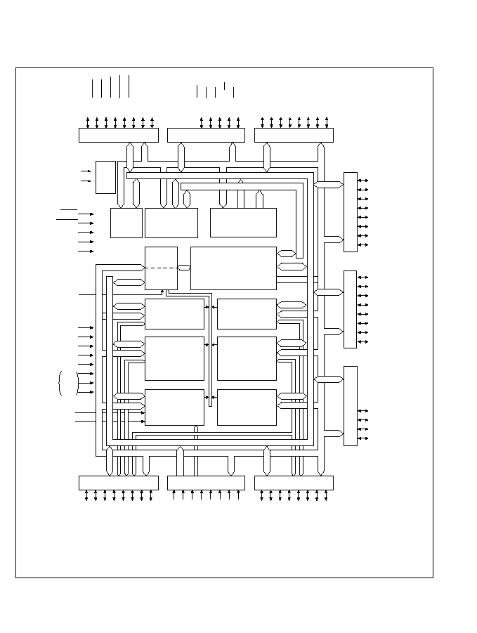
1.2 Block Diagram
Figure 1-1 shows a block diagram of the H8/532 chip.
CPU
P4 /A
7
7
P4 /A
6
6
P4 /A
5
5
P4 /A
4
4
P4 /A
3
3
P4 /A
2
2
P4 /A
1
1
P4 /A
0
0
P5 /A
15
7
P5 /A
14
6
P5 /A
13
5
P5 /A
12
4
P5 /A
11
3
P5 /A
10
2
P5 /A
9
1
P5 /A
8
0
P6 /A
19
3
P6 /A
18
2
P6 /A
17
1
P6 /A
16
0
P7 /FTOA
1
7
P7 /FTI
2
2
P7 /FTI
1
1
P7 /TMCI
0
P7 /FTOB /FTCI
3
63
P7 /FTOB /FTCI
2
52
P7 /FTOB /FTCI
1
4
P7 /FTI /TMRI
3
3
1
P8 /AN
7
7
P8 /AN
6
6
P8 /AN
5
5
P8 /AN
4
4
P8 /AN
3
3
P8 /AN
2
2
P8 /AN
1
1
P8 /AN
0
0
8 Bits Timer
16 Bits Free
Running Timer
(x 3 channel)
Watchdog
Timer
Serial
Communication
Interface
PWM Timer
(x 3 channel)
10 Bits
A/D Converter
Port 9
Port 8
Port 7
Port 6
Port 5
Port 4
Port 3
Port 2
Port 1
Clock
Gener-
ator
EXTAL
XTAL
Wait-
State
Controller
RAM
1 kByte
PROM/Mask
ROM 32 kByte
Interrupt
Controller
Data
Transfer
Controller
V
cc
V
cc
V
ss
V
ss
V
ss
V
ss
V
ss
V
ss
*
AV
cc
AV
ss
NMI
RES
STBY
MD
0
MD
1
MD
2
P9 /SCK
7
P9 /RXD
6
P9 /TXD
5
P9 /PW
3
4
P9 /PW
2
3
P9 /PW
1
2
P9 /FTOA
3
1
P9 /FTOA
2
0
* CP-84 and CG-84 only
P3 /D
7
7
P3 /D
6
6
P3 /D
5
5
P3 /D
4
4
P3 /D
3
3
P3 /D
2
2
P3 /D
1
1
P3 /D
0
0
P1 /TMO
7
P1 /IRQ
1
6
P1 /IRQ
0
5
P1 /WAIT
4
P1 /BREQ
3
P1 /BACK
2
P1 /E
1
P1 /¯
0
P2 /WR
4
P2 /RD
3
P2 /DS
2
P2 /R/W
1
P2 /AS
0
Data bus (Low)
Data bus (High)
Address bus
4
Figure 1-1 Block Diagram
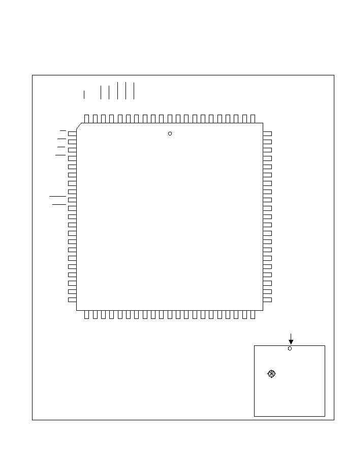
1.3 Pin Arrangements and Functions
1.3.1 Pin Arrangement
Figure 1-2 shows the pin arrangement of the CP-84 package. Figure 1-3 shows the pin
arrangement of the CG-84 package. Figure 1-4 shows the pin arrangement of the FP-80A package.
1 pin
P2 /R/W
P2 /DS
P2 /RD
P2 /WR
V
MD
MD
MD
STBY
RES
NMI
NC
V
P3 /D
P3 /D
P3 /D
P3 /D
P3 /D
P3 /D
P3 /D
P3 /D
1
2
3
4
cc
0
1
2
ss
0
1
2
3
4
5
6
7
0
1
2
3
4
5
6
7
12
13
14
15
16
17
18
19
20
21
22
23
24
25
26
27
28
29
30
31
32
74
73
72
71
70
69
68
67
66
65
64
63
62
61
60
59
58
57
56
55
54
11 10 9
8
7
6
5
4
3
2
1 84 83 82 81 80 79 78 77 76 75
33 34 35 36 37 38 39 40 41 42 43 44 45 46 47 48 49 50 51 52 53
PLCC-84
H8/532
HD6475328CP
JAPAN
AV
P8 /AN
P8 /AN
P8 /AN
P8 /AN
P8 /AN
P8 /AN
P8 /AN
P8 /AN
AV
V
P7 /FTOA
P7 /FTOB /FTCI
P7 /FTOB /FTCI
P7 /FTOB /FTCI
P7 /FTI /TMRI
P7 /FTI
P7 /FTI
P7 /TMCI
V
P6 /A
cc
7
7
6
6
5
5
4
4
3
3
2
2
1
1
0
0
ss
ss
7
6
5
4
3
2
1
0
cc
3
1
3
2
1
3
2
1
3
2
1
19
P2 /AS
P1 /TMO
P1 /IRQ
P1 /IRQ
P1 /WAIT
P1 /BREQ
P1 /BACK
P1 /E
P1 /¯
V
XTAL
EXTAL
V
P9 /SCK
P9 /RXD
P9 /TXD
P9 /PW
P9 /PW
P9 /PW
P9 /FTOA
P9 /FTOA
0
7
6
5
4
3
2
1
0
ss
ss
7
6
5
4
3
2
1
0
3
2
1
3
2
1
0
P4 /A
P4 /A
P4 /A
P4 /A
P4 /A
P4 /A
P4 /A
P4 /A
V
V
P5 /A
P5 /A
P5 /A
P5 /A
P5 /A
P5 /A
P5 /A
P5 /A
P6 /A
P6 /A
P6 /A
0
1
2
3
4
5
6
7
ss
ss
08
19
21
0
31
1
41
2
51
3
61
4
71
5
01
3
11
4
21
5
0
1
2
3
4
5
6
7
5
Figure 1-2 Pin Arrangement (CP-84, Top View)

Index
LCC-84
H8/532
HD6475328CG
JAPAN
P2 /R/W
P2 /DS
P2 /RD
P2 /WR
V
MD
MD
MD
STBY
RES
NMI
NC
V
P3 /D
P3 /D
P3 /D
P3 /D
P3 /D
P3 /D
P3 /D
P3 /D
1
2
3
4
cc
0
1
2
ss
0
1
2
3
4
5
6
7
0
1
2
3
4
5
6
7
12
13
14
15
16
17
18
19
20
21
22
23
24
25
26
27
28
29
30
31
32
74
73
72
71
70
69
68
67
66
65
64
63
62
61
60
59
58
57
56
55
54
11 10 9
8
7
6
5
4
3
2
1 84 83 82 81 80 79 78 77 76 75
33 34 35 36 37 38 39 40 41 42 43 44 45 46 47 48 49 50 51 52 53
AV
P8 /AN
P8 /AN
P8 /AN
P8 /AN
P8 /AN
P8 /AN
P8 /AN
P8 /AN
AV
V
P7 /FTOA
P7 /FTOB /FTCI
P7 /FTOB /FTCI
P7 /FTOB /FTCI
P7 /FTI /TMRI
P7 /FTI
P7 /FTI
P7 /TMCI
V
P6 /A
cc
7
7
6
6
5
5
4
4
3
3
2
2
1
1
0
0
ss
ss
7
6
5
4
3
2
1
0
cc
3
1
3
2
1
3
2
1
3
2
1
19
P2 /AS
P1 /TMO
P1 /IRQ
P1 /IRQ
P1 /WAIT
P1 /BREQ
P1 /BACK
P1 /E
P1 /¯
V
XTAL
EXTAL
V
P9 /SCK
P9 /RXD
P9 /TXD
P9 /PW
P9 /PW
P9 /PW
P9 /FTOA
P9 /FTOA
0
7
6
5
4
3
2
1
0
ss
ss
7
6
5
4
3
2
1
0
3
2
1
3
2
1
0
P4 /A
P4 /A
P4 /A
P4 /A
P4 /A
P4 /A
P4 /A
P4 /A
V
V
P5 /A
P5 /A
P5 /A
P5 /A
P5 /A
P5 /A
P5 /A
P5 /A
P6 /A
P6 /A
P6 /A
0
1
2
3
4
5
6
7
ss
ss
08
19
21
0
31
1
41
2
51
3
61
4
71
5
01
6
11
7
21
8
0
1
2
3
4
5
6
7
Figure 1-3 Pin Arrangement (CG-84, Top View)
6
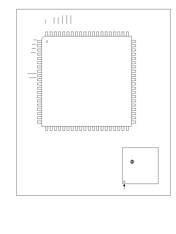
P2 /R/W
P2 /DS
P2 /RD
P2 /WR
V
MD
MD
MD
STBY
RES
NMI
V
P3 /D
P3 /D
P3 /D
P3 /D
P3 /D
P3 /D
P3 /D
P3 /D
1
2
3
4
cc
0
1
2
ss
0
1
2
3
4
5
6
7
0
1
2
3
4
5
6
7
1
2
3
4
5
6
7
8
9
10
11
12
13
14
15
16
17
18
19
20
60
59
58
57
56
55
54
53
52
51
50
49
48
47
46
45
44
43
42
41
80 79 78 77 76 75 74 73 72 71 70 69 68 67 66 65 64 63 62 61
21 22 23 24 25 26 27 28 29 30 31 32 33 34 35 36 37 38 39 40
QFP-80A
H8/532
HD6475328F
JAPAN
AV
P8 /AN
P8 /AN
P8 /AN
P8 /AN
P8 /AN
P8 /AN
P8 /AN
P8 /AN
AV
P7 /FTOA
P7 /FTOB /FTCI
P7 /FTOB /FTCI
P7 /FTOB /FTCI
P7 /FTI /TMRI
P7 /FTI
P7 /FTI
P7 /TMCI
V
P6 /A
cc
7
7
6
6
5
5
4
4
3
3
2
2
1
1
0
0
ss
7
6
5
4
3
2
1
0
cc
3
1
3
2
1
3
2
1
3
2
1
19
P2 /AS
P1 /TMO
P1 /IRQ
P1 /IRQ
P1 /WAIT
P1 /BREQ
P1 /BACK
P1 /E
P1 /¯
V
XTAL
EXTAL
P9 /SCK
P9 /RXD
P9 /TXD
P9 /PW
P9 /PW
P9 /PW
P9 /FTOA
P9 /FTOA
0
7
6
5
4
3
2
1
0
ss
7
6
5
4
3
2
1
0
3
2
1
3
2
1
0
P4 /A
P4 /A
P4 /A
P4 /A
P4 /A
P4 /A
P4 /A
P4 /A
V
P5 /A
P5 /A
P5 /A
P5 /A
P5 /A
P5 /A
P5 /A
P5 /A
P6 /A
P6 /A
P6 /A
0
1
2
3
4
5
6
7
ss
08
19
21
0
31
1
41
2
51
3
61
4
71
5
01
6
11
7
21
8
0
1
2
3
4
5
6
7
1 pin
Figure 1-4 Pin Arrangement (FP-80A, Top View)
7

1.3.2 Pin Functions
Pin Arrangements in Each Operating Mode: Table 1-2 lists the arrangements of the pins of the
CP-84 and CG-84 packages in each operating mode. Table 1-3 lists the arrangements for the FP-
80A package.
Table 1-2 Pin Arrangements in Each Operating Mode (CP-84, CG-84)
Notes: 1. For the PROM mode, see section 17, "ROM."
2. Pins marked NC should be left unconnected.
Pin Name
Expanded Minimum
Expanded Maximum
Single-Chip
PROM
Pin
Modes
Modes
Mode
Mode
No.
Mode 1
Mode 2
Mode 3
Mode 4
Mode 7
1
XTAL
XTAL
XTAL
XTAL
XTAL
NC
2
V
SS
V
SS
V
SS
V
SS
V
SS
V
SS
3
P1
0
/¯ P1
0
/¯ P1
0
/¯ P1
0
/¯ P1
0
/¯ NC
4
P1
1
/E
P1
1
/E
P1
1
/E
P1
1
/E
P1
1
/E
NC
5
P1
2
/ BACK
P1
2
/ BACK
P1
2
/ BACK
P1
2
/ BACK
P1
2
NC
6 P1
3
/ BREQ
P1
3
/ BREQ
P1
3
/ BREQ
P1
3
/ BREQ
P1
3
NC
7
P1
4
/ WAIT
P1
4
/ WAIT
P1
4
/ WAIT
P1
4
/ WAIT
P1
4
NC
8
P1
5
/ IRQ
0
P1
5
/ IRQ
0
P1
5
/ IRQ
0
P1
5
/ IRQ
0
P1
5
/ IRQ
0
NC
9
P1
6
/ IRQ
1
P1
6
/ IRQ
1
P1
6
/ IRQ
1
P1
6
/ IRQ
1
P1
6
/ IRQ
1
NC
10
P1
7
/ TMO
P1
7
/ TMO
P1
7
/ TMO
P1
7
/ TMO
P1
7
/ TMO
NC
11
AS
AS
AS
AS
P2
0
NC
12
R/W
R/W
R/W
R/W
P2
1
NC
13
DS
DS
DS
DS
P2
2
NC
14
RD
RD
RD
RD
P2
3
NC
15
WR
WR
WR
WR
P2
4
NC
16
V
CC
V
CC
V
CC
V
CC
V
CC
V
CC
17
MD
0
MD
0
MD
0
MD
0
MD
0
V
SS
18
MD
1
MD
1
MD
1
MD
1
MD
1
V
SS
8

Table 1-2 Pin Arrangements in Each Operating Mode (CP-84, CG-84) (cont)
Notes: 1. For the PROM mode, see section 17, "ROM."
2. Pins marked NC should be left unconnected.
Pin Name
Expanded Minimum
Expanded Maximum
Single-Chip
PROM
Pin
Modes
Modes
Mode
No.
Mode 1
Mode 2
Mode 3
Mode 4
Mode 7
Mode
19
MD
2
MD
2
MD
2
MD
2
MD
2
V
SS
20
STBY
STBY
STBY
STBY
STBY
V
SS
21
RES
RES
RES
RES
RES
V
PP
22
NMI
NMI
NMI
NMI
NMI
A
9
23
NC
NC
NC
NC
NC
NC
24
V
SS
V
SS
V
SS
V
SS
V
SS
V
SS
25
D
0
D
0
D
0
D
0
P3
0
O
0
26
D
1
D
1
D
1
D
1
P3
1
O
1
27
D
2
D
2
D
2
D
2
P3
2
O
2
28
D
3
D
3
D
3
D
3
P3
3
O
3
29
D
4
D
4
D
4
D
4
P3
4
O
4
30
D
5
D
5
D
5
D
5
P3
5
O
5
31
D
6
D
6
D
6
D
6
P3
6
O
6
32
D
7
D
7
D
7
D
7
P3
7
O
7
33
A
0
A
0
A
0
A
0
P4
0
A
0
34
A
1
A
1
A
1
A
1
P4
1
A
1
35
A
2
A
2
A
2
A
2
P4
2
A
2
36
A
3
A
3
A
3
A
3
P4
3
A
3
37
A
4
A
4
A
4
A
4
P4
4
A
4
38
A
5
A
5
A
5
A
5
P4
5
A
5
39
A
6
A
6
A
6
A
6
P4
6
A
6
40
A
7
A
7
A
7
A
7
P4
7
A
7
41
V
SS
V
SS
V
SS
V
SS
V
SS
V
SS
9

Table 1-2 Pin Arrangements in Each Operating Mode (CP-84, CG-84) (cont)
Notes: 1. For the PROM mode, see section 17, "ROM."
2. Pins marked NC should be left unconnected.
Pin Name
Expanded Minimum
Expanded Maximum
Single-Chip
PROM
Pin
Modes
Modes
Mode
No.
Mode 1
Mode 2
Mode 3
Mode 4
Mode 7
Mode
42
V
SS
V
SS
V
SS
V
SS
V
SS
V
SS
43
A
8
P5
0
/ A
8
A
8
P5
0
/ A
8
P5
0
A
8
44
A
9
P5
1
/ A
9
A
9
P5
1
/ A
9
P5
1
OE
45
A
10
P5
2
/ A
10
A
10
P5
2
/ A
10
P5
2
A
10
46
A
11
P5
3
/ A
11
A
11
P5
3
/ A
11
P5
3
A
11
47
A
12
P5
4
/ A
12
A
12
P5
4
/ A
12
P5
4
A
12
48
A
13
P5
5
/ A
13
A
13
P5
5
/ A
13
P5
5
A
13
49
A
14
P5
6
/ A
14
A
14
P5
6
/ A
14
P5
6
A
14
50
A
15
P5
7
/ A
15
A
15
P5
7
/ A
15
P5
7
CE
51
P6
0
P6
0
A
16
P6
0
/ A
16
P6
0
V
CC
52
P6
1
P6
1
A
17
P6
1
/ A
17
P6
1
V
CC
53
P6
2
P6
2
A
18
P6
2
/ A
18
P6
2
NC
54
P6
3
P6
3
A
19
P6
3
/ A
19
P6
3
NC
55
V
CC
V
CC
V
CC
V
CC
V
CC
V
CC
56
P7
0
/ TMCI
P7
0
/ TMCI
P7
0
/ TMCI
P7
0
/ TMCI
P7
0
/ TMCI
NC
57
P7
1
/ FTI
1
P7
1
/ FTI
1
P7
1
/ FTI
1
P7
1
/ FTI
1
P7
1
/ FTI
1
NC
58
P7
2
/ FTI
2
P7
2
/ FTI
2
P7
2
/ FTI
2
P7
2
/ FTI
2
P7
2
/ FTI
2
NC
59
P7
3
/ FTI
3
/
P7
3
/ FTI
3
/
P7
3
/ FTI
3
/
P7
3
/ FTI
3
/
P7
3
/ FTI
3
/
NC
TMRI
TMRI
TMRI
TMRI
TMRI
60
P7
4
/ FTOB
1
/
P7
4
/ FTOB
1
/ P7
4
/ FTOB
1
/ P7
4
/ FTOB
1
/ P7
4
/ FTOB
1
/
NC
FTCI
1
FTCI
1
FTCI
1
FTCI
1
FTCI
1
61
P7
5
/ FTOB
2
/
P7
5
/ FTOB
2
/ P7
5
/ FTOB
2
/ P7
5
/ FTOB
2
/ P7
5
/ FTOB
2
/
NC
FTCI
2
FTCI
2
FTCI
2
FTCI
2
FTCI
2
10

Table 1-2 Pin Arrangements in Each Operating Mode (CP-84, CG-84) (cont)
Notes: 1. For the PROM mode, see section 17, "ROM."
2. Pins marked NC should be left unconnected.
Pin Name
Expanded Minimum
Expanded Maximum
Single-Chip
PROM
Pin
Modes
Modes
Mode
No.
Mode 1
Mode 2
Mode 3
Mode 4
Mode 7
Mode
62
P7
6
/ FTOB
3
/
P7
6
/ FTOB
3
/ P7
6
/ FTOB
3
/ P7
6
/ FTOB
3
/ P7
6
/ FTOB
3
/
NC
FTCI
3
FTCI
3
FTCI
3
FTCI
3
FTCI
3
63
P7
7
/ FTOA
1
P7
7
/ FTOA
1
P7
7
/ FTOA
1
P7
7
/ FTOA
1
P7
7
/ FTOA
1
NC
64
V
SS
V
SS
V
SS
V
SS
V
SS
V
SS
65
AV
SS
AV
SS
AV
SS
AV
SS
AV
SS
V
SS
66
P8
0
/ AN
0
P8
0
/ AN
0
P8
0
/ AN
0
P8
0
/ AN
0
P8
0
/ AN
0
NC
67
P8
1
/ AN
1
P8
1
/ AN
1
P8
1
/ AN
1
P8
1
/ AN
1
P8
1
/ AN
1
NC
68
P8
2
/ AN
2
P8
2
/ AN
2
P8
2
/ AN
2
P8
2
/ AN
2
P8
2
/ AN
2
NC
69
P8
3
/ AN
3
P8
3
/ AN
3
P8
3
/ AN
3
P8
3
/ AN
3
P8
3
/ AN
3
NC
70
P8
4
/ AN
4
P8
4
/ AN
4
P8
4
/ AN
4
P8
4
/ AN
4
P8
4
/ AN
4
NC
71
P8
5
/ AN
5
P8
5
/ AN
5
P8
5
/ AN
5
P8
5
/ AN
5
P8
5
/ AN
5
NC
72
P8
6
/ AN
6
P8
6
/ AN
6
P8
6
/ AN
6
P8
6
/ AN
6
P8
6
/ AN
6
NC
73
P8
7
/ AN
7
P8
7
/ AN
7
P8
7
/ AN
7
P8
7
/ AN
7
P8
7
/ AN
7
NC
74
AV
CC
AV
CC
AV
CC
AV
CC
AV
CC
V
CC
75
P9
0
/ FTOA
2
P9
0
/ FTOA
2
P9
0
/ FTOA
2
P9
0
/ FTOA
2
P9
0
/ FTOA
2
NC
76
P9
1
/ FTOA
3
P9
1
/ FTOA
3
P9
1
/ FTOA
3
P9
1
/ FTOA
3
P9
1
/ FTOA
3
NC
77
P9
2
/ PW
1
P9
2
/ PW
1
P9
2
/ PW
1
P9
2
/ PW
1
P9
2
/ PW
1
NC
78
P9
3
/ PW
2
P9
3
/ PW
2
P9
3
/ PW
2
P9
3
/ PW
2
P9
3
/ PW
2
NC
79
P9
4
/ PW
3
P9
4
/ PW
3
P9
4
/ PW
3
P9
4
/ PW
3
P9
4
/ PW
3
NC
80
P9
5
/ TXD
P9
5
/ TXD
P9
5
/ TXD
P9
5
/ TXD
P9
5
/ TXD
NC
81
P9
6
/ RXD
P9
6
/ RXD
P9
6
/ RXD
P9
6
/ RXD
P9
6
/ RXD
NC
82
P9
7
/ SCK
P9
7
/ SCK
P9
7
/ SCK
P9
7
/ SCK
P9
7
/ SCK
NC
83
V
SS
V
SS
V
SS
V
SS
V
SS
V
SS
84
EXTAL
EXTAL
EXTAL
EXTAL
EXTAL
NC
11

Table 1-3 Pin Arrangements in Each Operating Mode (FP-80A)
Notes: 1. For the PROM mode, see section 17, "ROM."
2. Pins marked NC should be left unconnected.
Pin Name
Expanded Minimum
Expanded Maximum
Single-Chip
PROM
Pin
Modes
Modes
Mode
No.
Mode 1
Mode 2
Mode 3
Mode 4
Mode 7
Mode
1
R/W
R/W
R/W
R/W
P2
1
NC
2
DS
DS
DS
DS
P2
2
NC
3
RD
RD
RD
RD
P2
3
NC
4
WR
WR
WR
WR
P2
4
NC
5
V
CC
V
CC
V
CC
V
CC
V
CC
V
CC
6
MD
0
MD
0
MD
0
MD
0
MD
0
V
SS
7
MD
1
MD
1
MD
1
MD
1
MD
1
V
SS
8
MD
2
MD
2
MD
2
MD
2
MD
2
V
SS
9
STBY
STBY
STBY
STBY
STBY
V
SS
10
RES
RES
RES
RES
RES
V
PP
11
NMI
NMI
NMI
NMI
NMI
A
9
12
V
SS
V
SS
V
SS
V
SS
V
SS
V
SS
13
D
0
D
0
D
0
D
0
P3
0
O
0
14
D
1
D
1
D
1
D
1
P3
1
O
1
15
D
2
D
2
D
2
D
2
P3
2
O
2
16
D
3
D
3
D
3
D
3
P3
3
O
3
17
D
4
D
4
D
4
D
4
P3
4
O
4
18
D
5
D
5
D
5
D
5
P3
5
O
5
19
D
6
D
6
D
6
D
6
P3
6
O
6
20
D
7
D
7
D
7
D
7
P3
7
O
7
21
A
0
A
0
A
0
A
0
P4
0
A
0
12

Table 1-3 Pin Arrangements in Each Operating Mode (FP-80A) (cont)
Notes: 1. For the PROM mode, see section 17, "ROM."
2. Pins marked NC should be left unconnected.
Pin Name
Expanded Minimum
Expanded Maximum
Single-Chip
PROM
Pin
Modes
Modes
Mode
No.
Mode 1
Mode 2
Mode 3
Mode 4
Mode 7
Mode
22
A
1
A
1
A
1
A
1
P4
1
A
1
23
A
2
A
2
A
2
A
2
P4
2
A
2
24
A
3
A
3
A
3
A
3
P4
3
A
3
25
A
4
A
4
A
4
A
4
P4
4
A
4
26
A
5
A
5
A
5
A
5
P4
5
A
5
27
A
6
A
6
A
6
A
6
P4
6
A
6
28
A
7
A
7
A
7
A
7
P4
7
A
7
29
V
SS
V
SS
V
SS
V
SS
V
SS
V
SS
30
A
8
P5
0
/ A
8
A
8
P5
0
/ A
8
P5
0
A
8
31
A
9
P5
1
/ A
9
A
9
P5
1
/ A
9
P5
1
OE
32
A
10
P5
2
/ A
10
A
10
P5
2
/ A
10
P5
2
A
10
33
A
11
P5
3
/ A
11
A
11
P5
3
/ A
11
P5
3
A
11
34
A
12
P5
4
/ A
12
A
12
P5
4
/ A
12
P5
4
A
12
35
A
13
P5
5
/ A
13
A
13
P5
5
/ A
13
P5
5
A
13
36
A
14
P5
6
/ A
14
A
14
P5
6
/ A
14
P5
6
A
14
37
A
15
P5
7
/ A
15
A
15
P5
7
/ A
15
P5
7
CE
38
P6
0
P6
0
A
16
P6
0
/ A
16
P6
0
V
CC
39
P6
1
P6
1
A
17
P6
1
/ A
17
P6
1
V
CC
40
P6
2
P6
2
A
18
P6
2
/ A
18
P6
2
NC
41
P6
3
P6
3
A
19
P6
3
/ A
19
P6
3
NC
42
V
CC
V
CC
V
CC
V
CC
V
CC
V
CC
13

Table 1-3 Pin Arrangements in Each Operating Mode (FP-80A) (cont)
Notes: 1. For the PROM mode, see section 17, "ROM."
2. Pins marked NC should be left unconnected.
Pin Name
Expanded Minimum
Expanded Maximum
Single-Chip
PROM
Pin
Modes
Modes
Mode
No.
Mode 1
Mode 2
Mode 3
Mode 4
Mode 7
Mode
43
P7
0
/ TMCI
P7
0
/ TMCI
P7
0
/ TMCI
P7
0
/ TMCI
P7
0
/ TMCI
NC
44
P7
1
/ FTI
1
P7
1
/ FTI
1
P7
1
/ FTI
1
P7
1
/ FTI
1
P7
1
/ FTI
1
NC
45
P7
2
/ FTI
2
P7
2
/ FTI
2
P7
2
/ FTI
2
P7
2
/ FTI
2
P7
2
/ FTI
2
NC
46
P7
3
/ FTI
3
/
P7
3
/ FTI
3
/
P7
3
/ FTI
3
/
P7
3
/ FTI
3
/
P7
3
/ FTI
3
/
NC
TMRI
TMRI
TMRI
TMRI
TMRI
47
P7
4
/ FTOB
1
/
P7
4
/ FTOB
1
/ P7
4
/ FTOB
1
/ P7
4
/ FTOB
1
/ P7
4
/ FTOB
1
/
NC
FTCI
1
FTCI
1
FTCI
1
FTCI
1
FTCI
1
48
P7
5
/ FTOB
2
/
P7
5
/ FTOB
2
/ P7
5
/ FTOB
2
/ P7
5
/ FTOB
2
/ P7
5
/ FTOB
2
/
NC
FTCI
2
FTCI
2
FTCI
2
FTCI
2
FTCI
2
49
P7
6
/ FTOB
3
/
P7
6
/ FTOB
3
/ P7
6
/ FTOB
3
/ P7
6
/ FTOB
3
/ P7
6
/ FTOB
3
/
NC
FTCI
3
FTCI
3
FTCI
3
FTCI
3
FTCI
3
50
P7
7
/ FTOA
1
P7
7
/ FTOA
1
P7
7
/ FTOA
1
P7
7
/ FTOA
1
P7
7
/ FTOA
1
NC
51
AV
SS
AV
SS
AV
SS
AV
SS
AV
SS
V
SS
52
P8
0
/ AN
0
P8
0
/ AN
0
P8
0
/ AN
0
P8
0
/ AN
0
P8
0
/ AN
0
NC
53
P8
1
/ AN
1
P8
1
/ AN
1
P8
1
/ AN
1
P8
1
/ AN
1
P8
1
/ AN
1
NC
54
P8
2
/ AN
2
P8
2
/ AN
2
P8
2
/ AN
2
P8
2
/ AN
2
P8
2
/ AN
2
NC
55
P8
3
/ AN
3
P8
3
/ AN
3
P8
3
/ AN
3
P8
3
/ AN
3
P8
3
/ AN
3
NC
56
P8
4
/ AN
4
P8
4
/ AN
4
P8
4
/ AN
4
P8
4
/ AN
4
P8
4
/ AN
4
NC
57
P8
5
/ AN
5
P8
5
/ AN
5
P8
5
/ AN
5
P8
5
/ AN
5
P8
5
/ AN
5
NC
58
P8
6
/ AN
6
P8
6
/ AN
6
P8
6
/ AN
6
P8
6
/ AN
6
P8
6
/ AN
6
NC
59
P8
7
/ AN
7
P8
7
/ AN
7
P8
7
/ AN
7
P8
7
/ AN
7
P8
7
/ AN
7
NC
14

Table 1-3 Pin Arrangements in Each Operating Mode (FP-80A) (cont)
Notes: 1. For the PROM mode, see section 17, "ROM."
2. Pins marked NC should be left unconnected.
Pin Name
Expanded Minimum
Expanded Maximum
Single-Chip
PROM
Pin
Modes
Modes
Mode
No.
Mode 1
Mode 2
Mode 3
Mode 4
Mode 7
Mode
60
AV
CC
AV
CC
AV
CC
AV
CC
AV
CC
V
CC
61
P9
0
/ FTOA
2
P9
0
/ FTOA
2
P9
0
/ FTOA
2
P9
0
/ FTOA
2
P9
0
/ FTOA
2
NC
62
P9
1
/ FTOA
3
P9
1
/ FTOA
3
P9
1
/ FTOA
3
P9
1
/ FTOA
3
P9
1
/ FTOA
3
NC
63
P9
2
/ PW
1
P9
2
/ PW
1
P9
2
/ PW
1
P9
2
/ PW
1
P9
2
/ PW
1
NC
64
P9
3
/ PW
2
P9
3
/ PW
2
P9
3
/ PW
2
P9
3
/ PW
2
P9
3
/ PW
2
NC
65
P9
4
/ PW
3
P9
4
/ PW
3
P9
4
/ PW
3
P9
4
/ PW
3
P9
4
/ PW
3
NC
66
P9
5
/ TXD
P9
5
/ TXD
P9
5
/ TXD
P9
5
/ TXD
P9
5
/ TXD
NC
67
P9
6
/ RXD
P9
6
/ RXD
P9
6
/ RXD
P9
6
/ RXD
P9
6
/ RXD
NC
68
P9
7
/ SCK
P9
7
/ SCK
P9
7
/ SCK
P9
7
/ SCK
P9
7
/ SCK
NC
69
EXTAL
EXTAL
EXTAL
EXTAL
EXTAL
NC
70
XTAL
XTAL
XTAL
XTAL
XTAL
NC
71
V
SS
V
SS
V
SS
V
SS
V
SS
V
SS
72
P1
0
/ ¯
P1
0
/ ¯
P1
0
/ ¯
P1
0
/ ¯
P1
0
/ ¯
NC
73
P1
1
/ E
P1
1
/ E
P1
1
/ E
P1
1
/ E
P1
1
/ E
NC
74
P1
2
/ BACK
P1
2
/ BACK
P1
2
/ BACK
P1
2
/ BACK
P1
2
NC
75 P1
3
/ BREQ
P1
3
/ BREQ
P1
3
/ BREQ
P1
3
/ BREQ
P1
3
NC
76
P1
4
/ WAIT
P1
4
/ WAIT
P1
4
/ WAIT
P1
4
/ WAIT
P1
4
NC
77
P1
5
/ IRQ
0
P1
5
/ IRQ
0
P1
5
/ IRQ
0
P1
5
/ IRQ
0
P1
5
/ IRQ
0
NC
78
P1
6
/ IRQ
1
P1
6
/ IRQ
1
P1
6
/ IRQ
1
P1
6
/ IRQ
1
P1
6
/ IRQ
1
NC
79
P1
7
/ TMO
P1
7
/ TMO
P1
7
/ TMO
P1
7
/ TMO
P1
7
/ TMO
NC
80
AS
AS
AS
AS
P2
0
NC
15

Pin Functions: Table 1-4 gives a concise description of the function of each pin.
Table 1-4 Pin Functions
Pin No.
CP-84,
Type
Symbol
CG-84
FP-80A
I/O
Name and Function
Power
V
CC
16, 55
5, 42
I
Power: Connected to the power supply (+5V).
Connect both V
CC
pins to the system power
supply (+5V). The chip will not operate if either pin
is left unconnected.
V
SS
2, 24
12, 29
I
Ground: Connected to ground (0V).
41, 42
71
Connect all V
SS
pins to the system power
64, 83
supply (0V). The chip will not operate if any V
SS
pin is left unconnected.
Clock
XTAL
1
70
I
Crystal: Connected to a crystal oscillator.
The crystal frequency should be double the desired
¯ clock frequency.
If an external clock is input at the EXTAL pin, leave
the XTAL pin unconnected.
EXTAL
84
69
I
External Crystal: Connected to a crystal
oscillator or external clock. The frequency of the
external clock should be double the desired ¯ clock
frequency. See section 8.2, "Oscillator Circuit" for
examples of connections to a crystal and external
clock.
¯ 3
72
O
System Clock: Supplies the ¯ clock to peripheral
devices.
E
4
73
O
Enable Clock: Supplies an E clock to E clock based
peripheral devices.
System
BACK
5
74
O
Bus Request Acknowledge: Indicates
control
that the bus right has been granted to an external
device. Notifies an external device that issued a
BREQ signal that it now has control of the bus.
16

Table 1-4 Pin Functions (cont)
Pin No.
CP-84,
Type
Symbol
CG-84
FP-80A
I/O
Name and Function
System
BREQ
6
75
I
Bus Request: Sent by an external device to the
control
H8/532 chip to request the bus right.
STBY
20
9
I
Standby: A transition to the hardware standby
mode (a power-down state) occurs when a Low
input is received at the STBY pin.
RES
21
10
I
Reset: A Low input causes the H8/532 chip to
reset.
Address A
19
≠ A
0
54 ≠ 43 41 ≠ 30
O
Address Bus: Address output pins.
bus
40 ≠ 33 28 ≠ 21
Data bus D
7
≠ D
0
32 ≠ 25 20 ≠ 13
I/O
Data Bus: 8-Bit bidirectional data bus.
Bus
WAIT
7
76
I
Wait: Requests the CPU to insert one or more Tw
control
states when accessing an off-chip address.
AS
11
80
O
Address Strobe: Goes Low to indicate that there
is a valid address on the address bus.
R/W
12
1
O
Read/Write: Indicates whether the CPU is reading
or writing data on the bus.
∑ High--Read
∑ Low--Write
DS
13
2
O
Data Strobe: Goes Low to indicate the presence of
valid data on the data bus.
RD
14
3
O
Read: Goes Low to indicate that the CPU is reading
an external address.
WR
15
4
O
Write: Goes Low to indicate that the CPU is
writing to an external address.
17

Table 1-4 Pin Functions (cont)
Pin No.
CP-84,
Type
Symbol CG-84 FP-80A
I/O
Name and Function
Interrupt
NMI
22
11
I
NonMaskable Interrupt: Highest-signals priority
interrupt request. The port 1 control register (P1CR)
determines whether the interrupt is requested on the
rising or falling edge of the NMI input.
IRQ
0
8
77
I
Interrupt Request 0 and 1: Maskable interrupt
IRQ
1
9
78
request pins.
Operating MD
2
19
8
I
Mode: Input pins for setting the MCU operating
mode
MD
1
18
7
mode according to the table below.
control
MD
0
17
6
MD
2
MD
1
MD
0
Mode
Description
0
0
0
Mode 0 --
0
0
1
Mode 1 Expanded minimum mode
(ROM disabled)
0
1
0
Mode 2 Expanded minimum mode
(ROM enabled)
0
1
1
Mode 3 Expanded maximum mode
(ROM disabled)
1
0
0
Mode 4 Expanded maximum mode
(ROM enabled)
1
0
1
Mode 5 --
1
1
0
Mode 6 --
1
1
1
Mode 7 Single-chip mode
The inputs at these pins are latched in mode select
bits 2 to 0 (MDS2 ≠ MDS0) of the mode control
register (MDCR) on the rising edge of the RES
signal.
18

Table 1-4 Pin Functions (cont)
Pin No.
CP-84,
Type
Symbol
CG-84
FP-80A I/O
Name and Function
16-Bit free-
FTOA
1
63
50
O
FRT Output Compare A (channels 1, 2, and 3):
running
FTOA
2
75
61
Output pins for the output compare A function
timer (FRT) FTOA
3
76
62
of the free-running timer channels 1, 2, and 3.
FTOB
1
60
47
O
FRT Output Compare B (channels 1, 2, and 3):
FTOB
2
61
48
Output pins for the output compare B function
FTOB
3
62
49
of the free-running timer channels 1, 2, and 3.
FTCI
1
60
47
I
FRT Counter Clock Input (channels 1, 2, and 3):
FTCI
2
61
48
External clock input pins for the free-running
FTCI
3
62
49
counters (FRCs) of free-running timer channels 1,
2, and 3.
FTI
1
57
44
I
FRT Input Capture (channels 1, 2, and 3):
FTI
2
58
45
Input capture pins for free-running timer
FTI
3
59
46
channels 1, 2, and 3.
8-Bit
TMO
10
79
O
8-bit Timer Output: Compare-match output pin
timer
for the 8-bit timer.
TMCI
56
43
I
8-bit Timer Clock Input: External
clock input pin for the 8-bit timer counter.
TMRI
59
46
I
8-bit Timer Counter Reset Input: A high input
at this pin resets the 8-bit timer counter.
PWM
PW
1
77
63
O
PWM Timer Output (channels 1, 2, and 3):
timer
PW
2
78
64
Pulse-width modulation timer output pulses.
PW
3
79
65
19

Table 1-4 Pin Functions (cont)
Pin No.
CP-84,
Type
Symbol
CG-84
FP-80A
I/O
Name and Function
Serial com- TXD
80
66
O
Transmit Data: Data output pins for the
munication
serial communication interface.
interface
signals
RXD
81
67
I
Receive Data: Data input pins for the
serial communication interface.
SCK
82
68
I/O
Serial Clock: Input/output pin for the
serial interface clock.
A/D
AN
7
≠ AN
0
73 ≠ 66
59 ≠ 52
I
Analog Input: Analog signal input pins.
converter
AV
CC
*
74
60
I
Analog Reference Voltage: Reference voltage
and power supply pin for the A/D converter.
AV
SS
*
65
51
I
Analog Ground: Ground pin for the A/D
converter.
Parallel
P1
7
≠ P1
0
10 ≠ 3
79 ≠ 72
I/O
Port 1: An 8-bit input/output port. The
I/O
direction of each bit is determined by the port 1
data direction register (P1DDR).
P2
4
≠ P2
0
15 ≠ 11
4 ≠ 1,
I/O
Port 2: A 5-bit input/output port. The
80
direction of each bit is determined by the port 2
data direction register (P2DDR).
P3
7
≠ P3
0
32 ≠ 25
20 ≠ 13
I/O
Port 3: An 8-bit input/output port. The
direction of each bit is determined by the port 3
data direction register (P3DDR).
P4
7
≠ P4
0
40 ≠ 33
28 ≠ 21
I/O
Port 4: An 8-bit input/output port. The
direction of each bit is determined by the port 4
data direction register (P4DDR). These pins
can drive LED indicators.
*
When A/D converter is not used, AV
CC
should be connected to V
CC
, and AV
SS
should be
connected to GND.
20

Table 1-4 Pin Functions (cont)
Pin No.
CP-84,
Type
Symbol
CG-84
FP-80A I/O
Name and Function
Parallel
P5
7
≠ P5
0
50 ≠ 43 37 ≠ 30 I/O
Port 5: An 8-bit input/output port. The direction of
I/O
each bit is determined by the port 5 data direction
register (P5DDR). These pins have built-in MOS
input pull-ups.
P6
3
≠ P6
0
54 ≠ 51 41 ≠ 38 I/O
Port 6: A 4-bit input/output port. The direction of
each bit is determined by the port 6 data direction
register (P6DDR). These pins have built-in MOS
input pull-ups.
P7
7
≠ P7
0
63 ≠ 56 50 ≠ 43 I/O
Port 7: An 8-bit input/output port. The direction of
each bit is determined by the port 7 data direction
register (P7DDR). These pins have Schmitt inputs.
P8
7
≠ P8
0
73 ≠ 66 59 ≠ 52 I
Port 8: An 8-bit input port
P9
7
≠ P9
0
82 ≠ 75 68 ≠ 61 I/O
Port 9: An 8-bit input/output port. The direction of
each bit is determined by the port 9 data direction
register (P9DDR).
21

Section 2 MCU Operating Modes and Address Space
2.1 Overview
The H8/532 microcomputer unit (MCU) operates in five modes numbered 1, 2, 3, 4, and 7. The
mode is selected by the inputs at the mode pins (MD
2
to MD
0
) at the instant when the chip comes
out of a reset. As indicated in table 2-1, the MCU mode determines the size of the address space,
the usage of on-chip ROM, and the operating mode of the CPU. The MCU mode also affects the
functions of I/O pins.
Table 2-1 Operating Modes
MD
2
MD
1
MD
0
MCU Mode
Address Space
On-Chip ROM
CPU Mode
0
0
0
--
--
--
--
0
0
1
Mode 1
Expanded minimum
Disabled
Minimum mode
0
1
0
Mode 2
Expanded minimum
Enabled
Minimum mode
0
1
1
Mode 3
Expanded maximum
Disabled
Maximum mode
1
0
0
Mode 4
Expanded maximum
Enabled
Maximum mode
1
0
1
--
--
--
--
1
1
0
--
--
--
--
1
1
1
Mode 7
Single-chip only
Enabled
Minimum mode
Notation: 0: Low level
1: High level
--: Cannot be used
Modes 1 to 4 are referred to as "expanded" because they permit access to off-chip memory and
peripheral addresses. The expanded minimum modes (modes 1 and 2) support a maximum
address space of 64K bytes. The expanded maximum modes (modes 3 and 4) support a maximum
address space of 1M byte.
Interrupt service is slightly slower in the expanded maximum modes than in the other modes
because the CPU has to save its code page register.
The H8/532 cannot be set to modes 0, 5, and 6. The mode pins should never be set to these
values.
23

2.2 Mode Descriptions
The five MCU modes are described below. For further information on the I/O pin functions in
each mode, see section 9, "I/O Ports."
Mode 1 (Expanded Minimum Mode): Mode 1 supports a maximum 64K-byte address space
which does not include any on-chip ROM. Ports 1 to 5 are used for bus lines and bus control
signals as follows:
Control signals: Ports 1* and 2
Data bus:
Port 3
Address bus:
Ports 4 and 5
* The functions of individual pins of port 1 are software-selectable.
Mode 2 (Expanded Minimum Mode): Mode 2 supports a maximum 64K-byte address space of
which the first 32K bytes are in on-chip ROM. Ports 1 to 5 are used for bus lines and bus control
signals as follows:
Control signals: Ports 1* and 2
Data bus:
Port 3
Address bus:
Ports 4 and 5*
* The functions of individual pins in ports 1 and 5 are software-selectable.
Note: In mode 2, port 5 is initially a general-purpose input port. Software must change it to
output before using it for the address bus. See section 9.6, "Port 5" for details. The following
instruction makes all pins of port 5 into output pins:
MOV.B #H'FF, @H'FF88*
* H'xx or H'xxxx express the hexadecimal number.
Mode 3 (Expanded Maximum Mode): Mode 3 supports a maximum 1M-byte address space
which does not include any on-chip ROM. Ports 1 to 6 are used for bus lines and bus control
signals as follows:
Control signals: Ports 1* and 2
Data bus:
Port 3
Address bus:
Ports 4, 5, and 6
* The functions of individual pins of port 1 are software-selectable.
24

Mode 4 (Expanded Maximum Mode): Mode 4 supports a maximum 1M-byte address space of
which the first 32K bytes are in on-chip ROM. Ports 1 to 6 are used for bus lines and bus control
signals as follows:
Control signals: Ports 1* and 2
Data bus:
Port 3
Address bus:
Ports 4, 5*, and 6*
* The functions of individual pins in ports 1, 5, and 6 are software-selectable.
Note: In mode 4, ports 5 and 6 are initially general-purpose input ports. Software must change
them to output before using them for the address bus. See section 9.6, "Port 5" and 10.7, "Port 6"
for details. The following instruction sets all pins of ports 5 and 6 to output:
MOV.W #H'FFFF, @H'FF88
Mode 7 (Single-Chip Mode): In this mode all memory is on-chip, in 32K bytes of ROM and 1K
byte of RAM. It is not possible to access off-chip addresses.
The single-chip mode provides the maximum number of ports. All the pins associated with the
address and data buses in the expanded modes are available as general-purpose input/output ports
in the single-chip mode.
2.3 Address Space Map
2.3.1 Page Segmentation
The H8/532's address space is segmented into 64K-byte pages. In the single-chip mode and
expanded minimum modes there is just one page: page 0. In the expanded maximum modes there
can be up to 16 pages. Figure 2-1 shows the address space in each mode and indicates which parts
are on- and off-chip.
25
On-chip
On- or off-chip (selectable)
Off-chip
Address
Mode 1
Mode 2
Mode 3
Mode 4
Mode 7
H'00000
Page 0
H'0FFFF
H'10000
Page 1
H'1FFFF
H'F0000
Page 15
H'FFFFF
Expanded minimum modes
Expanded maximum modes
Single-chip mode
Figure 2-1 Address Space in Each Mode
26

2.3.2 Page 0 Address Allocations
The high and low address areas in page 0 are reserved for registers and vector tables.
Vector Tables: The low address area contains the exception vector table and DTC vector table.
The CPU accesses the exception vector table to obtain the addresses of user-coded exception-
handling routines. The DTC vector table contains pointers to tables of register information used
by the on-chip chip data transfer controller. The size of these tables depends on the CPU
operating mode. Details are given in section 4.1.3, "Exception Factors and Vector Table," section
5.2.3, "Interrupt Vector Table," and section 6.3.2, "DTC Vector Table."
In modes 2 and 4 the vector tables are located in on-chip ROM. In modes 1, 3, and 7 the vector
tables are in external memory.
Register Field: The highest 128 addresses in page 0 (addresses H'FF80 to H'FFFF) belong to
control, status, and data registers used by the I/O ports and on-chip supporting modules. Program
code cannot be located at these addresses.
The CPU accesses addresses in this register field like other addresses in the address space. By
reading and writing at these addresses the CPU controls the on-chip supporting modules and
communicates via the I/O ports. A complete map of the register field is given in appendix B.
On-Chip RAM: One of the control registers in the register field is a RAM control register
(RAMCR) containing a RAM enable bit (RAME) that enables or disables the 1-kbyte on-chip
RAM. When this bit is set to "1" (its default value), addresses H'FFB0 to H'FF7F are located on-
chip. When this bit is cleared to "0," these addresses are located in external memory and the on-
chip RAM is not used. See section 16, "RAM" for further information.
The RAME bit is bit 7 at address H'FFF9.
Coding Example:
To enable on-chip RAM:
BSET.B #7, @H'FFF9
To disable on-chip RAM:
BCLR.B #7, @H'FFF9
Note: If on-chip RAM is disabled in the single-chip mode, access to addresses H'FFB0 to H'FF7F
causes an address error.
27
Figure 2-2 is a map of page 0 of the address space.
On-chip RAM (when enabled)
H'0000
Exception vector table
DTC vector table
H'7FFF
H'8000
H'FB80
H'FF80
H'FFFF
On-chip register field
On-chip ROM
(modes 2, 4, and 7)
or external memory
(modes 1 and 3)
Figure 2-2 Map of Page 0
28

2.4 Mode Control Register (MDCR)
Another control register in the register field in page 0 is the mode control register (MDCR). The
inputs at the mode pins are latched in this register on the rising edge of the signal. The mode
control register can be read by the CPU, but not written. Table 3-2 lists the attributes of this
register.
Table 2-2 Mode Control Register
Name
Abbreviation
Read/Write
Address
Mode control register
MDCR
Read only
H'FFFA
The bit configuration of this register is shown below.
* Initialized according to MD
2
to MD
0
.
Bits 7 and 6--Reserved: These bits cannot be modified and are always read as "1."
Bits 5 to 3--Reserved: These bits cannot be modified and are always read as "0."
Bits 2 to 0--Mode Select 2 to 0 (MDS2 to MDS0): These bits indicate the values of the mode
pins (MD
2
to MD
0
) latched on the rising edge of the signal. MDS2 corresponds to MD
2
, MDS1
to MD
1
, and MDS0 to MD
0
. These bits can be read but not written.
Coding Example: To test whether the MCU is operating in mode 1:
CMP:G.B #H'C1, @H'FFFA
The comparison is with H'C1 instead of H'01 because bits 7 and 6 are always read as "1."
Bit
7
6
5
4
3
2
1
0
--
--
--
--
--
MDS2
MDS1
MDS0
Initial value
1
1
0
0
0
*
*
*
Read/Write
--
--
--
--
--
R
R
R
29

Section 3 CPU
3.1 Overview
The H8/532 chip has the H8/500 Family CPU: a high-speed central processing unit designed for
realtime control of a wide range of medium-scale office and industrial equipment. Its Hitachi-
original architecture features eight 16-bit general registers, internal 16-bit data paths, and an
optimized instruction set.
Section 3 summarizes the CPU architecture and instruction set.
3.1.1 Features
The main features of the H8/500 CPU are listed below.
∑ General-register machine
-- Eight 16-bit general registers
-- Seven control registers (two 16-bit registers, five 8-bit registers)
∑ High speed: maximum 10MHz
At 10MHz a register-register add operation takes only 200ns.
∑ Address space managed in 64k-byte pages, expandable to 1M byte*
Page registers make four pages available simultaneously: a code page, stack page, data page,
and extended page.
∑ Two CPU operating modes:
-- Minimum mode: Maximum 64k-byte address space
-- Maximum mode: Maximum 1M-byte address space*
∑ Highly orthogonal instruction set
Addressing modes and data sizes can be specified independently within each instruction.
∑ 1.5 Addressing modes
Register-register and register-memory operations are supported.
∑ Optimized for efficient programming in C language
In addition to the general registers and orthogonal instruction set, the CPU has special short
formats for frequently-used instructions and addressing modes.
* The CPU architecture supports up to 16M bytes of external memory, but the H8/532 chip has
only enough address pins to address 1M byte.
31

3.1.2 Address Space
The address space size depends on the operating mode.
The H8/532 MCU has five operating modes, which are selected by the input to the mode pins
(MD
2
to MD
0
) when the chip comes out of a reset. The CPU, however, has only two operating
modes. The MCU operating mode determines the CPU operating mode, which in turn determines
the maximum address space size as indicated in figure 3-1.
Minimum mode
CPU operating mode
Maximum mode
Maximum address space: 64 k
bytes Hightest address: H'FFFF
Maximum address space: 1 M byte
Hightest address: H'FFFFF
Figure 3-1 CPU Operating Modes
32
3.1.3 Register Configuration
Figure 3-2 shows the register structure of the CPU. There are two groups of registers: the general
registers (Rn) and control registers (CR).
R 0
R 1
R 2
R 3
R 4
R 5
R 6
R 7
(FP)
(SP)
P C
S R
C C R
15
0
15
8 7
0
T
I2 I1 I0
N Z V C
C P
D P
E P
T P
B R
FP: Frame Pointer
SP: Stack Pointer
PC: Program Counter
SR: Status Register
CCR: Condition Code Register
CP: Code Page register
DP: Data Page register
EP: Extended Page register
TP: sTack Page register
BR: Base Register
General registers (Rn)
Control registers (CR)
15
0
Figure 3-2 Registers in the CPU
33
3.2 CPU Register Descriptions
3.2.1 General Registers
All eight of the 16-bit general registers are functionally alike; there is no distinction between data
registers and address registers. When these registers are accessed as data registers, either byte or
word size can be selected.
R6 and R7, in addition to functioning as general registers, have special assignments.
R7 is the stack pointer, used implicitly in exception handling and subroutine calls. It can be
designated by the name SP, which is synonymous with R7. As indicated in figure 3-3, it points to
the top of the stack. It is also used implicitly by the LDM and STM instructions, which load and
store multiple registers from and to the stack and pre-decrement or post-increment R7 accordingly.
R6 functions as a frame pointer (FP). The LINK and UNLK use R6 implicitly to reserve or
release a stack frame.
SP
Unused area
Stack area
Figure 3-3 Stack Pointer
34

3.2.2 Control Registers
The CPU control registers (CR) include a 16-bit program counter (PC), a 16-bit status register
(SR), four 8-bit page registers, and one 8-bit base register (BR).
Program Counter (PC): This 16-bit register indicates the address of the next instruction the
CPU will execute.
Status Register (SR): This 16-bit register contains internal status information. The lower half of
the status register is referred to as the condition code register (CCR): it can be accessed as a
separate condition code byte.
Bit 15--Trace (T): When this bit is set to "1," the CPU operates in trace mode and generates a
trace exception after every instruction. See section 4.4, "Trace" for a description of the trace
exception-handling sequence.
When the value of this bit is "0," instructions are executed in normal continuous sequence. This
bit is cleared to "0" at a reset.
Bits 14 to 11--Reserved: These bits cannot be modified and are always read as "0."
Bits 10 to 8--Interrupt Mask (I2, I1, I0): These bits indicate the interrupt request mask level
(0 to 7). As shown in table 3-1, an interrupt request is not accepted unless it has a higher level
than the value of the mask. A nonmaskable interrupt (NMI), which has level 8, is accepted at any
mask level. After an interrupt is accepted, I2, I1, and I0 are changed to the level of the interrupt.
Table 3-2 indicates the values of the I bits after an interrupt is accepted.
A reset sets all three of bits (I2, I1, and I0) to "1," masking all interrupts except NMI.
Bit
15
14
13
12
11
10
9
8
7
6
5
4
3
2
1
0
T
--
--
--
--
I2
I1
I0
--
--
--
--
N
Z
V
C
CCR
35

Table 3-1 Interrupt Mask Levels
Mask
Mask Bits
Priority
Level
I2
I1
I0
Interrupts Accepted
High
7
1
1
1
NMI
6
1
1
0
Level 7 and NMI
5
1
0
1
Levels 6 to 7 and NMI
4
1
0
0
Levels 5 to 7 and NMI
3
0
1
1
Levels 4 to 7 and NMI
2
0
1
0
Levels 3 to 7 and NMI
1
0
0
1
Levels 2 to 7 and NMI
Low
0
0
0
0
Levels 1 to 7 and NMI
Table 3-2 Interrupt Mask Bits after an Interrupt is Accepted
Level of Interrupt Accepted
I2
I1
I0
NMI (8)
1
1
1
7
1
1
1
6
1
1
0
5
1
0
1
4
1
0
0
3
0
1
1
2
0
1
0
1
0
0
1
36

Bits 7 to 4--Reserved: These bits cannot be modified and are always read as "0."
Bit 3--Negative (N): This bit indicates the most significant bit (sign bit) of the result of an
instruction.
Bit 2--Zero (Z): This bit is set to "1" to indicate a zero result and cleared to "0" to indicate a
nonzero result.
Bit 1--Overflow (V): This bit is set to "1" when an arithmetic overflow occurs, and cleared to
"0" at other times.
Bit 0--Carry (C): This bit is set to "1" when a carry or borrow occurs at the most significant bit,
and is cleared to "0" (or left unchanged) at other times.
The specific changes that occur in the condition code bits when each instruction is executed are
listed in appendix A.1 "Instruction Tables." See the H8/500 Series Programming Manual for
further details.
Page Registers: The code page register (CP), data page register (DP), extended page register
(EP), and stack page register (TP) are 8-bit registers that are used only in the maximum mode. No
use of their contents is made in the minimum mode.
In the maximum mode, the page registers combine with the program counter and general registers
to generate 24-bit effective addresses as shown in figure 3-4, thereby expanding the program area,
data area, and stack area.
37

Code Page Register (CP): The code page register and the program counter combine to generate
a 24-bit program code address. In the maximum mode, the code page register is initialized at a
reset to a value loaded from the vector table, and both the code page register and program counter
CP
DP
EP
TP
PC
R0
R4
R5
R6
R7
R1
R2
R3
@ aa : 16
Page register
8 Bits
16 Bits
24 Bits (effective address)
PC or general register
Figure 3-4 Combinations of Page Registers with Other Registers
38

are saved and restored in exception handling.
Data Page Register (DP): The data page register combines with general registers R0 to R3 to
generate a 24-bit effective address. The data page register contains the upper 8 bits of the address.
It is used to calculate effective addresses in the register indirect addressing mode using R0 to R3,
and in the 16-bit absolute addressing mode (@aa:16).
The data page register is rewritten by the LDC instruction.
Extended Page Register (EP): The extended page register combines with general register R4 or
R5 to generate a 24-bit operand address. The extended page register contains the upper 8 bits of
the address. It is used to calculate effective addresses in the register indirect addressing mode
using R4 or R5.
The extended page can be used as an additional data page.
Stack Page Register (TP): The stack page register combines with R6 (FP) or R7 (SP) to
generate a 24-bit stack address. The stack page register contains the upper 8 bits of the address. It
is used to calculate effective addresses in the register indirect addressing mode using R6 or R7, in
exception handling, and subroutine calls.
Base Register (BR): This 8-bit register stores the base address used in the short absolute
addressing mode (@aa:8). In this addressing mode a 16-bit effective address in page 0 is
generated by using the contents of the base register as the upper 8 bits and an address given in the
instruction code as the lower 8 bits. See figure 3-5.
In the short absolute addressing mode the address is always located in page 0.
BR
@ aa : 8
8 Bits
8 Bits
16 Bits (effective address)
Figure 3-5 Short Absolute Addressing Mode and Base Register
39

3.2.3 Initial Register Values
When the CPU is reset, its internal registers are initialized as shown in table 3-3. Note that the
stack pointer (R7) and base register (BR) are not initialized to fixed values. Also, of the page
registers used in maximum mode, only the code page register (CP) is initialized; the other three
page registers come out of the reset state with undetermined values.
Accordingly, in the minimum mode the first instruction executed after a reset should initialize the
stack pointer. The base register must also be initialized before the short absolute addressing mode
(@aa:8) is used.
In the maximum mode, the first instruction executed after a reset should initialize the stack page
register (TP) and the next instruction should initialize the stack pointer. Later instructions should
initialize the base register and the other page registers as necessary.
40

Table 3-3 Initial Values of Registers
3.3 Data Formats
The H8/500 can process 1-bit data, 4-bit BCD data, 8-bit (byte) data, 16-bit (word) data, and 32-
bit (longword) data.
∑ Bit manipulation instructions operate on 1-bit data.
∑ Decimal arithmetic instructions operate on 4-bit BCD data.
∑ Almost all instructions operate on byte and word data.
∑ Multiply and divide instructions operate on longword data.
3.3.1 Data Formats in General Registers
Data of all the sizes above can be stored in general registers as shown in table 3-4.
Initial Value
Register
Minimum Mode
Maximum Mode
General registers
15
0
Undetermined
Undetermined
R7 ≠ R0
Control registers
15
0
Loaded from vector table
Loaded from vector table
PC
SR
CCR
15
8 7
0
H'070x
H'070x
T≠ ≠ ≠ ≠ I2I1I0 ≠ ≠ ≠ ≠ NZVC
(x: undetermined)
(x: undetermined)
7
0
CP
Undetermined
Loaded from vector table
7
0
DP
Undetermined
Undetermined
7
0
EP
Undetermined
Undetermined
7
0
TP
Undetermined
Undetermined
7
0
BR
Undetermined
Undetermined
41

Bit data locations are specified by bit number. Bit 15 is the most significant bit. Bit 0 is the least
significant bit. BCD and byte data are stored in the lower 8 bits of a general register. Word data
use all 16 bits of a general register. Longword data use two general registers: the upper 16 bits
are stored in Rn (n must be an even number); the lower 16 bits are stored in Rn+1.
Operations performed on BCD data or byte data do not affect the upper 8 bits of the register.
Table 3-4 General Register Data Formats
*
For longword data n must be even (0, 2, 4, or 6).
3.3.2 Data Formats in Memory
Table 3-5 indicates the data formats in memory.
Instructions that access bit data in memory have byte or word operands. The instruction specifies
a bit number to indicate a specific bit in the operand.
Access to word data in memory must always begin at an even address. Access to word data
starting at an odd address causes an address error. The upper 8 bits of word data are stored in
address n (where n is an even number); the lower 8 bits are stored in address n+1.
Data Type
Register No.
Data Structure
1-Bit
BCD
Byte
Word
Longword
Rn
Rn
Rn
Rn
Rn
*
Rn+1
*
15
0
15
14
13
12
11
10
9
8
7
6
5
4
3
2
1
0
15
8
7
4
3
0
Don't-care
Upper digit
Lower digit
15
8
7
0
Don't-care
MSB
LSB
15
0
MSB
LSB
31
16
MSB
Upper 16 bits
Lower 16 bits
LSB
15
0
42

Table 3-5 Data Formats in Memory
When the stack is accessed in exception processing (to save or restore the program counter, code
page register, or status register), word access is always performed, regardless of the actual data
size. Similarly, when the stack is accessed by an instruction using the pre-decrement or post-
increment register indirect addressing mode specifying R7 (@≠R7 or @R7+), which is the stack
pointer, word access is performed regardless of the operand size specified in the instruction. An
address error will therefore occur if the stack pointer indicates an odd address. Programs should
be coded so that the stack pointer always indicates an even address.
Table 3-6 shows the data formats on the stack.
Data Type
Data Format
1-Bit (in byte
operand data)
1-Bit (in word
operand data)
Byte
Word
7
6
5
4
3
2
1
0
7
15
14
13
12
11
10
9
8
6
5
4
3
2
1
0
MSB
LSB
MSB
LSB
Upper 8 bits
Lower 8 bits
Address n
Even address
Odd address
Address n
Even address
Odd address
7
0
43
Table 3-6 Data Formats on the Stack
3.4 Instructions
3.4.1 Basic Instruction Formats
There are two basic CPU instruction formats: the general format and the special format.
General format: This format consists of an effective address (EA) field, an effective address
extension field, and an operation code (OP) field. The effective address is placed before the
operation code because this results in faster execution of the instruction.
∑ Effective address field:
One byte containing information used to calculate the effective
address of an operand.
∑ Effective address extension:
Zero to two bytes containing a displacement value, immediate
data, or an absolute address. The size of the effective address
extension is specified in the effective address field.
∑ Operation code:
Defines the operation to be carried out on the operand located at
the address calculated from the effective address information.
Some instructions (DADD, DSUB, MOVFPE, MOVTPE) have
an extended format in which the operand code is preceded by a
one-byte prefix code.
Data Type
Data Format
Byte data
on stack
Word data
on stack
MSB
LSB
Upper 8 bits
Lower 8 bits
Even address
Odd address
Even address
Odd address
MSB
LSB
Don't-care
Effective address field
Effective address extension
Operation code
44

∑ (Example of prefix code in DADD instruction)
Special Format: In this format the operation code comes first, followed by the effective address
field and effective address extension. This format is used in branching instructions, system
control instructions, and other instructions that can be executed faster if the operation is specified
before the operand.
∑ Operation code: One or two bytes defining the operation to be performed by the instruction.
∑ Effective address field and effective address extension: Zero to three bytes containing
information used to calculate an effective address.
3.4.2 Addressing Modes
The CPU supports 7 addressing modes: (1) register direct; (2) register indirect; (3) register
indirect with displacement; (4) register indirect with pre-decrement or post-increment; (5)
immediate; (6) absolute; and (7) PC-relative.
Due to the highly orthogonal nature of the instruction set, most instructions having operands can
use any applicable addressing mode from (1) through (6). The PC-relative mode (7) is used by
branching instructions.
In most instructions, the addressing mode is specified in the effective address field. The effective-
address extension, if present, contains a displacement, immediate data, or an absolute address.
Table 3-7 indicates how the addressing mode is specified in the effective address field.
Operation code
Effective address field
Effective address extension
Effective address
Prefix code
Operation code
10100rrr
00000000
10100rrr
45

Table 3-7 Addressing Modes
No.
Addressing Mode
Mnemonic
EA Field
EA Extension
1
Register direct
Rn
1 0 1 0 Sz r r r
None
2
Register indirect
@Rn
1 1 0 1 Sz r r r
None
3
Register indirect
@(d:8,Rn)
1 1 1 0 Sz r r r
Displacement (1 byte)
with displacement
@(d:16,Rn)
1 1 1 1 Sz r r r
Displacement (2 bytes)
4
Register indirect
@≠Rn
1 0 1 1 Sz r r r
with pre-decrement
None
Register indirect
@Rn+
1 1 0 0 Sz r r r
with post-increment
5
Immediate
#xx:8
0 0 0 0 0 1 0 0
Immediate data (1 byte)
#xx:16
0 0 0 0 1 1 0 0
Immediate data (2 bytes)
6
Absolute
*
3
@aa:8
0 0 0 0 Sz 1 0 1
1-Byte absolute address
(offset from BR)
@aa:16
0 0 0 1 Sz 1 0 1
2-Byte absolute address
7
PC-relative
disp
No EA field.
1- or 2-byte displacement
Addressing mode
is specified in the
operation code.
Notes:
*
1 Sz: Specifies the operand size.
When Sz = 0: byte operand
When Sz = 1: word operand
*
2 rrr: Register number field, specifying a general register number.
0 0 0 -- R0
0 0 1 -- R1
0 1 0 -- R2
0 1 1 -- R3
1 0 0 -- R4
1 0 1 -- R5
1 1 0 -- R6
1 1 1 -- R7
*
3 The @aa:8 addressing mode is also referred to as the short absolute addressing mode.
*
1
*
2
46
3.4.3 Effective Address Calculation
Table 3-8 explains how the effective address is calculated in each addressing mode.
Table 3-8 Effective Address Calculation
No.
Addressing Mode Effective Address Calculation
Effective Address
1
Register direct
--
Operand is contents of
Rn
Rn
1010Sz rrr
2
Register indirect
--
23
15
0
@Rn
DP
*
1
Rn
1101Sz rrr
Or TP or EP
*
2
3
Register indirect
8 Bits
with displacement
15
0
23
15
0
@(d:8,Rn)
Rn
DP
*
1
Result
15
0
Or TP or EP
*
2
1110Sz rrr
Displacement with
sign extension
@(d:16,Rn)
16 Bits
1111Sz rrr
15
0
23
15
0
Rn
DP
*
1
Result
15
0
Or TP or EP
*
2
4
Register indirect
15
0
23
15
0
with pre-decrement
Rn
DP
*
1
Result
@≠Rn
Or TP or EP
*2
1011Sz rrr
Register indirect
--
23
15
0
with post-increment
DP
*
1
Rn
@Rn+
Rn is incremented by +1 or +2
1100Sz rrr
after instruction execution.
*
3
*
4
*
5
Or TP or EP
*
2
Rn is decremented by ≠1 or ≠2
before instruction execution.
*
3
*
4
*
5
1 or 2
Displacement
≠
+
+
47

Table 3-8 Effective Address Calculation (cont)
No.
Addressing Mode Effective Address Calculation
Effective Address
5
Absolute address
--
23
15
0
@aa:8
H'00
BR
0000Sz101
EA extension data
@aa:16
--
23
15
0
0001Sz101
DP
EA extension data
6
Immediate
--
Operand is 1-byte EA
#xx:8
extension data.
00000100
#xx:16
--
Operand is 2-byte EA
00001100
extension data.
7
PC-relative
8 Bits
disp:8
15
0
23
15
0
No EA code
PC
CP
*
1
Result
Specified in OP code
15
0
Displacement with
sign extension
disp:16
16 Bits
23
15
0
No EA code
15
0
CP
*
1
Result
Specified in OP code
PC
15
0
Displacement
Notes:
*
1 The page register is ignored in minimum mode.
*
2 The page register used in addressing modes 2, 3, and 4 depends on the general register :
DP for R0, R1, R2, or R3; EP for R4 or R5; TP for R6 or R7.
*
3 Decrement by ≠1 for a byte operand, and by ≠2 for a word operand.
*
4 The pre-decrement or post-increment is always ±2 when R7 is specified, even if the
operand is byte size.
*
5 The drawing below shows what happens when the @-SP and @ SP+ addressing
modes are used to save and restore the stack pointer.
48

SP
Old SP-2 (upper byte)
Old SP-2 (lower byte)
MOV.W SP, @≠SP
MOV.W @SP+.SP
SP
SP
49

3.5 Instruction Set
3.5.1 Overview
The main features of the CPU instruction set are:
∑ A general-register architecture.
∑ Orthogonality. Addressing modes and data sizes can be specified independently in each instruction.
∑ 1.5 addressing modes (supporting register-register and register-memory operations)
∑ Affinity for high-level languages, particularly C, with short formats for frequently-used
instructions and addressing modes.
∑ Standard mnemonics, common throughout the H Series.
The CPU instruction set includes 63 types of instructions, listed by function in table 3-9.
Table 3-9 Instruction Classification
* Bcc is a conditional branch instruction in which cc represents a condition code.
Tables 3-10 to 3-16 give a concise summary of the instructions in each functional category. The
MOV, ADD, and CMP instructions have special short formats, which are listed in table 3-17. For
detailed descriptions of the instructions, refer to the H8/500 Series Programming Manual.
The notation used in tables 3-10 to 3-17 is defined below.
Function
Instructions
Types
Data transfer
MOV, LDM, STM, XCH, SWAP, MOVTPE, MOVFPE
7
Arithmetic operations
ADD, SUB, ADDS, SUBS, ADDX, SUBX, DADD, DSUB,
17
MULXU, DIVXU, CMP, EXTS, EXTU, TST, NEG, CLR,
TAS
Logic operations
AND, OR, XOR, NOT
4
Shift
SHAL, SHAR, SHLL, SHLR, ROTL, ROTR, ROTXL,
8
ROTXR
Bit manipulation
BSET, BCLR, BTST, BNOT
4
Branch
Bcc*, JMP, PJMP, BSR, JSR, PJSR, RTS, PRTD,
11
PRTS, RTD, SCB (/F, /NE, /EQ)
System control
TRAPA, TRAP/VS, RTE, SLEEP, LDC, STC, ANDC,
12
ORC, XORC, NOP, LINK, UNLK
Total
63
50

Operation Notation
Rd
General register (destination)
Rs
General register (source)
Rn
General register
(EAd)
Destination operand
(EAs)
Source operand
CCR
Condition code register
N
N (negative) bit of CCR
Z
Z (zero) bit of CCR
V
V (overflow) bit of CCR
C
C (carry) bit of CCR
CR
Control register
PC
Program counter
CP
Code page register
SP
Stack pointer
FP
Frame pointer
#IMM
Immediate data
disp
Displacement
+
Addition
≠
Subtraction
◊
Multiplication
˜
Division
AND logical
OR logical
Exclusive OR logical
Move
Exchange
¨
Not
51

3.5.2 Data Transfer Instructions
Table 3-10 describes the seven data transfer instructions.
Table 3-10 Data Transfer Instructions
Instruction
Size
*
Function
Data
MOV
(EAs)
(EAd), #IMM
(EAd)
transfer
MOV:G
B/W
Moves data between two general registers, or between
MOV:E
B
a general register and memory, or moves immediate data
MOV:I
W
to a general register or memory.
MOV:F
B/W
MOV:L
B/W
MOV:S
B/W
LDM
W
Stack
Rn (register list)
Pops data from the stack to one or more registers.
STM
W
Rn (register list)
stack
Pushes data from one or more registers onto the stack.
XCH
W
Rs
Rd
Exchanges data between two general registers.
SWAP
B
Rd (upper byte)
Rd (lower byte)
Exchanges the upper and lower bytes in a general register.
MOVTPE
B
Rn
(EAd)
Transfers data from a general register to memory in
synchronization with the E clock.
MOVFPE
B
(EAs)
Rd
Transfers data from memory to a general register in
synchronization with the E clock.
Note: B--byte; W--word
52

3.5.3 Arithmetic Instructions
Table 3-11 describes the 17 arithmetic instructions.
Table 3-11 Arithmetic Instructions
Instruction
Size
Function
Arithmetic
ADD
Rd ± (EAs)
Rd, (EAd) ± #IMM
(EAd)
operations
ADD:G
B/W
Performs addition or subtraction on data in a general
ADD:Q
B/W
register and data in another general register or memory, or
SUB
B/W
on immediate data and data in a general register or memory.
ADDS
B/W
SUBS
B/W
ADDX
B/W
Rd ± (EAs) ± C
Rd
SUBX
B/W
Performs addition or subtraction with carry or borrow on
data in a general register and data in another general
register or memory, or on immediate data and data in a
general register or memory.
DADD
B
(Rd)
10
± (Rs)
10
± C
(Rd)
10
DSUB
B
Performs decimal addition or subtraction on data in two
general registers.
MULXU
B/W
Rd
◊
(EAs)
Rd
Performs 8-bit
◊
8-bit or 16-bit
◊
16-bit unsigned
multiplication on data in a general register and data in
another general register or memory, or on data in a
general register and immediate data.
DIVXU
B/W
Rd ˜ (EAs)
Rd
Performs 16-bit ˜ 8-bit or 32-bit ˜ 16-bit unsigned division
on data in a general register and data in another general
register or memory, or on data in a general register and
immediate data.
CMP
Rn ≠ (EAs), (EAd) ≠ #IMM
CMP:G
B/W
Compares data in a general register with data in another
CMP:E
B
general register or memory, or with immediate data, or
CMP:I
W
compares immediate data with data in memory.
Note: B--byte; W--word
53

Table 3-11 Arithmetic Instructions (cont)
Instruction
Size
Function
Arithmetic
EXTS
B
(<bit 7> of <Rd>)
(<bits 15 to 8> of <Rd>)
operations
Converts byte data in a general register to word data by
extending the sign bit.
EXTU
B
0
(<bits 15 to 8> of <Rd>)
Converts byte data in a general register to word data by
padding with zero bits.
TST
B/W
(EAd) ≠ 0
Compares general register or memory contents with 0.
NEG
B/W
0 ≠ (EAd)
(EAd)
Obtains the two's complement of general register or
memory contents.
CLR
B/W
0
(EAd)
Clears general register or memory contents to 0.
TAS
B
(EAd) -- 0, (1)
2
(<bit 7> of <EAd>)
Tests general register or memory contents, then sets the
most significant bit (bit 7) to "1."
Note: B--byte; W--word
3.5.4 Logic Operations
Table 3-12 lists the four instructions that perform logic operations.
Table 3-12 Logic Operation Instructions
Instruction
Size
Function
Logical
AND
B/W
Rd
(EAs)
Rd
operations
Performs a logical AND operation on a general register
and another general register, memory, or immediate data.
OR
B/W
Rd
(EAs)
Rd
Performs a logical OR operation on a general register and
another general register, memory, or immediate data.
XOR
B/W
Rd
(EAs)
Rd
Performs a logical exclusive OR operation on a general register
and another general register, memory, or immediate data.
NOT
B/W
¨ (EAd)
(EAd)
Obtains the one's complement of general register or memory
contents.
Note: B--byte; W--word
54

3.5.5 Shift Operations
Table 3-13 lists the eight shift instructions.
Table 3-13 Shift Instructions
Instruction
Size
Function
Shift
SHAL
B/W
(EAd) shift
(EAd)
operations
SHAR
B/W
Performs an arithmetic shift operation on general register
or memory contents.
SHLL
B/W
(EAd) shift
(EAd)
SHLR
B/W
Performs a logical shift operation on general register or
memory contents.
ROTL
B/W
(EAd) shift
(EAd)
ROTR
B/W
Rotates general register or memory contents.
ROTXL
B/W
(EAd) rotate through carry
(EAd)
ROTXR
B/W
Rotates general register or memory contents through the
C (carry) bit.
Note: B--byte; W--word
55

3.5.6 Bit Manipulations
Table 3-14 describes the four bit-manipulation instructions.
Table 3-14 Bit-Manipulation Instructions
Instruction
Size
Function
Bit
BSET
B/W
¨ (<bit-No.> of <EAd>)
Z,
manipu-
1
(<bit-No.> of <EAd>)
lations
Tests a specified bit in a general register or memory, then
sets the bit to "1." The bit is specified by a bit number
given in immediate data or a general register.
BCLR
B/W
¨ (<bit-No.> of <EAd>)
Z,
0
(<bit-No.> of <EAd>)
Tests a specified bit in a general register or memory, then
clears the bit to "0." The bit is specified by a bit number
given in immediate data or a general register.
BNOT
B/W
¨ (<bit-No.> of <EAd>)
Z,
(<bit-No.> of <EAd>)
Tests a specified bit in a general register or memory, then
inverts the bit. The bit is specified by a bit number given
in immediate data or a general register.
BTST
B/W
¨ (<bit-No.> of <EAd>)
Z
Tests a specified bit in a general register or memory. The
bit is specified by a bit number given in immediate data or
a general register.
Note: B--byte; W--word
56

3.5.7 Branching Instructions
Table 3-15 describes the 11 branching instructions.
Table 3-15 Branching Instructions
Instruction
Size
Function
Branch
Bcc
--
Branches if condition cc is true.
Mnemonic
Description
Condition
BRA (BT)
Always (true)
True
BRN (BF)
Never (false)
False
BHI
High
C
Z = 0
BLS
Low or Same
C
Z = 1
BCC (BHS)
Carry Clear
C = 0
(High or Same)
BCS (BLO)
Carry Set (Low)
C = 1
BNE
Not Equal
Z = 0
BEQ
Equal
Z = 1
BVC
Overflow Clear
V = 0
BVS
Overflow Set
V = 1
BPL
Plus
N = 0
BMI
Minus
N = 1
BGE
Greater or Equal
N
V = 0
BLT
Less Than
N
V = 1
BGT
Greater Than
Z
(N
V) = 0
BLE
Less or Equal
Z
(N
V) = 1
JMP
--
Branches unconditionally to a specified address in the same page.
PJMP
--
Branches unconditionally to a specified address in a specified page.
BSR
--
Branches to a subroutine at a specified address in the same page.
JSR
--
Branches to a subroutine at a specified address in the same page.
PJSR
--
Branches to a subroutine at a specified address in a specified page.
RTS
--
Returns from a subroutine in the same page.
57

Table 3-15 Branching Instructions (cont)
Instruction
Size
Function
Branch
PRTS
--
Returns from a subroutine in a different page.
RTD
--
Returns from a subroutine in the same page and adjusts
the stack pointer.
PRTD
--
Returns from a subroutine in a different page and adjusts
the stack pointer.
SCB/F
--
Controls a loop using a loop counter and/or a specified
SCB/NE
--
termination condition.
SCB/EQ
--
58

3.5.8 System Control Instructions
Table 3-16 describes the 12 system control instructions.
Table 3-16 System Control Instructions
Instruction
Size
Function
System
TRAPA
--
Generates a trap exception with a specified vector number.
control
TRAP/VS
--
Generates a trap exception if the V bit is set to "1" when
the instruction is executed.
RTE
--
Returns from an exception-handling routine.
LINK
--
FP
@≠SP; SP
FP; SP + #IMM
SP
Creates a stack frame.
UNLK
--
FP
SP; @SP+
FP
Deallocates a stack frame created by the LINK instruction.
SLEEP
--
Causes a transition to the power-down state.
LDC
B/W*
(EAs)
CR
Moves immediate data or general register or memory
contents to a specified control register.
STC
B/W*
CR
(EAd)
Moves control register data to a specified general register
or memory location.
ANDC
B/W*
CR
#IMM
CR
Logically ANDs a control register with immediate data.
ORC
B/W*
CR
#IMM
CR
Logically ORs a control register with immediate data.
XORC
B/W*
CR
#IMM
CR
Logically exclusive-ORs a control register with immediate
data.
NOP
--
PC + 1
PC
No operation. Only increments the program counter.
*
The size depends on the control register.
When using the LDC and STC instructions to stack and unstack the BR, CCR, TP, DP, and EP
control registers in the H8/500 family, note the following point.
H8/500 hardware does not permit byte access to the stack. If the LDC.B or STC.B assembler
mnemonic is coded with the @R7 + (@SP+) or @≠R7 (@≠SP) addressing mode, the stack-
pointer addressing mode takes precedence and hardware automatically performs word access.
59

Specifically, the LDC.B and STC.B instructions are executed as follows.
The following applies only to the stack-pointer addressing modes. In addressing modes that do not
use the stack pointer, byte data access is performed as specified by the assembler mnemonic.
(1)
STC.B EP, @≠SP
When word data access is applied to EP, both EP and DP are accessed. This instruction
stores EP at address SP (old) ≠2, and DP at address SP (old) ≠1.
(2)
LDC.B @SP+, EP
When word data access is applied to EP, both EP and DP are accessed. This instruction
loads EP from address SP (old), and DP from address SP (old) +1, updating the DP value as
well as the EP value.
(3)
STC.B CCR, @≠SP
When word data access is applied to CCR, only CCR is accessed. This instruction stores
identical CCR contents at both address SP (old) ≠2 and address SP (old) ≠1.
EP
a
DP
b
Old SP ≠ 2
Before execution
Old SP ≠ 1
Old SP
New SP
After execution
New SP + 1
New SP + 2
a
b
EP
a
DP
b
Old SP
After execution
Old SP + 1
Old SP + 2
New SP ≠ 2
Before execution
New SP ≠ 1
New SP
a
b
EP
a
DP
b
CCR
a
Old SP ≠ 2
Before execution
Old SP ≠ 1
Old SP
New SP
After execution
New SP + 1
New SP + 2
a
b
60

(4)
LDC.B @SP+, CCR
When word data access is applied to CCR, only CCR is accessed. This instruction loads
CCR from address SP (old) +1. Note that the value in address SP (old) is not loaded.
BR, DP, and TP are accessed in the same way as CCR. When DP is specified, both EP and
DP are accessed, but when CCR, BR, DP, or TP is specified, only the specified register is
accessed.
CCR
Old SP
After execution
Old SP + 1
Old SP + 2
New SP ≠ 2
Before execution
New SP ≠ 1
New SP
a
b
CCR
b
61

3.5.9 Short-Format Instructions
The ADD, CMP, and MOV instructions have special short formats. Table 3-17 lists these short
formats together with the equivalent general formats.
The short formats are a byte shorter than the corresponding general formats, and most of them
execute one state faster.
Table 3-17 Short-Format Instructions and Equivalent General Formats
Short-Format
Execution Equivalent General-
Execution
Instruction
Length
States
*
2
Format Instruction
Length
States
*
2
ADD:Q #xx,Rd
*
1
2
2
ADD:G #xx:8,Rd
3
3
CMP:E #xx:8,Rd
2
2
CMP:G.B #xx:8,Rd
3
3
CMP:I #xx:16,Rd
3
3
CMP:G.W #xx:16,Rd
4
4
MOV:E #xx:8,Rd
2
2
MOV:G.B #xx:8,Rd
3
3
MOV:I #xx:16,Rd
3
3
MOV:G.W #xx:16,Rd
4
4
MOV:L @aa:8,Rd
2
5
MOV:G @aa:8,Rd
3
5
MOV:S Rs,@aa:8
2
5
MOV:G Rs,@aa:8
3
5
MOV:F @(d:8,R6),Rd
2
5
MOV:G @(d:8,R6),Rd
3
5
MOV:F Rs,@(d:8,R6)
2
5
MOV:G Rs,@(d:8,R6)
3
5
Notes:
*
1 The ADD:Q instruction accepts other destination operands in addition to a general
register, but the immediate data value (#xx) is limited to ±1 or ±2.
*
2 Number of execution states for access to on-chip memory.
3.6 Operating Modes
The CPU operates in one of two modes: the minimum mode or the maximum mode.
These modes are selected by the mode pins (MD
2
to MD
0
).
3.6.1 Minimum Mode
The minimum mode supports a maximum address space of 64k bytes. The page registers are
ignored. Instructions that branch across page boundaries (PJMP, PJSR, PRTS, PRTD) are invalid.
62

3.6.2 Maximum Mode
In the maximum mode the page registers are valid, expanding the maximum address space to 1M
byte.
The address space is divided into 64k-byte pages. The pages are separate; it is not possible to
move continuously across a page boundary.
It is possible to move from one page to another with branching instructions (PJMP, PJSR, PRTS,
PRTD). The TRAPA instruction and branches to interrupt-handling routines can also jump across
page boundaries. It is not necessary for a program to be contained in a single 64k-byte page.
When data access crosses a page boundary, the program must rewrite the page register before it
can access the data in the next page.
For further information on the operating modes, see section 2, "MCU Operating Modes and
Address Space."
3.7 Basic Operational Timing
3.7.1 Overview
The CPU operates on a system clock (¯) which is created by dividing an oscillator frequency
(fosc) by two. One period of the system clock is referred to as a "state." The CPU accesses
memory in a cycle consisting of 2 or 3 states. The CPU uses different methods to access on-chip
memory, the on-chip register field, and external devices.
Access to On-Chip Memory (RAM, ROM): For maximum speed, access to on-chip memory
(RAM, ROM) is performed in two states, using a 16-bit-wide data bus.
Figure 3-6 shows the on-chip memory access cycle. Figure 3-7 indicates the pin states. The bus
control signals output from the H8/532 chip go to the nonactive state during the access.
Access to On-Chip Register Field (Addresses H'FF80 to H'FFFF): The access cycle consists
of three states. The data bus is 8 bits wide.
Figure 3-8 shows the on-chip supporting module access cycle. Figure 3-9 indicates the pin states.
63
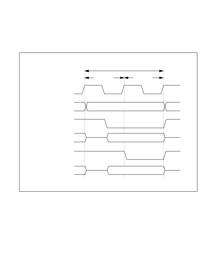
Access to External Devices: The access cycle consists of three states. The data bus is 8 bits
wide. Figure 3-10 (a) and (b) shows the external access cycle. Additional wait states (Tw) can be
inserted by the wait-state controller (WSC).
3.7.2 On-Chip Memory Access Cycle
T state
Memory cycle
1
T state
2
¯
Internal address bus
Internal Read signal
Internal data bus
(Read access)
Internal Write signal
Read data
Address
Write data
Internal data bus
(Write access)
Figure 3-6 On-Chip Memory Access Timing
64
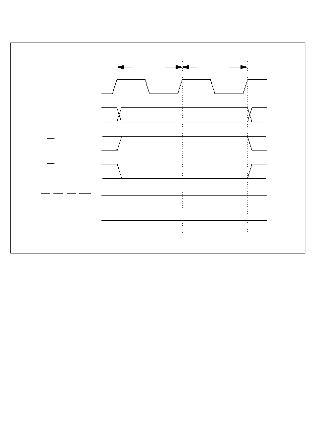
3.7.3 Pin States during On-Chip Memory Access
T state
1
T state
2
¯
A to A
R/W (write access)
19
0
AS, DS, RD, WR
D to D
7
0
R/W (read access)
"High"
High-impedance
Figure 3-7 Pin States during Access to On-Chip Memory
65

3.7.4 Register Field Access Cycle (Addresses H'FF80 to H'FFFF)
T state
Memory cycle
1
T state
2
T state
3
Address
Read data
¯
Internal address bus
Internal Read signal
Internal Write signal
Internal data bus
(write access)
Internal data bus
(read access)
Write data
Figure 3-8 Register Field Access Timing
66
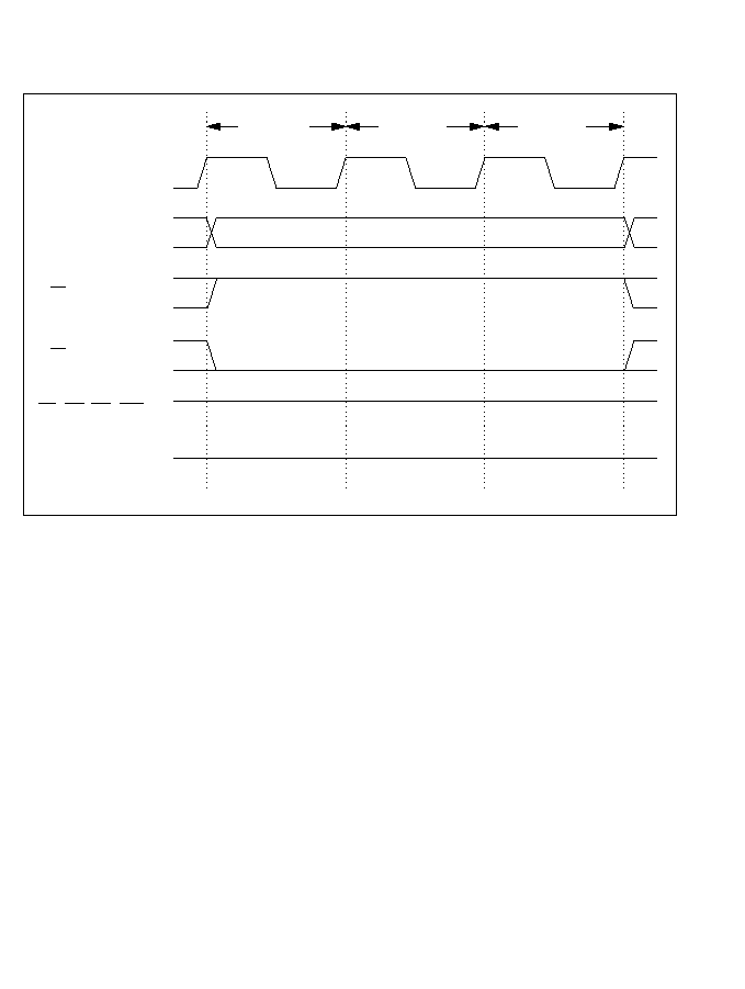
3.7.5 Pin States during Register Field Access (Addresses H'FF80 to H'FFFF)
T state
1
T state
2
T state
3
"High"
¯
A to A
R/W (read access)
19
0
AS, DS, RD, WR
D to D
7
0
R/W (write access)
High-impedance
Figure 3-9 Pin States during Register Field Access
67
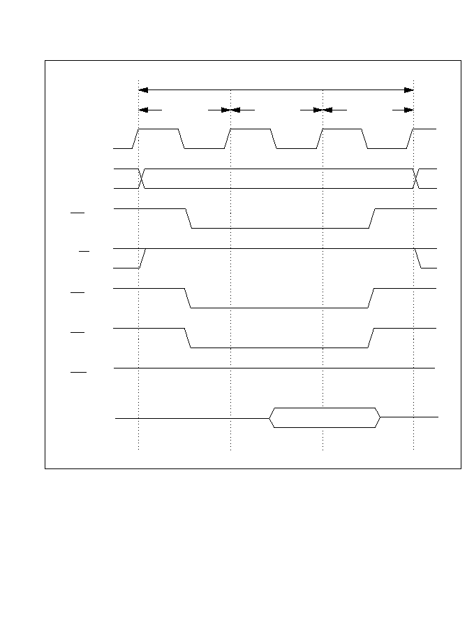
3.7.6 External Access Cycle
Read cycle
T state
1
T state
2
T state
3
Address
R/W
D ≠D
7
0
A ≠A
19
0
¯
AS
WR
DS
RD
"High"
Read data
Figure 3-10 (a) External Access Cycle (Read Access)
68
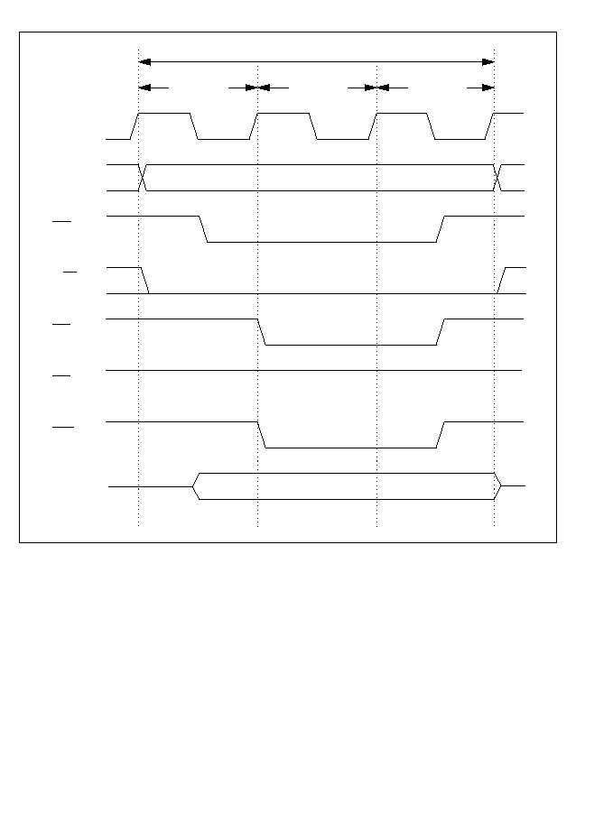
3.8 CPU States
3.8.1 Overview
The CPU has five states: the program execution state, exception-handling state, bus-released state,
reset state, and power-down state. The power-down state is further divided into the sleep mode,
software standby mode, and hardware standby mode. Figure 3-11 summarizes these states, and
figure 3-12 shows a map of the state transitions.
Write cycle
T state
1
T state
2
T state
3
Address
Write data
"High"
R/W
D ≠D
7
0
A ≠A
19
0
¯
AS
WR
DS
RD
Figure 3-10 (b) External Access Cycle (Write Access)
69
State
Program execution state
Exception-handling state
Bus-released state
Reset state
Power-down state
The CPU executes program instructions in sequence.
A transient state in which the CPU executes a hardware
sequence (saving the program counter and status register,
fetching a vector from the vector table, etc.) triggered by a reset,
interrupt, or other exception.
The state in which the CPU has released the external bus in
response to a bus request signal from an external device, and
is waiting for the bus to be returned.
The state in which the CPU and all on-chip supporting
modules have been initialized and are stopped.
A state in which some
or all of the clock
signals are stopped to
conserve power.
Sleep mode
Software standby mode
Hardware standby mode
Figure 3-11 Operating States
70
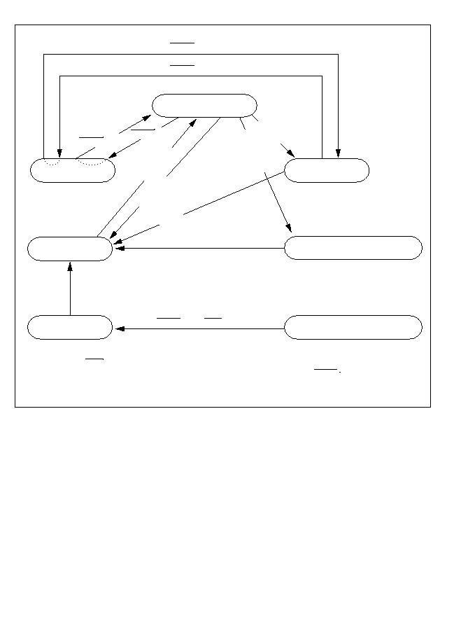
3.8.2 Program Execution State
In this state the CPU executes program instructions in normal sequence.
3.8.3 Exception-Handling State
The exception-handling state is a transient state that occurs when the CPU alters the normal
program flow due to an interrupt, trap instruction, address error, or other exception. In this state
the CPU carries out a hardware-controlled sequence that prepares it to execute a user-coded
exception-handling routine.
BREQ = "0"
BREQ = "0"
BREQ = "1"
Bus-released state
End of
exception
handling
Request
for exception
handling
SLEEP
instruction
with standby
flag set
SLEEP
instruction
Interrupt request
NMI
Program execution state
Exception-handling
state
Sleep mode
Software standby mode
Hardware standby mode
Reset state
*
STBY = "1", RES = "0"
RES = "1"
*
From any state except the hardware standby mode, a transition to the reset state occurs
whenever RES goes Low.
*
A transition to the hardware standby mode from any state occurs when STBY goes Low.
BREQ = "1"
1
*
2
1
2
Figure 3-12 State Transitions
71

In the hardware exception-handling sequence the CPU does the following:
1. Saves the program counter and status register (in minimum mode) or program counter, code
page register, and status register (in maximum mode) to the stack.
2. Clears the T bit in the status register to "0."
3. Fetches the start address of the exception-handling routine from the exception vector table.
4. Branches to that address, returning to the program execution state.
See section 4, "Exception Handling," for further information on the exception-handling state.
3.8.4 Bus-Released State
When so requested, the CPU can grant control of the external bus to an external device. While an
external device has the bus right, the CPU is said to be in the bus-released state. The bus right is
controlled by two pins:
∑ BREQ:
Input pin for the Bus Request signal from an external device
∑ BACK:
Output pin for the Bus Request Acknowledge signal from the CPU, indicating that the
CPU has released the bus
The procedure by which the CPU enters and leaves the bus-released state is:
1. The CPU receives a Low BREQ signal from an external device.
2. The CPU places the address bus pins (A
19
≠ A
0
), data bus pins (D
7
≠ D
0
) and bus control pins
(RD, WR, R/W, DS, and AS) in the high-impedance state, sets the BACK pin to the Low level
to indicate that it has released the bus, then halts.
3. The external device that requested the bus (with the BREQ signal) becomes the bus master. It
can use the data bus and address bus. The external device is responsible for manipulating the
bus control signals (RD, WR, R/W, DS, and AS).
4. When the external device finishes using the bus, it clears the BREQ signal to the High level.
The CPU then reassumes control of the bus and returns to the program execution state.
Bus Release Timing: The CPU can release the bus right at the following times:
1. The BREQ signal is sampled during every memory access cycle (instruction prefetch or data
read/write). If BREQ is Low, the CPU releases the bus right at the end of the cycle. (In
word data access to external memory or an address from H'FF80 to H'FFFF, the CPU does
not release the bus right until it has accessed both the upper and lower data bytes.)
2. During execution of the MULXU and DIVXU instructions, since considerable time may
pass without an instruction prefetch or data read/write, BREQ is also sampled at internal
machine cycles, and the bus right is released if BREQ is Low.
3. The bus right can also be released in the sleep mode.
The CPU does not recognize interrupts while the bus is released.
72

Timing Charts: Timing charts of the operation by which the bus is released are shown in
figure 3-13 for the case of bus release during an on-chip memory read cycle, in figure 3-14 for
bus release during an external memory read cycle, and in figure 3-15 for bus release while the
CPU is performing an internal operation.
RD, WR, R/W
DS, AS
D ≠D
7
0
A ≠A
19
0
¯
BREQ
BACK
On-chip memory
Access cycle
Bus-right release cycle
CPU cycle
T
2
T
1
T
2
T
X
T
X
T
X
T
X
T
1
*
*
*
(1)
(2)
(3)
(4)
(5)
Fig. 3-13
(1) The BREQ pin is sampled at the start of the T
1
state and the Low level is detected.
(2) At the end of the memory access cycle, the BACK pin goes Low and the CPU releases the bus.
(3) While the bus is released, the BREQ pin is sampled at each Tx state.
(4) A High level is detected at the BREQ pin.
(5) The BACK pin is returned to the High level, ending the bus-right release cycle.
*
T
1
and T
2
: On-chip memory access states.
Tx : Bus-right released state.
Figure 3-13 Bus-Right Release Cycle (During On-Chip Memory Access Cycle)
73

RD, WR
R/W, DS
D ≠D
7
0
A ≠A
19
0
¯
BREQ
BACK
(1)
(2)
(3)
(4)
Fig. 3-14
Bus-right release cycle
CPU cycle
External access cycle
T
1
T
2
T
W
T
X
T
3
T
X
T
X
T
1
*
*
(1) The BREQ pin is sampled at the start of the T
W
state and the Low level is detected.
(2) At the end of the external access cycle, the BACK pin goes Low and the CPU releases the bus.
(3) The BREQ pin is sampled at the T
X
state and a High level is detected.
(4) The BACK pin is returned to the High level, ending the bus-right release cycle.
*
T
W
: Wait state.
T
X
: Bus-right released state.
Figure 3-14 Bus-Right Release Cycle (During External Access Cycle)
74
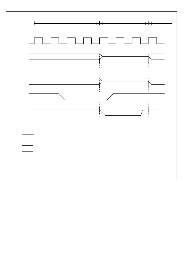
RD, WR
R/W, DS
D ≠D
7
0
A ≠A
19
0
¯
BREQ
BACK
Bus-right release cycle
CPU cycle
External access cycle
T
i
T
i
T
i
T
X
T
X
T
1
*
*
T
X
T
i
Fig. 3-15
(1)
(2)
(3)
(4)
(1) The BREQ pin is sampled at the start of a T
I
state and the Low level is detected.
(2) At the end of the internal operation cycle, the BACK pin goes Low and the CPU releases the bus.
(3) The BREQ pin is sampled at the T
X
state and a High level is detected.
(4) The BACK pin is returned to the High level, ending the bus-right release cycle.
*
T
I
: Internal CPU operation state.
T
X
: Bus-right released state.
Figure 3-15 Bus-Right Release Cycle (During Internal CPU Operation)
75

Notes: The BREQ signal must be held Low until BACK goes Low. If BREQ returns to the High
level before BACK goes Low, the bus release operation may be executed incorrectly.
To leave the bus-released state, the High level at the BREQ pin must be sampled two times. If the
BREQ returns to Low before it is sampled two times, the bus released cycle will not end.
The bus release operation is enabled only when the BRLE bit in the port 1 control register (P1CR)
is set to "1." When this bit is cleared to "0" (its initial value), the BREQ and BACK pins are used
for general-purpose input and output, as P1
3
and P1
2
.
An instruction that sets the BRLE bit is:
BSET.B #3, @H'FFFC
Note the following point when using the H8/532's release function.
If the BREQ signal is asserted and an interrupt is requested simultaneously during execution of the
SLEEP instruction, the BACK signal may fail to be output even though the CPU has released the
bus. This may cause the system to stop for the interval during which BREQ is asserted, with no
device in control of the bus. The interrupts that can cause this state include NMI, IRQ, and all the
interrupts from on-chip supporting modules. When the BREQ signal is deasserted, ending this
state, the CPU takes control of the bus again and resumes normal instruction execution.
The following methods can be used to avoid entering this state.
Method 1: If the BREQ signal is used, do not use the SLEEP instruction.
Method 2: Disable the BREQ signal during execution of the SLEEP instruction. This can be
done by clearing the bus release enable bit (BRLE) in the port 1 control register (P1CR) to 0
immediately bifore executing the SLEEP instruction. (When the BRLE bit is cleared, low inputs
on the BREQ line are not latched on-chip.) Place instructions to set the BRLE bit to 1 at the
beginning of interrupt-handling routines. If the data transfer controller (DTC) is used, place an
instruction to set the BRLE bit immediately after the SLEEP instruction.
If method 2 is used, BREQ inputs will be ignored while the chip is in sleep mode.
(Coding example)
Main Program
Interrupt-Handling Routine
BSET.B #3, @P1CR
BCLR.B #3, @P1CR
SLEEP
BSET.B #3, @P1CR
RTE
76

3.8.5 Reset State
In the reset state, the CPU and all on-chip supporting modules are initialized and placed in the
stopped state. The CPU enters the reset state whenever the RES pin goes Low, unless the CPU is
currently in the hardware standby mode. It remains in the reset state until the RES pin goes High.
See section 4.2, "Reset," for further information on the reset state.
3.8.6 Power-Down State
The power-down state comprises three modes: the sleep mode, the software standby mode, and
the hardware standby mode.
See section 18, "Power-Down State," for further information.
77

3.9 Programming Notes
3.9.1 Restriction on Address Location
The following restriction applies when instructions are located in on-chip RAM.
∑ Restriction
Instruction execution cannot proceed continuously from an external address to on-chip RAM in
the ZTAT versions. This restriction does not apply to versions with masked ROM.
∑ Solution
To execute instructions located in on-chip RAM, use a branch instruction (examples: Bcc, JMP,
etc.) to branch to the first instruction located in on-chip RAM. Do not place instruction code in
the last three bytes of external memory (H'FB7D to H'FB7F).
H'FB7A
H'FB7B
H'FB7C
H'FB7D
H'FB7E
H'FB7F
H'FB80
H'FB81
NOP
NOP
NOP
NOP
NOP
NOP
NOP
NOP
NOP
BRA
disp
NOP
NOP
Not
executable
Do not
place
instruction
code here
Branch
H'FB7A
H'FB7B
H'FB7C
H'FB7D
H'FB7E
H'FB7F
H'FB80
H'FB81
Execution Disabled
Execution Enabled
78

3.9.2 Note on MULXU Instruction
Note that in the case described below, the H8/532 multiply instruction does not give correct
results.
(1)
Problem
The result of a squaring operation such as MULXU.B Rn, Rn is indeterminate. This problem
occurs when the same register is specified for the source and destination of a byte
multiplication operation.
This problem occurs only in ZTAT versions of the H8/532. It does not occur in versions
with masked ROM.
(2)
Solution
The problem can be avoided by the following methods.
Place the source and destination operands in different registers.
Example: MULXU.B R4, R4
MOV.W R4, R5
MULXU.B R5, R4
Use a word multiplication instruction.
Example: MULXU.B R4, R4
MULXU.W R4, R4
MOV.W R5, R4
Place one of the operands in memory.
Example: MULXU.B R4, R4
MOV.W R4, @≠SP
MULXU.B @(1,SP), R4
ADDS #2, SP
This problem occurs only in the H8/532. It does not occur in other chips in the H8/500
Series (such as the H8/520).
(3)
Note on usage of C compiler
Programmers using the C compiler should bear the following programming note in mind.
∑ Conditions under which the compiler generates a MULXU.B Rn, Rn instruction
The C compiler generates a MULXU.B Rn, Rn instruction when the following two conditions
are satisfied in the source program:
79

A one-byte variable (char or unsigned char) is declared as a register variable.
The variable declared as in is squared by compound substitution
Example: register char a;
a *= a;
∑ Solution
The problem can be avoided as follows:
In the example above, do not declare the variable (a) as a register variable.
Example: register char a;
char a;
a *= a;
a *= a;
When squaring one-byte data, do not use compound substitution. Code as follows:
Example: a *= a;
a = a * a;
80

Section 4 Exception Handling
4.1 Overview
4.1.1 Types of Exception Handling and Their Priority
As indicated in table 4-1 (a) and (b), exception handling can be initiated by a reset, address error,
trace, interrupt, or instruction. An instruction initiates exception handling if the instruction is an
invalid instruction, a trap instruction, or a DIVXU instruction with zero divisor. Exception
handling begins with a hardware exception-handling sequence which prepares for the execution of
a user-coded software exception-handling routine.
There is a priority order among the different types of exceptions, as shown in table 4-1 (a). If two
or more exceptions occur simultaneously, they are handled in their order of priority. An
instruction exception cannot occur simultaneously with other types of exceptions.
Table 4-1 (a) Exceptions and Their Priority
Exception
Start of Exception-
Type
Source
Detection Timing
Handling Sequence
High
Reset
External
RES Low-to-High transition
Immediately
Address error
Internal
Instruction fetch or data read/write
End of instruction
bus cycle
execution
Trace
Internal
End of instruction execution, if
End of instruction
T = "1" in status register
execution
Interrupt
External,
End of instruction execution or end
End of instruction
Low
internal
of exception-handling sequence
execution
Table 4-1 (b) Instruction Exceptions
Exception Type
Start of Exception-Handling Sequence
Invalid instruction
Attempted execution of instruction with undefined code
Trap instruction
Started by execution of trap instruction
Zero divide
Attempted execution of DIVXU instruction with zero divisor
81

4.1.2 Hardware Exception-Handling Sequence
The hardware exception-handling sequence varies depending on the type of exception. When
exception handling is initiated by a factor other than a reset, the CPU:
1. Saves the program counter and status register (in minimum mode) or program counter, code
page register, and status register (in maximum mode) to the stack.
2. Clears the T bit in the status register to "0."
3. Fetches the start address of the exception-handling routine from the exception vector table.
4. Branches to that address.
For an interrupt, the CPU also alters the interrupt mask level in bits I2 to I0 of the status register.
For a reset, step 1 is omitted. See section 4.2, "Reset," for the full reset sequence.
4.1.3 Exception Factors and Vector Table
The factors that initiate exception handling can be classified as shown in figure 4-1.
The starting addresses of the exception-handling routines for each factor are contained in an
exception vector table located in the low addresses of page 0. The vector addresses are listed in
table 4-2. Note that there are different addresses for the minimum and maximum modes.
82
Exception
∑ Reset
∑ Interrupt
∑ Address error
∑ Instruction
∑ Trace
External
interrupt
Internal
interrupt
Invalid instruction
Zero divide
TRAPA instruction
TRAP/VS instruction
NMI
IRQ
0
IRQ
1
Internal interrupt requested by
on-chip module
Figure 4-1 Types of Factors Causing Exception Handling
83

Table 4-2 Exception Vector Table
Vector Address
Type of Exception
Minimum Mode
Maximum Mode
*
1
Reset (initialize PC)
H'0000 to H'0001
H'0000 to H'0003
-- (Reserved for system)
H'0002 to H'0003
H'0004 to H'0007
Invalid instruction
H'0004 to H'0005
H'0008 to H'000B
DIVXU instruction (zero divide)
H'0006 to H'0007
H'000C to H'000F
TRAP/VS instruction
H'0008 to H'0009
H'0010 to H'0013
H'000A to H'000B
H'0014 to H'0017
-- (Reserved for system)
to
to
H'000E to H'000F
H'001C to H'001F
Address error
H'0010 to H'0011
H'0020 to H'0023
Trace
H'0012 to H'0013
H'0024 to H'0027
-- (Reserved for system)
H'0014 to H'0015
H'0028 to H'002B
Nonmaskable external interrupt (NMI)
H'0016 to H'0017
H'002C to H'002F
H'0018 to H'0019
H'0030 to H'0033
-- (Reserved for system)
to
to
H'001E to H'001F
H'003C to H'003F
TRAPA instruction (16 vectors)
H'0020 to H'0021
H'0040 to H'0043
to
to
H'003E to H'003F
H'007C to H'007F
External interrupts
IRQ
0
H'0040 to H'0041
H'0080 to H'0083
IRQ
1
H'0042 to H'0043
H'0084 to H'0087
Internal interrupts
*
2
H'0044 to H'0045
H'0088 to H'008B
to
to
H'007E to H'007F
H'00FC to H'00FF
Notes:
*
1. The exception vector table is located at the beginning of page 0.
*
2. For details of the internal interrupt vectors, see table 5-2.
84

4.2 Reset
4.2.1 Overview
A reset has the highest exception-handling priority.
When the RES pin goes Low, all current processing is halted and the H8/532 chip enters the reset
state.
A reset initializes the internal status of the CPU and the registers of the on-chip supporting
modules and I/O ports. It does not initialize the on-chip RAM.
When the RES pin returns from Low to High, the H8/532 chip comes out of the reset state and
begins executing the hardware reset sequence.
4.2.2 Reset Sequence
The Reset signal is detected when the RES pin goes Low.
To ensure that the H8/532 is reset, the RES pin should be held Low for at least 20ms at power-up.
To reset the H8/532 during operation, the RES pin should be held Low for at least 6 ¯ clock
cycles. See table D-1, "Status of Ports" in Appendix D for the status of other pins in the reset
state.
When the RES pin returns to the High state after being held Low for the necessary time, the
hardware reset exception-handling sequence begins, during which:
1. The value at the mode pins (MD
2
to MD
0
) is latched in bits MDS2 to MDS0 of the mode
control register (MDCR).
2. In the status register (SR), the T bit is cleared to disable the trace mode, and the interrupt mask
level (bits I2 to I0) is set to 7. A reset disables all interrupts, including NMI.
3. The CPU loads the reset start address from the vector table into the program counter and begins
executing the program at that address.
The contents of the vector table differs between minimum mode and maximum mode as indicated
in figure 4-2. This affects step 3 as follows:
Minimum mode: One word is copied from addresses H'0000 and H'0001 in the vector table to
the program counter. Program execution then begins from the address in the program counter
(PC).
85

Maximum Mode: Two words are read from addresses H'0000 to H'0003 in the vector table. The
byte in address H'0000 is ignored. The byte in address H'0001 is copied to the code page register
(CP). The contents of addresses H'0002 and H'0003 are copied to the program counter. Program
execution starts from the address indicated by the code page register and program counter.
Figure 4-3 shows the timing of the reset sequence in minimum mode. Figure 4-4 shows the
timing of the reset sequence in maximum mode.
4.2.3 Stack Pointer Initialization
The hardware reset sequence does not initialize the stack pointer, so this must be done by
software. If an interrupt were to be accepted after a reset and before the stack pointer (SP) is
initialized, the program counter and status register would not be saved correctly, causing a
program crash. This danger can be avoided by coding the reset routine as explained next.
When the chip comes out of the reset state all interrupts, including NMI, are disabled, so the
instruction at the reset start address is always executed. In the minimum mode, this instruction
should initialize the stack pointer (SP). In the maximum mode, this instruction should be an LDC
instruction initializing the stack page register (TP), and the next instruction should initialize the
stack pointer. Execution of the LDC instruction disables interrupts again, ensuring that the stack
pointer initializing instruction is executed.
H'0000
PC (Upper)
H'0001
PC (Lower)
(1) Minimum mode
H'0000
Don't care
H'0001
CP
(2) Maximum mode
H'0002
PC (Upper)
H'0003
PC (Lower)
Figure 4-2 Reset Vector
86
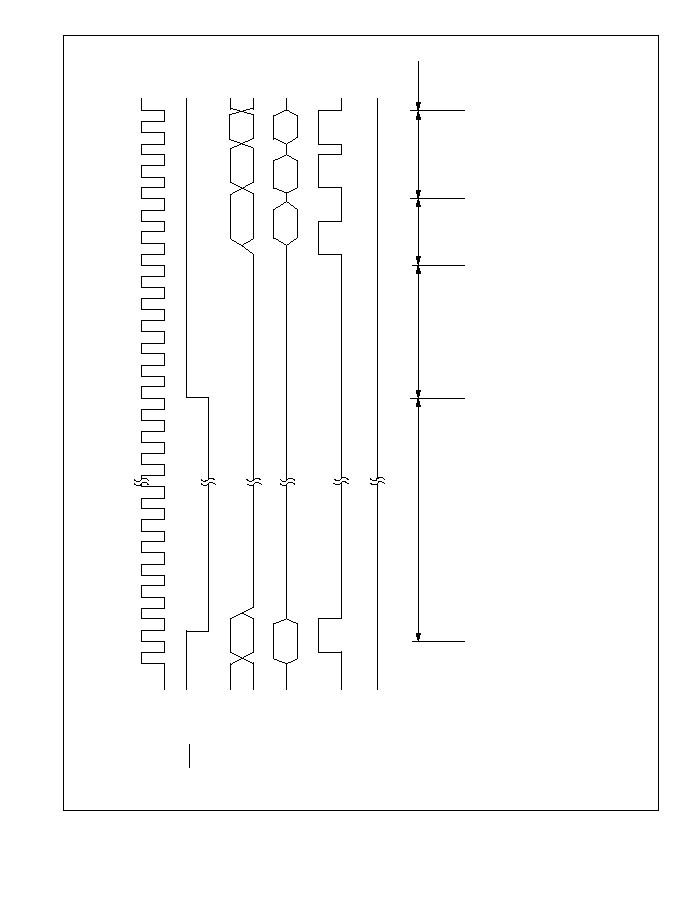
¯
RES
Internal
address
bus
Internal data
bus (16 bits)
Internal
Read
signal
Internal
Write
signal
(1)
(2)
Vector
address
Vector
(4)
(3)
Instruction
execution
cycle
Prefetch first
instruction
of program
Reset
vector
Internal processing cycle
Minimum 6 states
(1) Instruction prefetch address
(2) Operation code
(3) Program start address
(4) First instruction of program
Note:
This timing chart applies to the minimum mode when the program and stack areas are both in on-chip memory and the program start
s at an even address.
Fig. 4-3
Figure 4-3 Reset Sequence (Minimum Mode, On-Chip Memory)
87
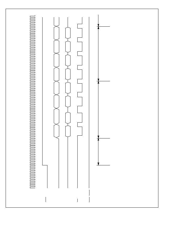
(1)
Vector address
Vector
address + 1
Vector
address + 2
Vector
address + 3
(2)
Internal processing
cycle
Note:
This diagram applies to maximum mode when the program area and vector table are both in external memory.
After a reset, the wait-state controller inserts three wait states in each bus cycle.
(1) Program start address
(2) First instruction of program
Reset vector
Prefetch first instruction of program
Instruction
execution
cycle
¯
RES
RD
LWR, HWR
D to D
15
0
A to A
23
0
don't care
Vector
CP
Vector
PC
Vector
PC
HL
Read signal
Write signal
Figure 4-4 Reset Sequence (Maximum Mode, External Memory)
88

4.3 Address Error
There are three causes of address errors:
∑ Illegal instruction prefetch
∑ Word data access at odd address
∑ Off-chip access in single-chip mode
An address error initiates the address error exception-handling sequence. This sequence clears the
T bit of the status register to "0" to disable the trace mode, but does not affect the interrupt mask
level in bits I2 to I0.
4.3.1 Illegal Instruction Prefetch
An attempt to prefetch an instruction from the register field in memory addresses H'FF80 to
H'FFFF causes an address error regardless of the MCU operating mode.
Handling of this address error begins when the prefetch cycle that caused the error has been
completed and execution of the current instruction has also been completed. The program counter
value pushed on the stack is the address of the instruction immediately following the last
instruction executed.
Program code should not be located in addresses H'FF7D to H'FF7F. If the CPU executes an
instruction in these addresses, it will attempt to prefetch the next instruction from the register
field, causing an address error.
4.3.2 Word Data Access at Odd Address
If an attempt is made to access word data starting at an odd address, an address error occurs
regardless of the MCU operating mode. The program counter value pushed on the stack in the
handling of this error is the address of the next instruction (or next but one) after the instruction
that attempted the illegal word access.
4.3.3 Off-Chip Address Access in Single-Chip Mode
In the single-chip mode there is no external memory, so in addition to the address errors described
above, the following two types of address errors can occur.
Access to Addresses H'8000 to H'FB7F: These addresses exist neither in on-chip ROM or RAM
nor in the on-chip register field, so an address error occurs if they are accessed for any purpose:
for instruction prefetch, byte data access, or word data access.
89

Access to Disabled RAM Area: The on-chip RAM area (H'FB80 to H'FF7F) can be disabled by
clearing the RAME bit in the RAM control register (RAMCR). If RAM access is attempted in
this state in the single-chip mode, an address error occurs.
4.4 Trace
When the T bit of the status register is set to "1," the CPU operates in trace mode. A trace
exception occurs at the completion of each instruction. The trace mode can be used to execute a
program for debugging by a debugger.
In the trace exception sequence the T bit of the status register is cleared to "0" to disable the trace
mode while the trace routine is executing. The interrupt mask level in bits I2 to I0 is not changed.
Interrupts are accepted as usual during the trace routine.
In the status-register data saved on the stack, the T bit is set to "1." When the trace routine returns
with the RTE instruction, the status register is popped from the stack and the trace mode resumes.
If an address error occurs during execution of the first instruction after the return from the trace
routine, since the address error has higher priority, the address error exception-handling sequence
is initiated, clearing the T bit in the status register to "0" and making it impossible to trace this
instruction.
4.5 Interrupts
Interrupts can be requested from three external sources (NMI, IRQ
0
, and IRQ
1
) and seven on-chip
supporting modules: the 16-bit free-running timers (FRT1 to FRT3), the 8-bit timer, the serial
communication interface (SCI), the A/D converter, and the watchdog timer (WDT). The on-chip
interrupt sources can request a total of nineteen different types of interrupts, each having its own
interrupt vector. Figure 4-5 lists the interrupt sources and the number of different interrupts from
each source.
Each interrupt source has a priority. NMI interrupts have the highest priority, and are normally
accepted unconditionally. The priorities of the other interrupt sources are set in control registers
(IPR A to D) in the register field at the high end of page 0 and can be changed by software.
Priority levels range from 0 (low) to 7 (high), with NMI considered to be on level 8.
The on-chip interrupt controller decides whether an interrupt can be accepted by comparing its
priority with the interrupt mask level, and determines the order in which to accept competing
interrupt requests. Interrupts that are not accepted immediately remain pending until they can be
accepted later.
90

When it accepts an interrupt, the interrupt controller also decides whether to interrupt the CPU or
start the on-chip data transfer controller (DTC). This decision is controlled by bits set in four data
transfer enable registers (DTE A to D) in the register field. The DTC is started if the corresponding
DTE bit is set to "1;" otherwise a CPU interrupt is generated. DTC interrupts provide an efficient
way to send and receive blocks of data via the serial communication interface, or to transfer data
between memory and I/O without detailed CPU programming. The CPU stops while the DTC is
operating. DTC interrupts are described in section 6, "Data Transfer Controller."
The hardware exception-handling sequence for a CPU interrupt clears the T bit in the status
register to "0" and sets the interrupt mask level in bits I2 to I0 to the level of the interrupt it has
accepted. This prevents the interrupt-handling routine from being interrupted except by a higher-
level interrupt. The previous interrupt mask level is restored on the return from the interrupt-
handling routine.
For further information on interrupts, see section 5, "Interrupt Controller."
Interrupt
sources
Internal
interrupts
NMI (1)
IRQ
0
(1)
IRQ
1
(1)
16-Bit FRT1 (4)
16-Bit FRT2 (4)
16-Bit FRT3 (4)
8-Bit timer (3)
SCI (3)
A/D converter (1)
WDT
*
NMI:
NonMaskable Interrupt
IRQ:
Interrupt Request
FRT:
Free-Running Timer
SCI:
Serial Communication Interface
WDT:
WatchDog Timer
*
Interrupts from the watchdog timer are handled as NMI or IRQ
0
.
External
interrupts
Figure 4-5 Interrupt Sources (and Number of Interrupt Types)
91

4.6 Invalid Instruction
An invalid instruction exception occurs if an attempt is made to execute an instruction with an
undefined operation code or illegal addressing mode specification. The program counter value
pushed on the stack is the value of the program counter when the invalid instruction code was
detected.
In the invalid instruction exception-handling sequence the T bit of the status register is cleared to
"0," but the interrupt mask level (I2 to I0) is not affected.
4.7 Trap Instructions and Zero Divide
A trap exception occurs when the TRAPA or TRAP/VS instruction is executed. A zero divide
exception occurs if an attempt is made to execute a DIVXU instruction with a zero divisor.
In the exception-handling sequences for these exceptions the T bit of the status register is cleared
to "0," but the interrupt mask level (I2 to I0) is not affected. If a normal interrupt is requested
while a trap or zero-divide instruction is being executed, after the trap or zero-divide exception-
handling sequence, the normal interrupt exception-handling sequence is carried out.
TRAPA Instruction: The TRAPA instruction always causes a trap exception. The TRAPA
instruction includes a vector number from 0 to 15, allowing the user to provide up to sixteen
different trap-handling routines.
TRAP/VS Instruction: When the TRAP/VS instruction is executed, a trap exception occurs if
the overflow (V) bit in the condition code register is set to "1." If the V bit is cleared to "0," no
exception occurs and the next instruction is executed.
DIVXU Instruction with Zero Divisor: An exception occurs if an attempt is made to divide
by zero in a DIVXU instruction.
4.8 Cases in Which Exception Handling is Deferred
In the cases described next, the address error exception, trace exception, external interrupt (NMI,
IRQ
0
, and IRQ
1
) requests, and internal interrupt requests (19 types) are not accepted immediately
but are deferred until after the next instruction has been executed.
4.8.1 Instructions that Disable Interrupts
Interrupts are disabled immediately after the execution of five instructions: XORC, ORC, ANDC,
LDC, and RTE.
Suppose that an internal interrupt is requested and the interrupt controller, after checking the
interrupt priority and interrupt mask level, notifies the CPU of the interrupt, but the CPU is
92

currently executing one of the five instructions listed above. After executing this instruction the
CPU always proceeds to the next instruction. (And if the next instruction is one of these five, the
CPU also proceeds to the next instruction after that.) The exception-handling sequence starts after
the next instruction that is not one of these five has been executed. The following is an example:
(Example)
4.8.2 Disabling of Exceptions Immediately after a Reset
If an interrupt is accepted after a reset and before the stack pointer (SP) is initialized, the program
counter and status register will not be saved correctly, leading to a program crash. To prevent this,
when the chip comes out of the reset state all interrupts, including the NMI, are disabled, so the
first instruction of the reset routine is always executed. As noted earlier, in the minimum mode,
this instruction should initialize the stack pointer (SP). In the maximum mode, the first instruction
should be an LDC instruction that initializes the stack page register (TP); the next instruction
should initialize the stack pointer.
4.8.3 Disabling of Interrupts after a Data Transfer Cycle
If an interrupt starts the data transfer controller and another interrupt is requested during the data
transfer cycle, when the data transfer cycle ends, the CPU always executes the next instruction
before handling the second interrupt.
Even if a nonmaskable interrupt (NMI) occurs during a data transfer cycle, it is not accepted until
the next instruction has been executed. An example of this is shown below.
LDC.B #H'00,TP
MOV.B #H'00,@WCR
Program flow
Interrupt controller notifies CPU
of interrupt request
To exception-handling sequence
MOV.W #H'FF80,SP
CPU executes the instruction next to LDC before
starting exception handling
.
.
.
.
.
.
.
.
.
93
4.9 Stack Status after Completion of Exception Handling
The status of the stack after an exception-handling sequence is described below.
Table 4-3 shows the stack after completion of the exception-handling sequence for various types
of exceptions in the minimum and maximum modes.
Table 4-3 Stack after Exception Handling Sequence
Note: The RTE instruction returns to the next instruction after the instruction being executed when
the exception occurred.
DTC interrupt request
MOV.W R0,@H'FF00
Program flow
To NMI exception-handling sequence
NMI interrupt request
After data transfer cycle, CPU
executes next instruction before
branching to exception handling
ADD.W R2,R0
MOV.W #H'FF02,R0
Data transfer cycle
(Example)
.
.
.
.
.
.
.
.
Exception Factor
Minimum Mode
Maximum Mode
Trace
Interrupt
Trap
Zero divide
(DIVXU)
SP
SR (upper byte)
TP:SP
SR (upper byte)
SR (lower byte)
SR (lower byte)
Next instruction address (upper byte)
Don't-care
Next instruction address (lower byte)
Next instruction page (8 bits)
Next instruction address (upper byte)
Next instruction address (lower byte)
94

Table 4-3 Stack after Exception Handling Sequence (cont)
Note: The program counter value pushed on the stack is not necessarily the address of the first
byte of the invalid instruction.
Note: The program counter value pushed on the stack is the address of the next instruction after
the last instruction successfully executed.
Exception Factor
Minimum Mode
Maximum Mode
Invalid
instruction
SP
SR (upper byte)
TP:SP
SR (upper byte)
SR (lower byte)
SR (lower byte)
PC when error occurred (upper byte)
Don't-care
PC when error occurred (lower byte)
CP when error occurred (8 bits)
PC when error occurred (upper byte)
PC when error occurred (lower byte)
Address
error
SP
SR (upper byte)
TP:SP
SR (upper byte)
SR (lower byte)
SR (lower byte)
PC when error occurred (upper byte)
Don't-care
PC when error occurred (lower byte)
CP when error occurred (8 bits)
PC when error occurred (upper byte)
PC when error occurred (lower byte)
95

4.9.1 PC Value Pushed on Stack for Trace, Interrupts, Trap Instructions, and Zero Divide
Exceptions
The program counter value pushed on the stack for a trace, interrupt, trap, or zero divide exception
is the address of the next instruction at the time when the interrupt was accepted. The RTE
instruction accordingly returns to the next instruction after the instruction executed before the
exception-handling sequence.
4.9.2 PC Value Pushed on Stack for Address Error and Invalid Instruction Exceptions
The program counter value pushed on the stack for an address error or invalid instruction
exception differs depending on the conditions when the exception occurred.
4.10 Notes on Use of the Stack
If the stack pointer is set to an odd address, an address error will occur when the stack is accessed
during interrupt handling or for a subroutine call. The stack pointer should always point to an
even address. To keep the stack pointer pointing to an even address, a program should use word
data size when saving or restoring registers to and from the stack.
In the @≠SP or @SP+ addressing mode, the CPU performs word access even if the instruction
specifies byte size. (This is not true in the @≠Rn and @Rn+ addressing modes when Rn is a
register from R0 to R6.)
96

Section 5 Interrupt Controller
5.1 Overview
The interrupt controller decides which interrupts to accept, and how to deal with multiple
interrupts. It also decides whether an interrupt should be served by the CPU or by the data
transfer controller (DTC). This section explains the features of the interrupt controller, describes
its internal structure and control registers, and details the handling of interrupts.
For detailed information on the data transfer controller, see section 6, "Data Transfer Controller."
5.1.1 Features
Three main features of the interrupt controller are:
∑ Interrupt priorities are user-programmable.
User programs can set priority levels from 7 (high) to 0 (low) in four interrupt priority (IPR)
registers for IRQ
0
, IRQ
1
, and each of the on-chip supporting modules--for every interrupt, that
is, except the nonmaskable interrupt (NMI). NMI has the highest priority level (8) and is
normally always accepted. An interrupt with priority level 0 is always masked.
∑ Multiple interrupts on the same level are served in a default priority order.
Lower-priority interrupts remain pending until higher-priority interrupts have been handled.
∑ For most interrupts, software can select whether to have the interrupt served by the CPU or the
on-chip data transfer controller (DTC).
User programs can make this selection by setting and clearing bits in four data transfer enable
(DTE) registers. The data transfer controller can be started by any interrupts except NMI, the
error interrupt (ERI) from the on-chip serial communication interface, and the overflow
interrupts (FOVI and OVI) from the on-chip timers.
97
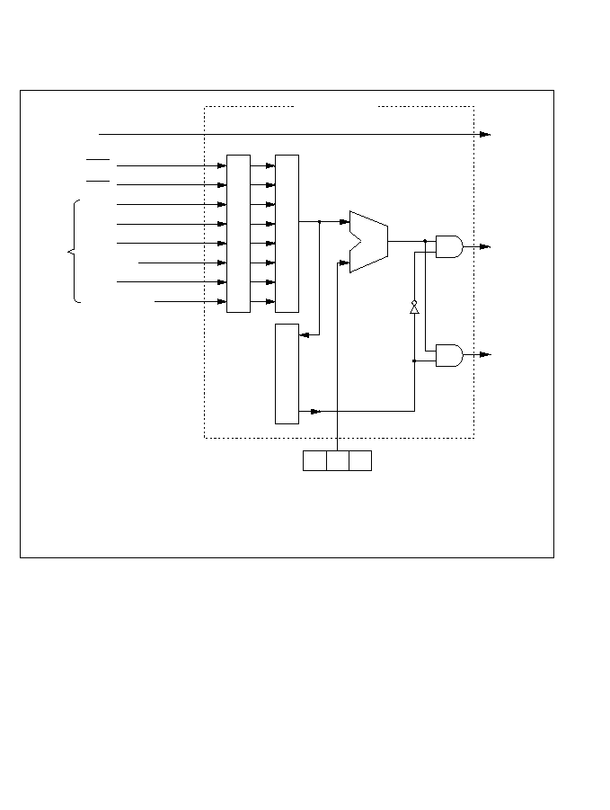
5.1.2 Block Diagram
Figure 5-1 shows the block configuration of the interrupt controller.
IRQ0
IRQ1
FRT1
FRT2
FRT3
8 bits timer
SCI
A/D converter
NMI
Interrupt
request
signals
from
modules
Interrupt controller
NMI
request
Interrupt
request
DTC
request
Com-
parator
Priority decision
IPRA to IPRD
DTEA to DTED
I 2
I 1
I 0
SR (CPU)
FRT:
SCI:
SR:
IPR:
DTE:
16 Bits Free Running Timer
Serial Communication Interface
Status Register
Interrupt Priority Register
Data Transfer Enable Register
Figure 5-1 Interrupt Controller Block Diagram
98

5.1.3 Register Configuration
The four interrupt priority registers (IPRA to IPRD) and four data transfer enable registers (DTEA
to DTED) are 8-bit registers located at addresses H'FFF0 to H'FFF7 in the register field in page 0
of the address space. Table 5-1 lists their attributes.
Table 5-1 Interrupt Controller Registers
5.2 Interrupt Types
There are 22 distinct types of interrupts: 3 external interrupts originating off-chip and 19 internal
interrupts originating in the on-chip supporting modules.
5.2.1 External Interrupts
The three external interrupts are NMI, IRQ
0
, and IRQ
1
.
NMI (NonMaskable Interrupt): This interrupt has the highest priority level (8) and cannot be
masked. An NMI is generated by input to the NMI pin, and can also be generated by a watchdog
timer (WDT) overflow. The input at the NMI pin is edge-sensed. A user program can select
whether to have the interrupt occur on the rising edge or falling edge of the NMI input by setting
or clearing the nonmaskable interrupt edge bit (NMIEG) in the port 1 control register (P1CR).
In the NMI exception-handling sequence, the T (Trace) bit in the CPU status register (SR) is
cleared to "0," and the interrupt mask level in I2 to I0 is set to 7, masking all other interrupts. The
interrupt controller holds the NMI request until the NMI exception-handling sequence begins, then
clears the NMI request, so if another interrupt is requested at the NMI pin during the NMI
exception-handling sequence, the NMI exception-handling sequence will be carried out again.
A watchdog timer overflow generates an NMI if the TME and WT/IT bits in the watchdog timer's
status/control register are both set to "1." See section 13, "Watchdog Timer" for details.
Name
Abbreviation
Read/Write
Address
Initial Value
Interrupt
A
IPRA
R/W
H'FFF0
H'00
priority
B
IPRB
R/W
H'FFF1
H'00
register
C
IPRC
R/W
H'FFF2
H'00
D
IPRD
R/W
H'FFF3
H'00
Data transfer
A
DTEA
R/W
H'FFF4
H'00
enable
B
DTEB
R/W
H'FFF5
H'00
register
C
DTEC
R/W
H'FFF6
H'00
D
DTED
R/W
H'FFF7
H'00
99

Coding Examples:
To select the rising edge of the NMI input:
BSET.B #4, @H'FFFC
To select the falling edge of the NMI input:
BCLR.B #4, @H'FFFC
IRQ
0
(Interrupt Request 0): An IRQ
0
interrupt can be requested by a Low input to the IRQ
0
pin
and/or a watchdog timer overflow. A Low IRQ
0
input requests an IRQ
0
interrupt if the interrupt
request enable 0 bit (IRQ
0
E) in the P1CR is set to "1." IRQ
0
must be held Low until the CPU
accepts the interrupt. Otherwise the request will be ignored. A watchdog timer overflow requests
an IRQ
0
interrupt if the TME bit is set to "1" and the WT/IT bit is cleared to "0" in the watchdog
timer's control/status register. See section 13, "Watchdog Timer" for details of the watchdog
timer.
The IRQ
0
interrupt can be assigned any priority level from 7 to 0 by setting the corresponding
value in the upper four bits of IPRA. If bit 4 of data transfer enable register A (DTEA) is set to
"1," an IRQ
0
interrupt starts the data transfer controller. Otherwise the interrupt is served by the
CPU.
In the CPU interrupt-handling sequence for IRQ
0
, the T bit of the status register is cleared to "0,"
and the interrupt mask level is set to the value in the upper four bits of IPRA.
Coding Examples:
To enable IRQ
0
to be requested by IRQ
0
input:
BSET.B #5, @H'FFFC
To assign priority level 7 to IRQ
0
:
OR.B #70, @H'FFF0
To have IRQ
0
start the DTC:
BSET.B #4, @H'FFF4
IRQ
1
(Interrupt Request 1): An IRQ
0
interrupt is requested by a High-to-Low transition at the
IRQ
1
pin. The IRQ
1
interrupt is enabled only when the interrupt request enable 1 bit (IRQ
1
E) in
the P1CR is set to "1."
The IRQ
1
interrupt can be assigned any priority level from 7 (high) to 0 (low) by setting the
corresponding value in the lower four bits of IPRA. If bit 0 of data transfer enable register A
(DTEA) is set to "1," an IRQ
1
interrupt starts the data transfer controller. Otherwise the interrupt
is served by the CPU.
The interrupt controller holds the IRQ
1
request until the IRQ
1
exception-handling sequence
begins, then clears the IRQ
1
request. If another interrupt is requested at the IRQ
1
pin during the
IRQ
1
interrupt-handling routine, the request is held, but the IRQ
1
exception-handling sequence is
not carried out immediately because the interrupt is masked by bits I2 to I0 in the status register.
On return from the interrupt-handling routine one more instruction is executed, then the
exception-handling sequence for the second IRQ
1
interrupt is carried out.
100

In the CPU interrupt-handling sequence for IRQ
1
, the T bit of the CPU status register is cleared to
"0," and the interrupt mask level is set to the value in the lower four bits of IPRA.
Coding Examples:
To enable IRQ
1
to be requested by IRQ
1
input:
BSET.B #6, @H'FFFC
To assign priority level 7 to IRQ
0
and level 5 to IRQ
1
:
MOV.B #75, @H'FFF0
To have IRQ
1
start the DTC:
BSET.B #0, @H'FFF4
5.2.2 Internal Interrupts
Nineteen types of internal interrupts can be requested by the on-chip supporting modules. Each
interrupt is separately vectored in the exception vector table, so it is not necessary for the user-
coded interrupt handler routine to determine which type of interrupt has occurred.
Each of the internal interrupts can be enabled or disabled by setting or clearing an enable bit in the
control register of the on-chip supporting module.
An interrupt priority level from 7 to 0 can be assigned to each on-chip supporting module by
setting interrupt priority registers B to D. Within each module, different interrupts have a fixed
priority order. For most of these interrupts, values set in data transfer enable registers B to D can
select whether to have the interrupt served by the CPU or the data transfer controller.
In the CPU interrupt-handling sequence, the T bit of the CPU status register is cleared to "0," and
the interrupt mask level in bits I2 to I0 is set to the value in the IPR.
5.2.3 Interrupt Vector Table
Table 5-2 lists the addresses of the exception vector table entries for each interrupt, and explains
how their priority is determined. For the on-chip supporting modules, the priority level set in the
interrupt priority register applies to the module as a whole: all interrupts from that module have
the same priority level. A separate priority order is established among interrupts from the same
module. If the same priority level is assigned to two or more modules and two interrupts are
requested simultaneously from these modules, they are served in the priority order indicated in the
rightmost column in table 5-2.
A reset clears the interrupt priority registers so that all interrupts except NMI start with priority
level 0, meaning that they are unconditionally masked.
101

Table 5-2 Interrupts, Vectors, and Priorities
*
If two or more interrupts are requested simultaneously, they are handled in order of priority level,
as set in registers IPRA to IPRD. If they have the same priority level because they are requested
from the same on-chip supporting module, they are handled in a fixed priority order within the
module. If they are requested from different modules to which the same priority level is
assigned, they are handled in the order indicated in the right-hand column.
Assignable
Priority
Priority
Vector Table
among
Levels
Priority
Entry Address
Interrupts
(Initial IPR
within
Minimum
Maximum
on
Same
Interrupt
Level)
Bits
Module
Mode
Mode
Level
*
NMI
8
--
--
H'16 - H'17
H'2C - H'2F
High
(8)
IRQ
0
7 to 0
IPRA
--
H'40 - H'41
H'80 - H'83
(0)
bits 6 to 4
IRQ
1
7 to 0
IPRA
--
H'42 - H'43
H'84 - H'87
(0)
bits 2 to 0
16-Bit
ICI
7 to 0
IPRB
3
H'48 - H'49
H'90 - H'93
FRT1
OCIA
(0)
bits 6 to 4
2
H'4A - H'4B
H'94 - H'97
OCIB
1
H'4C - H'4D
H'98 - H'9B
FOVI
0
H'4E - H'4F
H'9C - H'9F
16-Bit
ICI
7 to 0
IPRB
3
H'50 - H'51
H'A0 - H'A3
FRT2
OCIA
(0)
bits 2 to 0
2
H'52 - H'53
H'A4 - H'A7
OCIB
1
H'54 - H'55
H'A8 - H'AB
FOVI
0
H'56 - H'57
H'AC - H'AF
16-Bit
ICI
7 to 0
IPRC
3
H'58 - H'59
H'B0 - H'B3
FRT3
OCIA
(0)
bits 6 to 4
2
H'5A - H'5B
H'B4 - H'B7
OCIB
1
H'5C - H'5D
H'B8 - H'BB
FOVI
0
H'5E - H'5F
H'BC - H'BF
8-Bit
CMIA
7 to 0
IPRC
2
H'60 - H'61
H'C0 - H'C3
timer
CMIB
(0)
bits 2 to 0
1
H'62 - H'63
H'C4 - H'C7
OVI
0
H'64 - H'65
H'C8 - H'CB
SCI
ERI
7 to 0
IPRD
2
H'68 - H'69
H'D0 - H'D3
RXI
(0)
bits 6 to 4
1
H'6A - H'6B
H'D4 - H'D7
TXI
0
H'6C - H'6D
H'D8 - H'DB
A/D
ADI
7 to 0
IPRD
--
H'70 - H'71
H'E0 - H'E3
converter
(0)
bits 2 to 0
Low
102
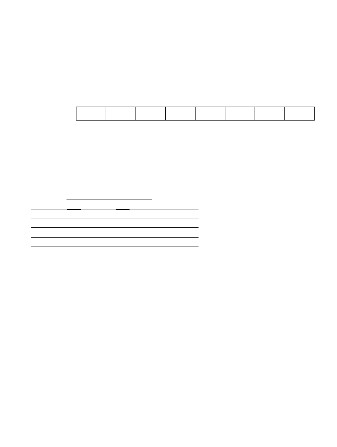
5.3 Register Descriptions
5.3.1 Interrupt Priority Registers A to D (IPRA to IPRD)
IRQ
0
, IRQ
1
, and the on-chip supporting modules are each assigned three bits in one of the four
interrupt priority registers (IPRA to IPRD). These bits specify a priority level from 7 (high) to 0
(low) for interrupts from the corresponding source. The drawing below shows the configuration
of the interrupt priority registers. Table 5-3 lists their assignments to interrupt sources.
Note: Bits 7 and 3 are reserved. They cannot be modified and are always read as "0."
Table 5-3 Assignment of Interrupt Priority Registers
As table 5-3 indicates, each interrupt priority register specifies priority levels for two interrupt
sources. A user program can assign desired levels to these interrupt sources by writing "000" in
bits 6 to 4 or bits 2 to 0 to set priority level 0, for example, or "111" to set priority level 7.
A reset clears registers IPRA to IPRD to H'00, so all interrupts except NMI are initially masked.
Bit
7
6
5
4
3
2
1
0
--
--
Initial value
0
0
0
0
0
0
0
0
Read/Write
R
R/W
R/W
R/W
R
R/W
R/W
R/W
Interrupt Request Source
Register
Bits 6 to 4
Bits 2 to 0
Address
IPRA
IRQ
0
IRQ
1
H'FFF0
IPRB
16-Bit FRT1
16-Bit FRT2
H'FFF1
IPRC
16-Bit FRT3
8-Bit timer
H'FFF2
IPRD
SCI
A/D converter
H'FFF3
103

When the interrupt controller receives one or more interrupt requests, it selects the request with
the highest priority and compares its priority level with the interrupt mask level set in bits I2 to I0
in the CPU status register. If the priority level is higher than the mask level, the interrupt
controller passes the interrupt request to the CPU (or starts the data transfer controller). If the
priority level is lower than the mask level, the interrupt controller leaves the interrupt request
pending until the interrupt mask is altered to a lower level or the interrupt priority is raised.
Similarly, if it receives two interrupt requests with the same priority level, the interrupt controller
determines their priority as explained in table 5-2 and leaves the interrupt request with the lower
priority pending.
5.3.2 Timing of Priority Setting
The interrupt controller requires two system clock (¯) periods to determine the priority level of an
interrupt. Accordingly, when an instruction modifies an instruction priority register, the new
priority does not take effect until after the next instruction has been executed.
5.4 Interrupt Handling Sequence
5.4.1 Interrupt Handling Flow
The interrupt-handling sequence follows the flowchart in figure 5-2. Note that address error, trace
exception, and NMI requests bypass the interrupt controller's priority decision logic and are
routed directly to the CPU.
1. Interrupt requests are generated by one or more on-chip supporting modules or external
interrupt sources.
2. The interrupt controller checks the interrupt priorities set in IPRA to IPRD and selects the
interrupt with the highest priority. Interrupts with lower priorities remain pending. Among
interrupts with the same priority level, the interrupt controller determines priority as explained
in table 5-2.
3. The interrupt controller compares the priority level of the selected interrupt request with the
mask level in the CPU status register (bits I2 to I0). If the priority level is equal to or less than
the mask level, the interrupt request remains pending. If the priority level is higher than the
mask level, the interrupt controller accepts the interrupt request and proceeds to the next step.
4. The interrupt controller checks the corresponding bit (if any) in the data transfer enable
registers (DTEA to DTED). If this bit is set to "1," the data transfer controller is started.
Otherwise, the CPU interrupt exception-handling sequence is started.
When the data transfer controller is started, the interrupt request is cleared (except for interrupt
requests from the serial communication interface, which are cleared by writing to the TDR or
reading the RDR).
104

If the data transfer enable bit is cleared to "0" (or is nonexistent), the sequence proceeds as
follows. For the case in which the data transfer controller is started, see section 6, "Data Transfer
Controller."
5. After the CPU has finished executing the current instruction, the program counter and status
register (in minimum mode) or program counter, code page register, and status register (in
maximum mode) are saved to the stack, leaving the stack in the condition shown in figure 5-3
(a) or (b). The program counter value saved on the stack is the address of the next instruction
to be executed.
6. The T (Trace) bit of the status register is cleared to "0," and the priority level of the interrupt is
copied to bits I2 to I0, thus masking further interrupts unless they have a higher priority level.
When an NMI is accepted, the interrupt mask level in bits I2 to I0 is set to 7.
7. The interrupt controller generates the vector address of the interrupt, and the entry at this
address in the exception vector table is read to obtain the starting address of the user-coded
interrupt handling routine.
In step 7, the same difference between the minimum and maximum modes exists as in the reset
handling sequence. In the minimum mode, one word is copied from the vector table to the
program counter, then the interrupt-handling routine starts executing from the address indicated in
the program counter. In the maximum mode, two words are read. The lower byte of the first word
is copied to the code page register. The second word is copied to the program counter. The
interrupt-handling routine starts executing from the address indicated in the code page register and
program counter.
105
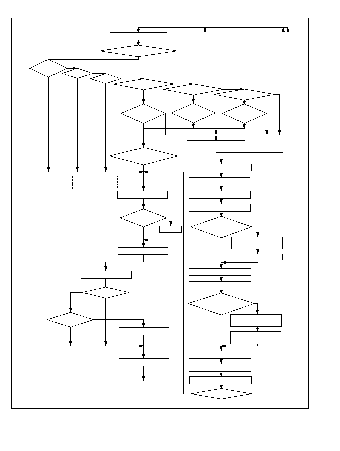
Program execution state
Interrupt requested?
Y
N
N
N
N
N
N
N
N
N
N
Y
Y
Y
Y
Y
Y
Y
Y
Y
Y
N
N
Y
Y
N
N
N
N
Y
Y
Y
N
Address
error?
Trace?
NMI?
Level-7 interrupt?
Level-6 interrupt?
Level-1 interrupt?
Mask level
in SR 6?
Mask level
in SR 5?
Mask level
in SR = 0?
Data transfer
enabled?
Interrupt remains pending
Start DTC
Read DTC vector
Read transfer mode
Read source address
Read data
Source
address increment
mode?
Increment source
address (+1 or +2)
Write source address
Read destination address
Write data
Exception-handling
sequence
Save PC
Maximum
mode?
Save SR
Save PC
Clear T bit
Trace
Address
error?
Update mask level
Vectoring
Destination
address increment
mode?
Write destination
address
Increment source
address (+1 or +2)
Read DTCR
DTCR-1 DTCR
Write DTCR
DTCR = 0?
To user-coded
exception-handling
routine
Figure 5-2 Interrupt Handling Flowchart
106
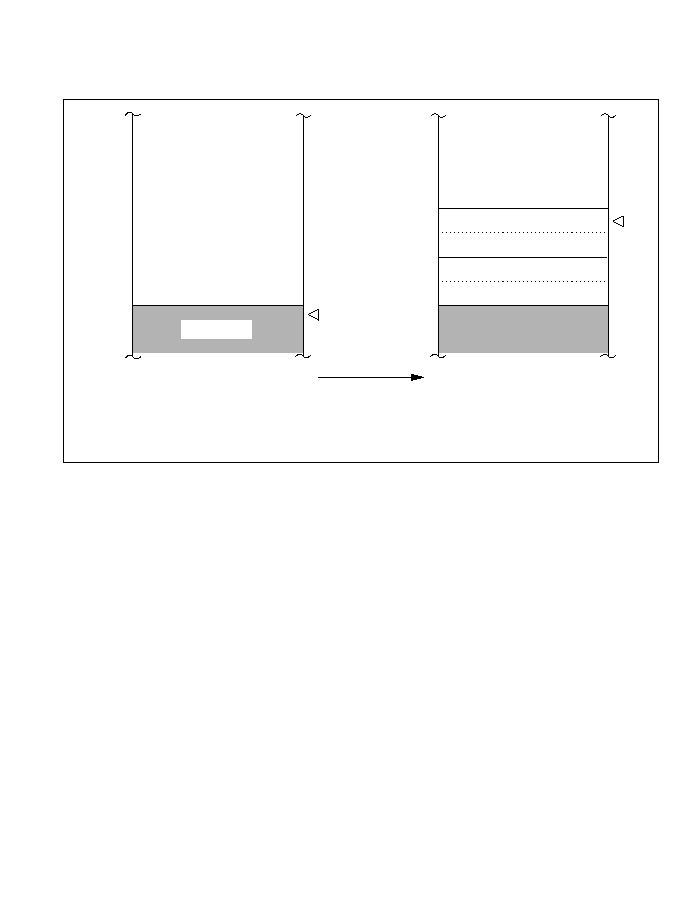
5.4.2 Stack Status after Interrupt Handling Sequence
Figure 5-3 (a) and (b) show the stack before and after the interrupt exception-handling sequence.
SP
Address
SP
2m ≠ 4
2m ≠ 3
2m ≠ 2
2m ≠ 1
2m
Address
2m ≠ 4
2m ≠ 3
2m ≠ 2
2m ≠ 1
2m
Upper 8 bits of SR
Lower 8 bits of SR
Upper 8 bits of PC
Lower 8 bits of PC
(After)
(Before)
Stack area
Save to stack
Notes:
1. PC: The address of the next instruction to be executed is saved.
2. Register saving and restoring must start at an even address (e.g 2m).
Figure 5-3 (a) Stack before and after Interrupt Exception-Handling
(Minimum Mode)
107

5.4.3 Timing of Interrupt Exception-Handling Sequence
Figure 5-4 shows the timing of the exception-handling sequence for an interrupt when the
program area and stack area are both in on-chip memory and the user-coded interrupt handling
routine starts at an even address.
5.5 Interrupts During Operation of the Data Transfer Controller
If an interrupt is requested during a DTC data transfer cycle, the interrupt is not accepted until the
data transfer cycle has been completed and the next instruction has been executed. This is true
even if the interrupt is an NMI. An example is shown below.
SP
Address
SP
2m ≠ 4
2m ≠ 3
2m ≠ 2
2m ≠ 1
2m
Address
2m ≠ 4
2m ≠ 3
2m ≠ 2
2m ≠ 1
2m
Upper 8 bits of SR
CP
Upper 8 bits of PC
Lower 8 bits of PC
(After)
(Before)
Stack area
Save to stack
Notes:
1. PC: The address of the next instruction to be executed is saved.
2. Register saving and restoring must start at an even address (e.g 2m).
2m ≠ 5
2m ≠ 6
2m ≠ 5
2m ≠ 6
Lower 8 bits of SR
Don't care
ADD.W R2, R0
MOV.W R0, @H'FF00
ADD.W @H' FF02,R0
Program flow
DTC interrupt request
Data transfer cycle request
NMI interrupt
After data transfer cycle, CPU executes next
instruction before starting exception handling
To NMI exception handling sequence
(Example)
Figure 5-3 (b) Stack before and after Interrupt Exception-Handling
(Maximum Mode)
108
(3)
Vector
address
SP - 4
SP - 2
(4)
Vector
SR
PC
(2)
(2)
(2)
(1)
(1)
(1)
NMI, IRQ
0
IRQ
1
¯
Interrupt
address
bus
Interrupt
data
bus (16 bits)
Interrupt
reset
signal
Interrupt
write
signal
Priority level
decision and wait
for end of
current instruction
Stack access
Internal
process-
ing cycle
Prefetch first
instruction of
interrupt-
handling routine
Start instruction
execution
Interrupt
accepted
(1) Instruction prefetch address (2) Instruction code (3) Starting address of interrupt-handling routine (4) Fi
rst instruction of interrupt-handling routine
Note:
This timing chart applies to the minimum mode when the program and stack areas are both in on-chip memory and the interrupt-han
dling routine starts
at an even address.
Figure 5-4 Interrupt Sequence (Minimum Mode, On-Chip Memory)
109
NMI, IRQ
0
IRQ
1
¯
Internal
address bus
Internal data
bus (16 bits)
Internal Read
signal
Internal Write
signal
Priority level
decision
and wait for
end of
current
instruction
(1) Instruction prefetch address
(2) Instruction code
(3) Starting address of interrupt-handling routine
(4) First instruction of interrupt-handling routine
Internal
processing
cycle
Stack access
Interrupt vector
Prefetch first instruction of
interrupt-handling routine
Start
instruction
execution
Note:
This timing chart applies to the maximum mode when the program and stack areas are both in external memory.
Instruction execution starts after interrupt vector fetch and 4-byte (4 bys cycles) instruction prefetch has been done.
(1)
(1)
SP ≠ 2
SP ≠ 1
SP ≠ 4
SP ≠ 3
SP ≠ 6
SP ≠ 5
Vector
Vector
address
address + 1
address + 2
address + 3
Vector
Vector
(3)
(2)
(2)
PC
H
PC
L
CP
SR
L
SR
H
don't
care
Vector
Vector
Vector
(4)
don't
care
Figure 5-5 Interrupt Sequence (Maximum Mode, External Memory)
110

5.6 Interrupt Response Time
Table 5-4 indicates the number of states that may elapse between the generation of an interrupt
request and the execution of the first instruction of the interrupt-handling routine, assuming that
the interrupt is not masked and not preempted by a higher-priority interrupt. Since word access is
performed to on-chip memory areas, fastest interrupt service can be obtained by placing the
program in on-chip ROM and the stack in on-chip RAM.
Table 5-4 Number of States before Interrupt Service
Note: m: Number of wait states inserted in external memory access.
Values in parentheses are for the LDM instruction.
Number of States
No.
Reason for Wait
Minimum Mode
Maximum Mode
1
Interrupt priority decision and comparison with
2 states
mask level in CPU status register
2
Maximum number of
Instruction is in on-chip
x
states to completion
memory
(x = 38 for LDM instruction specifying
of current instruction
all registers)
Instruction is in external
y
memory
(y = 74 + 16m for LDM instruction
specifying all registers)
3
Saving of PC and SR
Stack is in on-chip RAM
16
21
or PC, CP, and SR
Stack is in external memory
28 + 6m
41 + 10m
and instruction prefetch
Stack is in
Instruction is in on-chip
18 + x
23 + x
on-chip RAM
memory
(56)
(61)
Instruction is in external
18 + y
23 + y
Total
memory
(92 + 16m)
(97 + 16m)
Stack is in
Instruction is in on-chip
30 + 6m + x
43 + 10m + x
external RAM
memory
(68 + 6m)
(81 + 10m)
Instruction is in external
30 + 6m + y
43 + 10m + y
memory
(104 + 22m)
(117 + 26m)
111

Section 6 Data Transfer Controller
6.1 Overview
The H8/532 chip includes a data transfer controller (DTC) that can be started by designated
interrupts to transfer data from a source address to a destination address located in page 0. These
addresses include in particular the registers of the on-chip supporting modules and I/O ports.
Typical uses of the DTC are to change the setting of a control register of an on-chip supporting
module in response to an interrupt from that module, or to transfer data from memory to an I/O
port or the serial communication interface. Once set up, the transfer is interrupt-driven, so it
proceeds independently of program execution, although program execution temporarily stops
while each byte or word is being transferred.
6.1.1 Features
The main features of the DTC are listed below.
∑ The source address and destination address can be set anywhere in the 64k-byte address space
of page 0.
∑ The DTC can be programmed to transfer one byte or one word of data per interrupt.
∑ The DTC can be programmed to increment the source address and/or destination address after
each byte or word is transferred.
∑ After transferring a designated number of bytes or words, the DTC generates a CPU interrupt
with the vector of the interrupt source that started the DTC.
∑ This designated data transfer count can be set from 1 to 65,536 bytes or words.
6.1.2 Block Diagram
Figure 6-1 shows a block diagram of the DTC.
The four DTC control registers (DTMR, DTSR, DTDR, and DTCR) are invisible to the CPU, but
corresponding information is kept in a register information table in memory. A separate table is
maintained for each DTC interrupt type. When an interrupt requests DTC service, the DTC loads
its control registers from the table in memory, transfers the byte or word of data, and writes any
altered register information back to memory.
113

6.1.3 Register Configuration
The four DTC control registers are listed in table 6-1. These registers are not located in the
address space and cannot be written or read by the CPU. To set information in these registers, a
program must write the information in a table in memory from which it will be loaded by the
DTC.
Table 6-1 Internal Control Registers of the DTC
Name
Abbreviation
Read/Write
Data transfer mode register
DTMR
Disabled
Data transfer source address register
DTSR
Disabled
Data transfer destination address register
DTDR
Disabled
Data transfer count register
DTCR
Disabled
IRQ
0
IRQ
1
Internal data bus
DTC request
DTC
Interrupt controller
DTEA
DTEB
DTEC
DTED
DTMR
DTSR
DTDR
DTCR
DTMR:
DTSR:
DTDR:
DTCR:
DTEA to DTED:
DT Mode Register
DT Source Address Register
DT Destination Address Register
DT Count Register
DT Enable Register A to D
RAM
Register
information table
0
Register
information table
1
Figure 6-1 Block Diagram of Data Transfer Controller
114

Starting of the DTC is controlled by the four data transfer enable registers, which are located in
high addresses in page 0. Table 6-2 lists these registers.
Table 6-2 Data Transfer Enable Registers
Name
Abbreviation
Read/Write
Address
Initial Value
Data transfer
A
DTEA
R/W
H'FFF4
H'00
enable
B
DTEB
R/W
H'FFF5
H'00
register
C
DTEC
R/W
H'FFF6
H'00
D
DTED
R/W
H'FFF7
H'00
6.2 Register Descriptions
6.2.1 Data Transfer Mode Register (DTMR)
The data transfer mode register is a 16-bit register, the first three bits of which designate the data
size and specify whether to increment the source and destination addresses.
Bit 15--Sz (Size): This bit designates the size of the data transferred.
Bit 15
Sz
Description
0
Byte transfer
1
Word transfer* (two bytes at a time)
*
For word transfer, the source and destination addresses must be even addresses.
Bit 14--SI (Source Increment): This bit specifies whether to increment to source address.
Bit 14
SI
Description
0
Source address is not incremented.
1
1) If Sz = 0: Source address is incremented by +1 after each data transfer.
2) If Sz = 1: Source address is incremented by +2 after each data transfer.
Bit
15
14
13
12
11
10
9
8
7
6
5
4
3
2
1
0
Sz
SI
DI
--
--
--
--
--
--
--
--
--
--
--
--
--
Read/Write --
--
--
--
--
--
--
--
--
--
--
--
--
--
--
--
115

Bit 13--DI (Destination Increment): This bit specifies whether to increment to destination
address.
Bit 13
DI
Description
0
Destination address is not incremented.
1
1) If Sz = 0: Destination address is incremented by +1 after each data transfer.
2) If Sz = 1: Destination address is incremented by +2 after each data transfer.
Bits 12 to 0--Reserved Bits: These bits are reserved.
6.2.2 Data Transfer Source Address Register (DTSR)
The data transfer source register is a 16-bit register that designates the data transfer source
address. For word transfer this must be an even address. In the maximum mode, this address is
implicitly located in page 0.
6.2.3 Data Transfer Destination Register (DTDR)
The data transfer destination register is a 16-bit register that designates the data transfer
destination address. For word transfer this must be an even address. In the maximum mode, this
address is implicitly located in page 0.
6.2.4 Data Transfer Count Register (DTCR)
Bit
15
14
13
12
11
10
9
8
7
6
5
4
3
2
1
0
Read/Write --
--
--
--
--
--
--
--
--
--
--
--
--
--
--
--
Bit
15
14
13
12
11
10
9
8
7
6
5
4
3
2
1
0
Read/Write --
--
--
--
--
--
--
--
--
--
--
--
--
--
--
--
Bit
15
14
13
12
11
10
9
8
7
6
5
4
3
2
1
0
Read/Write --
--
--
--
--
--
--
--
--
--
--
--
--
--
--
--
116
The data transfer count register is a 16-bit register that counts the number of bytes or words of
data remaining to be transferred. The initial count can be set from 1 to 65,536. A register value of
0 designates an initial count of 65,536.
The data transfer count register is decremented automatically after each byte or word is
transferred. When its value reaches 0, indicating that the designated number of bytes or words
have been transferred, a CPU interrupt is generated with the vector of the interrupt that requested
the data transfer.
6.2.5 Data Transfer Enable Registers A to D (DTEA to DTED)
These four registers designate whether an interrupt starts the DTC. The bits in these registers are
assigned to interrupts as indicated in table 6-3. No bits are assigned to the NMI, FOVI, OVI, and
ERI interrupts, which cannot request data transfers.
Table 6-3 Assignment of Data Transfer Enable Registers
Note: Bits marked "--" should always be cleared to "0."
If the bit for a certain interrupt is set to "1," that interrupt is regarded as a request for DTC service.
If the bit is cleared to "0," the interrupt is regarded as a CPU interrupt request.
Only the 16 interrupts indicated in table 6-3 can request DTC service. DTE bits not assigned to
any interrupt (indicated by "--" in table 6-3) should be left cleared to "0."
Bit
7
6
5
4
3
2
1
0
Initial value
0
0
0
0
0
0
0
0
Read/Write
R/W
R/W
R/W
R/W
R/W
R/W
R/W
R/W
Interrupt Source
Interrupt Source
Register Module
Bits 7 to 4
Module
Bits 3 to 0
7
6
5
4
3
2
1
0
DTEA
IRQ
0
--
--
--
IRQ
0
IRQ
1
--
--
--
IRQ
1
DTEB
16-Bit FRT1
--
OCIB OCIA
ICI
16-Bit FRT2
--
OCIB OCIA
ICI
DTEC
16-Bit FRT3
--
OCIB OCIA
ICI
8-Bit Timer
--
--
CMIB CMIA
DTED
SCI
--
TXI
RXI
--
A/D converter
--
--
--
ADI
117

∑ Note on Timing of DTE Modifications: The interrupt controller requires two system clock (¯)
periods to determine the priority level of an interrupt. Accordingly, when an instruction modifies
a data transfer enable register, the new setting does not take effect until the third state after that
instruction has been executed.
6.3 Data Transfer Operation
6.3.1 Data Transfer Cycle
When started by an interrupt, the DTC executes the following data transfer cycle:
1. From the DTC vector table, the DTC reads the address at which the register information table
for that interrupt is located in memory.
2. The DTC loads the data transfer mode register and source address register from this table and
reads the data (one byte or word) from the source address.
3. If so specified in the mode register, the DTC increments the source address register and writes
the new source address back to the table in memory.
4. The DTC loads the data transfer destination address register and writes the byte or word of data
to the destination address.
5. If so specified in the mode register, the DTC increments the destination address register and
writes the new destination address back to the table in memory.
6. The DTC loads the data transfer count register from the table in memory, decrements the data
count, and writes the new count back to memory.
7. If the data transfer count is now 0, the DTC generates a CPU interrupt. The interrupt vector is
the vector of the interrupt type that started the DTC.
At an appropriate point during this procedure the DTC also clears the interrupt request by clearing
the corresponding flag bit in the status register of the on-chip supporting module to "0." (For
IRQ
0
or IRQ
1
, the DTC clears an internal latch.)
But the DTC does not clear the data transfer enable bit in the data transfer enable register. This
action, if necessary, must be taken by the user-coded interrupt-handling routine invoked at the end
of the transfer.
The data transfer cycle is shown in a flowchart in figure 6-2.
For the steps from the occurrence of the interrupt up to the start of the data transfer cycle, see
section 5.4.1, "Interrupt Handling Flow."
118
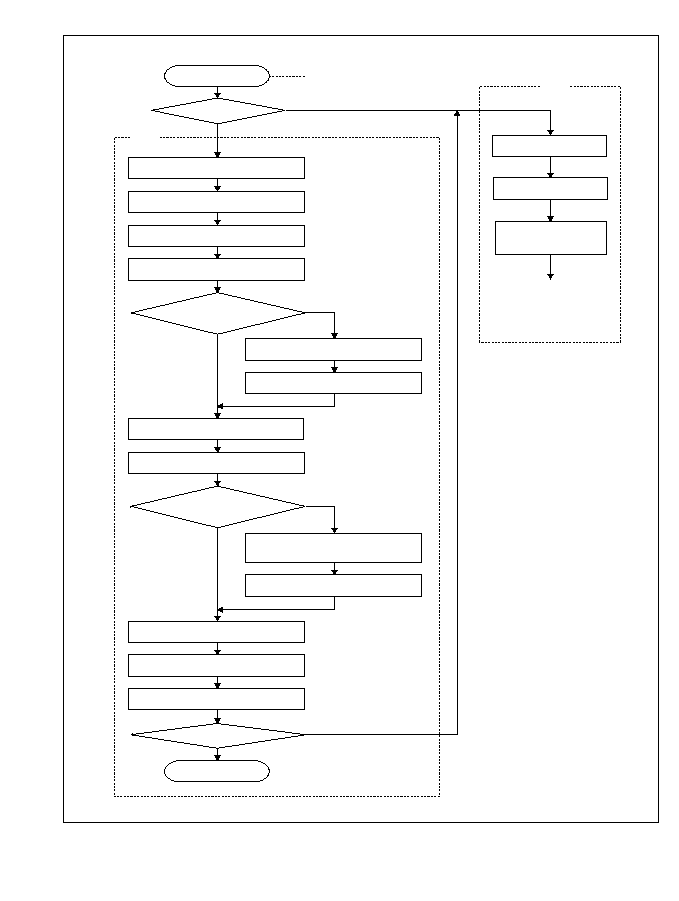
INT
Interrupt
DTC interrupt?
N
Y
DTC
Read DTC vector
Read transfer mode
Read source address
Read data
Source address
increment mode?
N
Y
Read destination address
Write data
Destination address
increment mode?
N
Y
Increment source address (+1 or +2)
Write source address
Write destination address
Increment destination address
(+1 or +2)
Read DTCR
DTCR DTCR
Write DTCR
DTCR = 0?
Y
N
DTC END
CPU
Save PC and SR
Read vector
Read address from
vector table
Start executing
interrupt-handling
routine at that
address.
Figure 6-2 Flowchart of Data Transfer Cycle
119
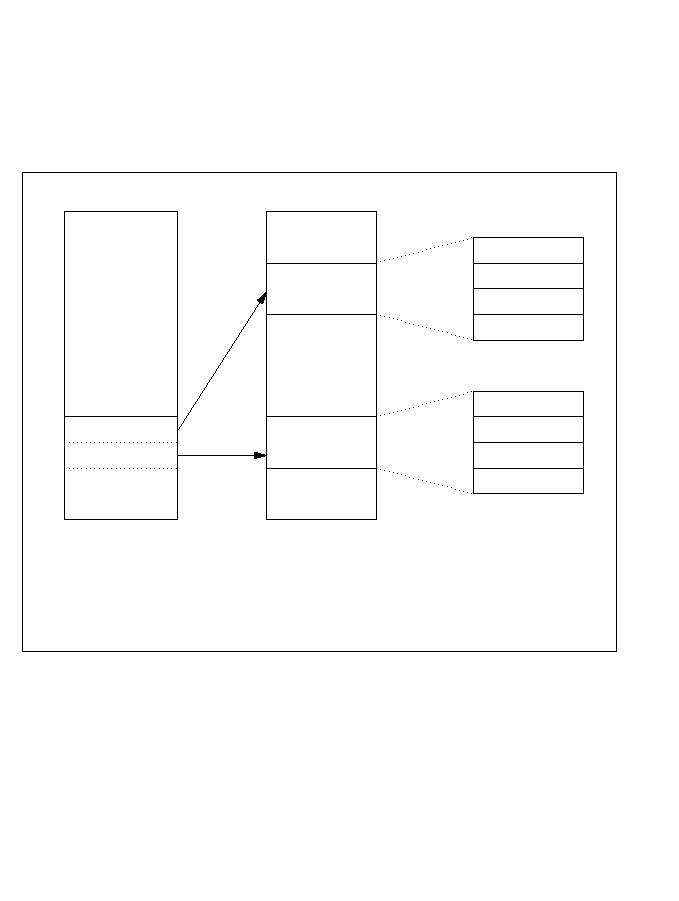
6.3.2 DTC Vector Table
The DTC vector table is located immediately following the exception vector table at the beginning
of page 0 in memory. For each interrupt that can request DTC service, the DTC vector table
provides a pointer to an address in memory where the table of DTC control register information
for that interrupt is stored. The register information tables can be placed in any available locations
in page 0.
In minimum mode, each entry in the DTC vector table consists of two bytes, pointing to an
address in page 0. In maximum mode, for compatibility reasons, each DTC vector table entry
consists of four bytes but the first two bytes are ignored; the last two bytes point to an address
which is implicitly assumed to be in page 0, regardless of the current page specifications.
Figure 6-4 shows one DTC vector table entry in minimum and maximum mode.
Vector table
Exception
vector table
TA
0
DTC vector
table
Register
information table
0
RAM
Register
information table
1
DTMR0
DTSR0
DTDR0
DTCR0
DTMR1
DTSR1
DTDR1
DTCR1
TA
1
TA
1
TA
0
ote: TA , TA ,... : Addresses of DTC register information tables in memory.
0
1
Note: TA
0
, TA
1
, ...: Addresses of DTC register information tables in memory.
In the normal case the register information tables are placed on a RAM. If the
software does not need to modify the register information (addresses are fixed and
transfer count is 1), it can be placed on ROM.
Figure 6-3 DTC Vector Table
120
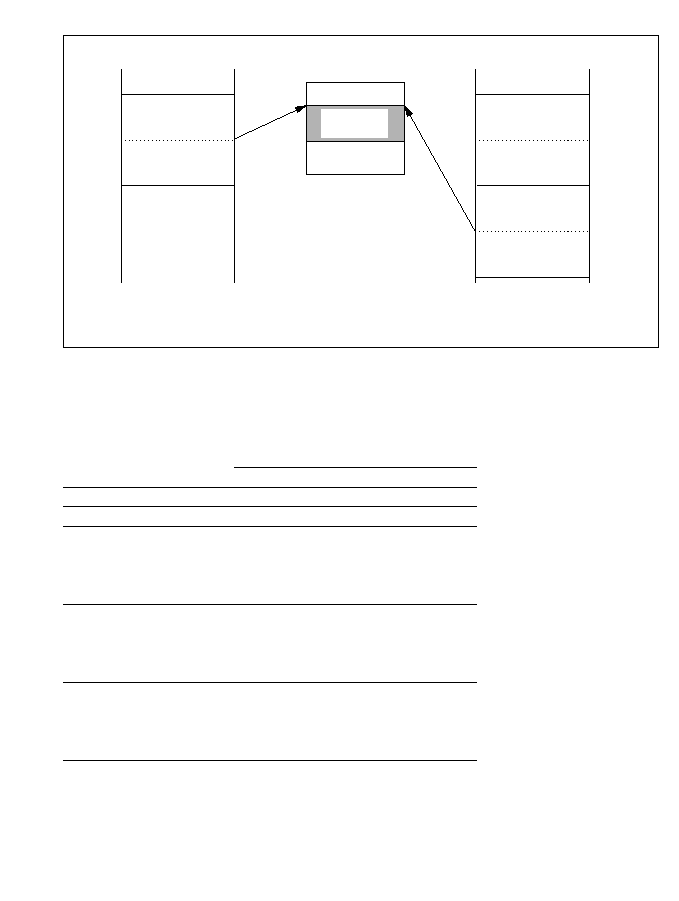
Table 6-4 lists the addresses of the entries in the DTC vector table for each interrupt.
Table 6-4 Addresses of DTC Vectors
DTC vector table
Address
m
m + 1
Address (H)
Address (L)
RAM
DTC vector table
Register
information
(1) Minimum mode
Address
2m*
2 m + 1*
Don't care
Don't care
(2) Maximum mode
2 m + 2
Address (H)
2 m + 3
Address (L)
* Address 2m and 2m + 1 are not accessed at vector read.
Address of DTC Vector
Interrupt
Minimum Mode
Maximum Mode
IRQ
0
H'0080 - H'0081
H'0100 - H'0103
IRQ
1
H'0082 - H'0083
H'0104 - H'0107
16-Bit
ICI
H'0088 - H'0089
H'0110 - H'0113
free-running
OCIA
H'008A - H'008B
H'0114 - H'0117
timer 1
OCIB
H'008C - H'008D
H'0118 - H'011B
(FRT1)
FOVI
--
--
16-Bit
ICI
H'0090 - H'0091
H'0120 - H'0123
free-running
OCIA
H'0092 - H'0093
H'0124 - H'0127
timer 2
OCIB
H'0094 - H'0095
H'0128 - H'012B
(FRT2)
FOVI
--
--
16-Bit
ICI
H'0098 - H'0099
H'0130 - H'0133
free-running
OCIA
H'009A - H'009B
H'0134 - H'0137
timer 3
OCIB
H'009C - H'009D
H'0138 - H'013B
(FRT3)
FOVI
--
--
Figure 6-4 DTC Vector Table Entry
121

Table 6-4 Addresses of DTC Vectors (cont)
6.3.3 Location of Register Information in Memory
For each interrupt, the DTC control register information is stored in four consecutive words in
memory in the order shown in figure 6-5.
6.3.4 Length of Data Transfer Cycle
Table 6-5 lists the number of states required per data transfer, assuming that the DTC control
register information is stored in on-chip RAM. This is the number of states required for loading
and saving the DTC control registers and transferring one byte or word of data. Two cases are
considered: a transfer between on-chip RAM and a register belonging to an I/O port or on-chip
supporting module (i.e., a register in the register field from addresses H'FF80 to H'FFFF); and a
transfer between such a register and external RAM.
Address of DTC Vector
Interrupt
Minimum Mode
Maximum Mode
8-Bit
CMIA
H'00A0 - H'00A1
H'0140 - H'0143
timer
CMIB
H'00A2 - H'00A3
H'0144 - H'0147
OVI
--
--
Serial
ERI
--
--
communication
RXI
H'00AA - H'00AB
H'0154 - H'0157
interface
TXI
H'00AC - H'00AD
H'0158 - H'015B
A/D converter
ADI
H'00B0 - H'00B1
H'0160 - H'0163
DTC vector table
TA
TA + 2
RAM
DTMR
DTSR
DTDR
DTCR
8 Bits
8 Bits
TA + 4
TA + 6
Mode register
Source address register
Destination address register
Count register
Figure 6-5 Order of Register Information
122

Table 6-5 Number of States per Data Transfer
Note: Numbers in the table are the number of states.
The values in table 6-5 are calculated from the formula:
N = 26 + 2
◊
SI + 2
◊
DI + M
S
+ M
D
Where M
S
and M
D
have the following meanings:
M
S
: Number of states for reading source data
M
D
: Number of states for writing destination data
The values of M
S
and M
D
depend on the data location as follows:
Byte or word data in on-chip RAM:
≥
2 states
Byte data in external RAM or register field:
≥
3 states
Word data in external RAM or register field:
≥
6 states
If the DTC control register information is stored in external RAM, 20 + 4
◊
SI + 4
◊
DI must be
added to the values in table 6-5.
The values given above do not include the time between the occurrence of the interrupt request
and the starting of the DTC. This time includes two states for the interrupt controller to check
priority and a variable wait until the end of the current CPU instruction. At maximum, this time
equals the sum of the values indicated for items No. 1 and 2 in table 6-6.
If the data transfer count is 0 at the end of a data transfer cycle, the number of states from the end
of the data transfer cycle until the first instruction of the user-coded interrupt-handling routine is
executed is the value given for item No. 3 in table 6-6.
Increment Mode
On-Chip RAM
Module or I/O
External RAM
Module or I/O
Source
Destina-
Register
Register
(SI)
tion (DI)
Byte Transfer
Word Transfer
Byte Transfer
Word Transfer
0
0
31
34
32
38
0
1
33
36
34
40
1
0
33
36
34
40
1
1
35
38
36
42
123

Table 6-6 Number of States before Interrupt Service
m: Number of wait states inserted in external memory access
6.4 Procedure for Using the DTC
A program that uses the DTC to transfer data must do the following:
1. Set the appropriate DTMR, DTSR, DTDR, and DTCR register information in the memory
location indicated in the DTC vector table.
2. Set the data transfer enable bit of the pertinent interrupt to "1," and set the priority of the
interrupt source (in the interrupt priority register) and the interrupt mask level (in the CPU
status register) so that the interrupt can be accepted.
3. Set the interrupt enable bit in the control register for the interrupt source. (For IRQ
0
and IRQ
1
,
the control register is the port 1 control register, P1CR.)
Following these preparations, the DTC will be started each time the interrupt occurs. When the
number of bytes or words designated by the DTCR value have been transferred, after transferring
the last byte or word, the DTC generates a CPU interrupt.
The user-coded interrupt-handling routine must take action to prepare for or disable further DTC
data transfer: by readjusting the data transfer count, for example, or clearing the interrupt enable
bit. If no action is taken, the next interrupt of the same type will start the DTC with an initial data
transfer count of 65,536.
Number of States
No. Reason for Wait
Minimum Mode
Maximum Mode
1
Interrupt priority decision and comparison with
2 states
mask level in CPU status register
2
Maximum number of
Instruction is in on-chip
38
states to completion
memory
(LDM instruction specifying all registers)
of current instruction
Instruction is in external
74 + 16m
memory
(LDM instruction specifying all registers)
3
Saving of PC and SR
Stack is in on-chip RAM
16
21
or PC, CP, and SR
and instruction prefetch Stack is in external memory 28 + 6m
41 + 10m
124

6.5 Example
Purpose: To receive 128 bytes of serial data via the serial communication interface.
Conditions:
∑ Operating mode: Minimum mode
∑ Received data are to be stored in consecutive addresses starting at H'FC00.
∑ DTC control register information for the RXI interrupt is stored at addresses H'FB80 to H'FB87.
∑ Accordingly, the DTC vector table contains H'FB at address H'00AA and H'80 at address
H'00AB.
∑ The desired interrupt mask level in the CPU status register is 4, and the desired SCI interrupt
priority level is 5.
Procedure
1. The user program sets DTC control register information in addresses H'FB80 to H'FB87 as
shown in table 6-7.
Table 6-7 DTC Control Register Information Set in RAM
2. The program sets the RI (SCI Receive Interrupt) bit in the data transfer enable register (bit 5 of
register DTED) to "1."
3. The program sets the interrupt mask in the CPU status register to 4, and the SCI interrupt
priority in bits 6 to 4 of interrupt priority register IPRD to 5.
4. The program sets the SCI to the appropriate receive mode, and sets the receive interrupt enable
(RIE) bit in the serial control register (SCR) to "1" to enable receive interrupts.
5. Thereafter, each time the SCI receives one byte of data, it requests an RXI interrupt, which the
interrupt controller directs toward the DTC. The DTC transfers the byte from the SCI's receive
data register (RDR) into RAM, and clears the interrupt request before ending.
Address
Register
Description
Value Set
Byte transfer
H'FB80
DTMR
Source address fixed
H'2000
Increment destination address
H'FB82
DTSR
Address of SCI receive data register
H'FFDD
H'FB84
DTDR
Address H'FC00
H'FC00
H'FB86
DTCR
Number of bytes to be received: 128
H'0080
125

6. When 128 bytes have been transferred (DTCR = 0), the DTC generates a CPU interrupt. The
interrupt type is RXI.
7. The user-coded RXI interrupt-handling routine processes the received data and disables further
data transfer (by clearing the RIE bit, for example).
Figure 6-6 shows the DTC vector table and data in RAM for this example.
Address
H'00AA
H'00AB
H'FB
H'80
DTC vector table
RAM
Address
H'FB80
H'FB81
H'20
H'00
H'FF
H'DD
H'FC
H'00
H'00
H'80
H'FB87
H'FC00
H'FC7F
SCI
Receive data 1
Receive data 2
Receive data 128
RDR
Transferred
by DTC
Mode
Source address
Destination address
Counter
Figure 6-6 Use of DTC to Receive Data via Serial Communication Interface
126

Section 7 Wait-State Controller
7.1 Overview
To simplify interfacing to low-speed external devices, the H8/532 has an on-chip wait-state
controller (WSC) that can insert wait states (T
W
) to prolong bus cycles.
The wait-state function can be used in CPU and DTC access cycles to external addresses. It is not
used in access to on-chip supporting modules. The T
W
states are inserted between the T
2
state
and T
3
state in the bus cycle. The number of wait states can be selected by a value set in the wait-
state control register (WCR), or by holding the WAIT pin Low for the required interval.
7.1.1 Features
The main features of the wait-state controller are:
∑ Selection of three operating modes
Programmable wait mode, pin wait mode, or pin auto-wait mode
∑ 0, 1, 2, or 3 wait states can be inserted.
And in the pin wait mode, 4 or more states can be inserted by holding the WAIT pin Low.
127
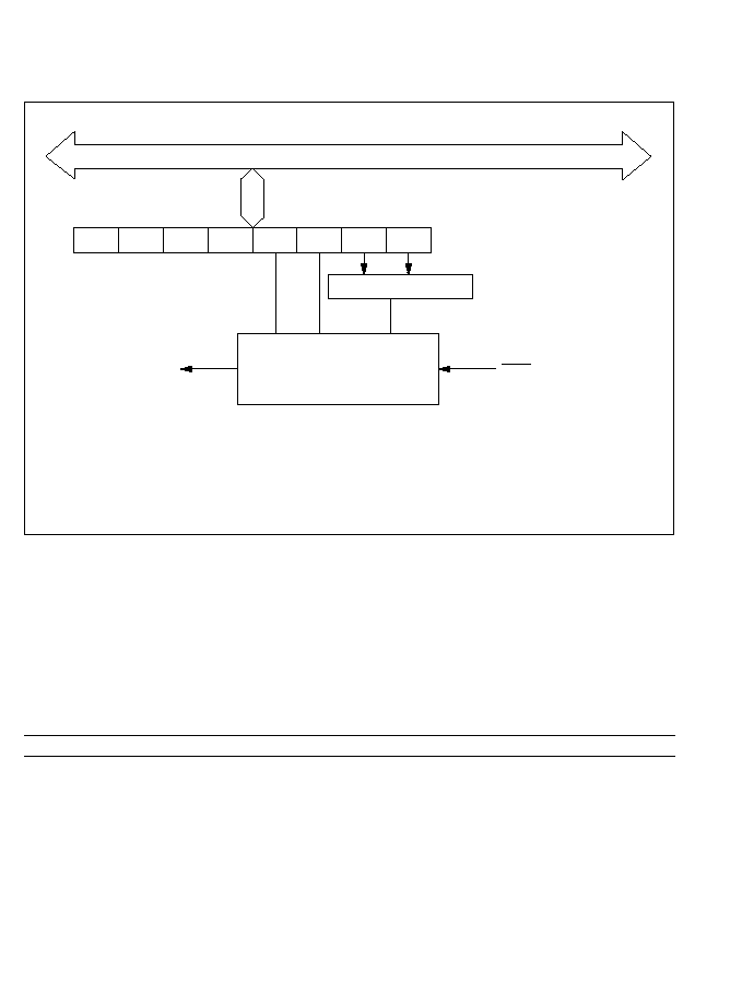
7.1.2 Block Diagram
Figure 7-1 shows a block diagram of the wait-state controller.
7.1.3 Register Configuration
The wait-state controller has one control register: the wait-state control register described in
table 7-1.
Table 7-1 Register Configuration
Name
Abbreviation
Read/Write
Initial Value
Address
Wait-state control register
WCR
R/W
H'F3
H'FFF8
Internal data bus
WAIT input
WCR:
WMS1, 0:
WC1, 0:
Control logic
WCR
--
--
--
--
WMS1 WMS0
WC1
WC0
Wait counter
WAIT request
Wait-state Control Register
Wait Mode Select 1, 0
Wait Count 1, 0
Figure 7-1 Block Diagram of Wait-State Controller
128

7.2 Wait-State Control Register
The wait-state control register (WCR) is an 8-bit register that specifies the wait mode and the
number of wait states to be inserted. A reset initializes the WCR to specify the programmable
wait mode with three wait states. The WCR is not initialized in the software standby mode.
Bits 7 to 4--Reserved: These bits cannot be modified and are always read as "1."
Bits 3 and 2--Wait Mode Select 1 and 0 (WMS1 and WMS0): These bits select the wait mode
as shown below.
Bits 1 and 0--Wait Count (WC1 and WC0): These bits specify the number of wait states to be
inserted.
Wait states are inserted only in bus cycles in which the CPU or DTC accesses an external address.
Bit
7
6
5
4
3
2
1
0
--
--
--
--
WMS1
WMS0
WC1
WC0
Initial value
1
1
1
1
0
0
1
1
Read/Write
--
--
--
--
R/W
R/W
R/W
R/W
Bit 3
Bit 2
WMS1
WMS0
Description
0
0
Programmable wait mode
(Initial value)
0
1
No wait states are inserted, regardless of the wait count.
1
0
Pin wait mode
1
1
Pin auto-wait mode
Bit 1
Bit 0
WC1
WC0
Description
0
0
No wait states are inserted, except in pin wait mode.
0
1
1 Wait state in inserted.
1
0
2 Wait states are inserted.
1
1
3 Wait states are inserted.
(Initial value)
129

7.3 Operation in Each Wait Mode
Table 7-2 summarizes the operation of the three wait modes.
Table 7-2 Wait Modes
WAIT
Insertion
Number of Wait
Mode
Pin Function
Conditions
States Inserted
Programmable
Disabled
Inserted on access to 1 to 3 wait states are inserted, as
wait mode
an off-chip address
specified by bits WC0 and WC1.
WMS1 = "0"
WMS0 = "0"
Pin wait mode
Enabled
Inserted on access to 0 to 3 wait states are inserted, as
WMS1 = "1"
an off-chip address
specified by bits WC0 and WC1,
WMS0 = "0"
plus additional wait states while the
WAIT pin is held Low.
Pin auto-wait
Enabled
Inserted on access to 1 to 3 wait states are inserted, as
mode
an off-chip address if
specified by bits WC0 and WC1.
WMS1 = "1"
the WAIT pin is Low
WMS0 = "1"
7.3.1 Programmable Wait Mode
The programmable wait mode is selected when WMS1 = "0" and WMS0 = "0."
Whenever the CPU or DTC accesses an off-chip address, the number of wait states set in bits
WC1 and WC0 are inserted. The WAIT pin is not used for wait control; it is available as an I/O
pin.
130
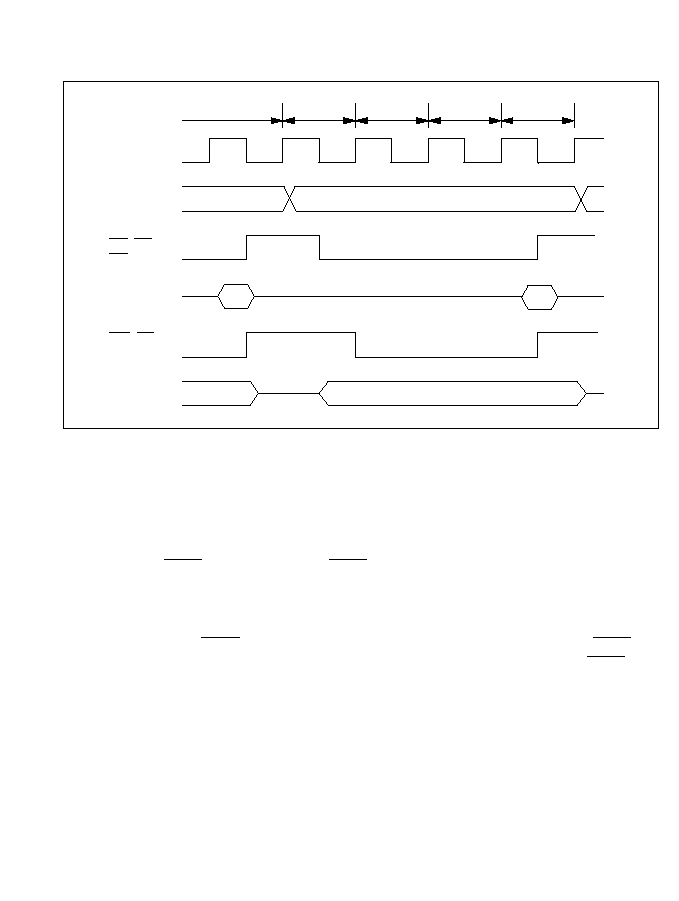
Figure 7-2 shows the timing of the operation in this mode when the wait count is 1 (WC1 = "0,"
WC0 = "1").
7.3.2 Pin Wait Mode
The pin wait mode is selected when WMS1 = "1" and WMS0 = "0."
In this mode the WAIT function of the P1
4
/WAIT pin is used automatically.
The number of wait states indicated by bits WC1 and WC0 are inserted into any bus cycle in
which the CPU or DTC accesses an off-chip address. In addition, wait states continue to be
inserted as long as the WAIT pin is held low. In particular, if the wait count is 0 but the WAIT pin
is Low at the rising edge of the ¯ clock in the T
2
state, wait states are inserted until the WAIT pin
goes High.
This mode is useful for inserting four or more wait states, or when different external devices
require different numbers of wait states.
T
RD, AS,
DS (Read)
D ≠D
7
0
A ≠A
19
0
¯
D ≠D
7
0
WR, DS
(Write)
Read data
Off-chip address
Read data
Write data
2
state or T
3
T
1
T
2
T
W
T
3
Figure 7-2 Programmable Wait Mode
131

Figure 7-3 shows the timing of the operation in this mode when the wait count is 1 (WC1 = "0,"
WC0 = "1") and the WAIT pin is held Low to insert one additional wait state.
RD, AS,
DS (Read)
D ≠D
7
0
¯
D ≠D
7
0
WR, DS
(Write)
A ≠A
19
0
WAIT pin
Off-chip address
Write data
Read data
T
2
T
1
T
W
Wait
count
T
W
T
3
WAIT
pin
*
*
*
The arrowheads indicate the times at which the WAIT pin is sampled.
Figure 7-3 Pin Wait Mode
132
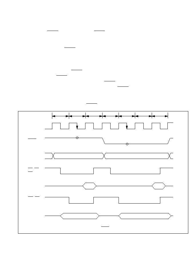
7.3.3 Pin Auto-Wait Mode
The pin auto-wait mode is selected when WMS1 = "1" and WMS0 = "1."
In this mode the WAIT function of the P1
4
/WAIT pin is used automatically.
In this mode, the number of wait states indicated by bits WC1 and WC0 are inserted, but only if
there is a Low input at the WAIT pin.
Figure 7-4 shows the timing of this operation when the wait count is 1.
In the pin auto-wait mode, the WAIT pin is sampled only once, on the falling edge of the ¯ clock
in the T
2
state. If the WAIT pin is Low at this time, the wait-state controller inserts the number of
wait states indicated by bits WC1 and WC0. The WAIT pin is not sampled during the Tw and T
3
states, so no additional wait states are inserted even if the WAIT pin continues to be held Low.
This mode offers a simple way to interface a low-speed device: the wait states can be inserted by
routing an address decode signal to the WAIT pin.
RD, AS,
DS (Read)
D ≠D
7
0
¯
D ≠D
7
0
WR, DS
(Write)
A ≠A
19
0
WAIT
External address
External address
Read data
Read data
Write data
Write data
*
*
T
1
T
2
T
3
T
1
T
2
T
3
T
W
*
The arrowheads indicate the times at which the WAIT pin is sampled.
Figure 7-4 Pin Auto-Wait Mode
133

Section 8 Clock Pulse Generator
8.1 Overview
The H8/532 chip has a built-in clock pulse generator (CPG) consisting of an oscillator circuit, a
system (¯) clock divider, an E clock divider, and a group of prescalers. The prescalers generate
clock signals for the on-chip supporting modules.
8.1.1 Block Diagram
8.2 Oscillator Circuit
If an external crystal is connected across the EXTAL and XTAL pins, the on-chip oscillator circuit
generates a clock signal for the system clock divider. Alternatively, an external clock signal can
be applied to the EXTAL pin.
Connecting an External Crystal
(1) Circuit Configuration: An external crystal can be connected as in the example in figure 8-2.
An AT-cut parallel resonating crystal should be used.
XTAL
EXTAL
¯
E
¯/2 to ¯/4096
Oscillator
circuit
Divider
˜ 2
Divider
˜ 8
CPG
Prescaler
Figure 8-1 Block Diagram of Clock Pulse Generator
135

(2) Crystal Oscillator: The external crystal should have the characteristics listed in table 8-1.
Table 8-1 External Crystal Parameters
(3) Note on Board Design: When an external crystal is connected, other signal lines should be
kept away from the crystal circuit to prevent induction from interfering with correct
oscillation. See figure 8-4.
When the board is designed, the crystal and its load capacitors should be placed as close as
possible to the XTAL and EXTAL pins.
EXTAL
C
XTAL
L1
C
L2
C =C =10 to 22pF
L1
L2
C
L
XTAL
EXTAL
L
R
S
C
0
AT-cut parallel resonating crystal
Frequency (MHz)
2
4
8
12
16
20
Rs max (
)
500
120
60
40
30
20
C
0
(pF)
7pF max
Figure 8-2 Connection of Crystal Oscillator (Example)
Figure 8-3 Crystal Oscillator Equivalent Circuit
136

Input of External Clock Signal
(1) Circuit Configuration: An external clock signal can be input at the EXTAL and XTAL pins
as shown in the example in figure 8-5.
Note: When using make ROM, an external clock can be input at the EXTAL pin while leaving
the XTAL pin open. Also when using ZTAT, an external clock under 16 MHz can be input
at the EXTAL pin while leaving the XTAL pin open.
C
L2
C
L1
Not allowed
Signal A
Signal B
H8/532
XTAL
EXTAL
External clock input
74HC04
EXTAL
XTAL
Figure 8-4 Notes on Board Design around External Crystal
Figure 8-5 External Clock Input (Example)
137

(2) External Clock Input
Frequency
Double the system clock (¯) frequency
Duty factor
45% to 55%
8.3 System Clock Divider
The system clock divider divides the crystal oscillator or external clock frequency (fosc) by 2 to
create the ¯ clock.
An E clock signal is created by dividing the ¯ clock by 8. The E clock is used for interfacing to E
clock based devices.
Figure 8-6 shows the phase relationship of the E clock to the ¯ clock.
E
¯
E
Figure 8-6 Phase Relationship of ¯ Clock and E Clock
138

Section 9 I/O Ports
9.1 Overview
The H8/532 has nine ports. Ports 1, 3, 4, 5, 7, and 9 are eight-bit input/output ports. Port 2 is a
five-bit input/output port. Port 6 is a four-bit input/output port. Port 8 is an eight-bit input-only
port. Table 9-1 summarizes the functions of each port.
Input and output are memory-mapped. The CPU views each port as a data register (DR) located
in the register field at the high end of page 0 of the address space. Each port (except port 8) also
has a data direction register (DDR) which determines which pins are used for input and which for
output. Port 1 has an additional control register (P1CR) for enabling and disabling IRQ
0
and
IRQ
1
and setting other controls.
To read data from an I/O port, the CPU selects input in the data direction register and reads the
data register. This causes the input logic level at the pin to be placed directly on the internal data
bus. There is no intervening input latch.
To send data to an output port, the CPU selects output in the data direction register and writes the
desired data in the data register, causing the data to be held in a latch. The latch output drives the
pin through a buffer amplifier. If the CPU reads the data register of an output port, it obtains the
data held in the latch rather than the actual level of the pin.
As table 9-1 indicates, all of the I/O port pins have dual functions. For example, pin 7 of port 1
can be used either as a general-purpose I/O pin (P1
7
), or for output of the TMO signal from the
on-chip 8-bit timer. The function is determined by the MCU operating mode, or by a value set in
a control register.
Outputs from ports 1 to 6 can drive one TTL load and a 90pF capacitive load. Outputs from ports
7 and 9 can drive one TTL load and a 30pF capacitive load.
Outputs from ports 1 to 7 and 9 can also drive a Darlington transistor pair. Outputs from port 4
can drive a light-emitting diode (with 10mA current sink). Ports 5 and 6 have built-in MOS pull-
ups for each input. Port 7 has Schmitt inputs.
Schematic diagrams of the I/O port circuits are shown in appendix C.
139

Table 9-1 Input/Output Port Summary
Expanded Modes
Single-Chip Mode
Port
Description
Pins
Mode 1 Mode 2 Mode 3 Mode 4
(Mode 7)
Port 1 8-Bit input/output P1
7
/ TMO
These input/output pins double as and
P1
6
/ IRQ
1
inputs and as IRQ
0
and IRQ
1
input and
P1
5
/ IRQ
0
output pin (TMO) for the 8-bit timer.
P1
4
/ WAIT These pins function as WAIT, BREQ,
Input/output
P1
3
/ BREQ and BACK when necessary control-
port
P1
2
/ BACK register bits are set to "1."
P1
1
/ E
These pins function as input pins or as
P1
0
/ ¯
clock (E, ¯) output pins, depending on
the data direction register setting.
Port 2 5-Bit input/output P2
4
/ WR
Bus control signal outputs
Input/output
port
P2
3
/ RD
(WR, RD, DS, R/W, AS)
port
P2
2
/ DS
P2
1
/ R/W
P2
0
/ AS
Port 3 8-Bit input/output P3
7
- P3
0
/
Data bus (D
7
≠ D
0
)
Input/output
port
D
7
≠ D
0
port
Port 4 8-Bit input/output P4
7
≠ P4
0
/ Low address bits (A
7
≠ A
0
)
Input/output
port
A
7
≠ A
0
port
Can drive a LED
Port 5 8-Bit input/output P5
7
≠ P5
0
/ High
High
High
High
Input/output
port
A
15
≠ A
8
address address address address
port
Built-in input
bus
bus if
bus
bus if
pull-up (MOS)
(A
15
≠
DDR is
(A
15
≠
DDR is
A
8
)
set to "1" A
8
)
set to "1"
Port 6 4-Bit input/output P6
3
≠P6
0
/
Input/output port Page
Page
Input/output
port
A
19
≠ A
16
address address
port
Built-in input
bus
bus if DDR
pull-up (MOS)
(A
19
≠
is set to "1,"
A
16
)
input port if
DDR is set
to "0"
140

Table 9-1 Input/Output Port Summary (cont)
Expanded Modes
Single-Chip Mode
Port
Description
Pins
Mode 1 Mode 2 Mode 3 Mode 4
(Mode 7)
Port 7 8-Bit input/output P7
7
/ FTOA
1
Input/output for free-running timers 1,
port
P7
6
/ FTOB
3
/ 2 and 3 (FTI
1
to FTI
3
, FTCI
1
to FTCI
3
,
(Schmitt inputs)
FTCI
3
FTOB
1
to FTOB
3
, FTOA
1
),input for
P7
5
/ FTOB
2
/ 8-bit timer input (TMCI, TMRI), and 8-bit
FTCI
2
input/output port
P7
4
/ FTOB
1
/ (P7
7
to P7
0
)
FTCI
1
/
P7
3
/ FTI
3
TMRI
P7
2
/ FTI
2
P7
1
/ FTI
1
P7
0
/ TMCI
Port 8 8-Bit input port
P8
0
- P8
7
Analog input pins for A/D converter, and
AN
7
≠ AN
0
8-bit input port
Port 9 8-Bit input/output P9
7
/ SCK
Output for free-running timers 2 and 3
port
P9
6
/ RXD
(FTOA
2
, FTOA
3
), PWM timer output
P9
5
/ TXD
(PW
1
, PW
2
, PW
3
), serial communication
P9
4
/ PW
3
interface (SCI) input/output (TXD, RXD,
P9
3
/ PW
2
SCK), and 8-bit input/output port
P9
2
/ PW
1
P9
1
/ FTOA
3
P9
0
/ FTOA
2
141
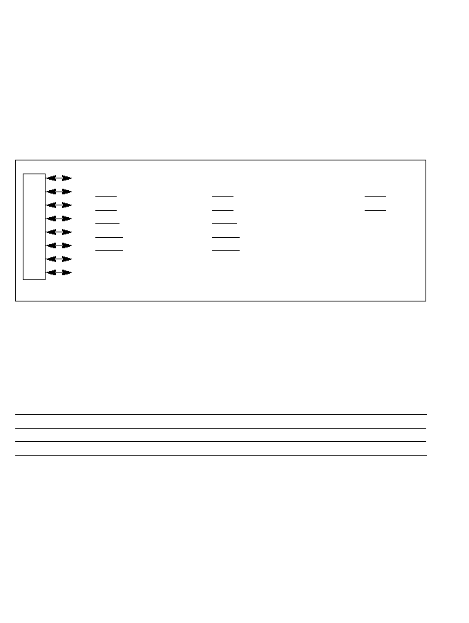
9.2 Port 1
9.2.1 Overview
Port 1 is an 8-bit input/output port with the pin configuration shown in figure 9-1. All pins have
dual functions, except that in the single-chip mode pins 4, 3, and 2 do not have the WAIT, BREQ,
and BACK functions. (because the CPU does not access an external bus.)
Outputs from port 1 can drive one TTL load and a 90pF capacitive load. They can also drive a
Darlington transistor pair.
9.2.2 Port 1 Registers
Register Configuration: Table 9-2 lists the registers of port 1.
Table 9-2 Port 1 Registers
Name
Abbreviation
Read/Write
Initial Value
Address
Port 1 data direction register
P1DDR
W
H'03
H'FF80
Port 1 data register
P1DR
R/W
*
1
Undetermined
*
2
H'FF82
Port 1 control register
P1CR
R/W
H'87
H'FFFC
*
1 Bits 1 and 0 are read-only.
*
2 Bits 1 and 0 are undetermined. Other bits are initialized to "0."
Pin
Expanded Modes
Single-Chip Mode
P1
7
/ TMO
P1
7
(input/output) / TMO (output)
P1
7
(input/output) / TMO (output)
P1
6
/ IRQ
1
P1
6
(input/output) / IRQ
1
(input)
P1
6
(input/output) / IRQ
1
(input)
P1
5
/ IRQ
0
P1
5
(input/output) / IRQ
0
(input)
P1
5
(input/output) / IRQ
0
(input)
Port
P1
4
/ WAIT
P1
4
(input/output) / WAIT (input)
P1
4
(input/output)
1
P1
3
/ BREQ P1
3
(input/output) / BREQ (input)
P1
3
(input/output)
P1
2
/ BACK
P1
2
(input/output) / BACK (output)
P1
2
(input/output)
P1
1
/ E
P1
1
(input) / E (output)
P1
1
(input) / E (output)
P1
0
/ ¯
P1
0
(input) / ¯ (output)
P1
0
(input) / ¯ (output)
Figure 9-1 Pin Functions of Port 1
142

1. Port 1 Data Direction Register (P1DDR)--H'FF80
P1DDR is an 8-bit register that selects the direction of each pin in port 1. A pin functions as an
output pin if the corresponding bit in P1DDR is set to "1," and as an input pin if the bit is cleared
to "0."
P1DDR can be written but not read. An attempt to read this register does not cause an error, but
all bits are read as "1," regardless of their true values.
A reset initializes P1DDR to H'03, so that pins P1
1
and P1
0
carry clock outputs and the other pins
are set for input. In the hardware standby mode, P1DDR is cleared to H'00, stopping the clock
outputs. P1DDR is not initialized in the software standby mode, so if a P1DDR bit is set to "1"
when the chip enters the software standby mode, the corresponding pin continues to output the
value in the port 1 data register (or the ¯ or E clock).
2. Port 1 Data Register (P1DR)--H'FF82
P1DR is an 8-bit register containing the data for pins P1
7
to P1
0
. When the CPU reads P1DR, for
output pins it reads the value in the P1DR latch, but for input pins, it obtains the pin status directly.
Note that when pins P1
1
and P1
0
are used for output, they output the clock signals (¯ and E), not
the contents of P1DR. If the CPU reads Pl
1
and Pl
0
(when Pl
1
DDR = Pl
0
DDR = 1), it obtains the
clock values at the current instant.
3. Port 1 Control Register (P1CR)--H'FFFC
Bit
7
6
5
4
3
2
1
0
P1
7
DDR P1
6
DDR P1
5
DDR P1
4
DDR P1
3
DDR P1
2
DDR P1
1
DDR P1
0
DDR
Initial value
0
0
0
0
0
0
1
1
Read/Write
W
W
W
W
W
W
W
W
Bit
7
6
5
4
3
2
1
0
P1
7
P1
6
P1
5
P1
4
P1
3
P1
2
P1
1
P1
0
Initial value
0
0
0
0
0
0
--
--
Read/Write
R/W
R/W
R/W
R/W
R/W
R/W
R
R
Bit
7
6
5
4
3
2
1
0
--
IRQ
1
E
IRQ
0
E
NMIEG
BRLE
--
--
--
Initial value
1
0
0
0
0
1
1
1
Read/Write
--
R/W
R/W
R/W
R/W
--
--
--
143

P1CR selects the functions of four of the port 1 pins. It also selects the input edge of the NMI pin.
At a reset and in the hardware standby mode, P1CR is initialized to H'87. It is not initialized in
the software standby mode.
Bit 7--Reserved: This bit cannot be modified and is always read as "1."
Bit 6--Interrupt Request 1 Enable (IRQ
1
E): This bit selects the function of pin P1
6
.
Bit 6
IRQ
1
E
Description
0
P1
6
functions as an input/output pin.
(Initial value)
1
P1
6
functions as the IRQ
1
input pin, regardless of the value set in P1
6
DDR. (However,
the CPU can still read the pin status by reading P1DR.)
Bit 5--Interrupt Request 0 Enable (IRQ
0
E): This bit selects the function of pin P1
5
.
Bit 5
IRQ
0
E
Description
0
P1
5
functions as an input/output pin.
(Initial value)
1
P1
5
functions as the IRQ
0
input pin, regardless of the value set in P1
5
DDR. (However,
the CPU can still read the pin status by reading P1DR.)
Bit 4--Nonmaskable Interrupt Edge (NMIEG): This bit selects the input edge of the NMI pin.
It is not related to port 0.
Bit 4
NMIEG
Description
0
A nonmaskable interrupt is generated on the falling edge
(Initial value)
of the input at the NMI pin.
1
A nonmaskable interrupt is generated on the rising edge
of the input at the NMI pin.
Bit 3--Bus Release Enable (BRLE): This bit selects the functions of pins P1
2
and P1
3
. It is
valid only in the expanded modes (modes 1, 2, 3, and 4). In the single-chip mode, pins P1
2
and
P1
3
function as input/output pins regardless of the value of the BRLE bit.
144
Bit 3
BRLE
Description
0
P1
3
and P1
2
function as input/output pins.
(Initial value)
1
P1
3
functions as the input pin. P1
2
functions as the output pin.
Bits 2 to 0--Reserved: These bits cannot be modified and are always read as "1."
9.2.3 Pin Functions in Each Mode
Port 1 operates differently in the expanded modes (modes 1, 2, 3, and 4) and the single-chip mode
(mode 7). Table 9-3 explains how the pin functions are selected in the expanded mode. Table 9-4
explains how the pin functions are selected in the single-chip mode.
Table 9-3 Port 1 Pin Functions in Expanded Modes
Pin
Functions and How they are Selected
P1
7
/ TMO The function depends on output select bits 3 to 0 (OS3 to OS0) of the 8-bit timer
control/status register (TCSR) and on the P1
7
DDR bit as follows:
OS3 to OS0
All four bits are "0"
At least one bit is "1"
P1
7
DDR
0
1
0
1
Pin function
P1
7
input
P1
7
output
TMO output
P1
6
/ IRQ
1
The function depends on the IRQ
1
E bit and the P1
6
DDR bit as follows:
IRQ
1
E
0
1
P1
6
DDR
0
1
0
1
Pin function
P1
6
input
P1
6
output
IRQ
1
input
P1
5
/ IRQ
0
The function depends on the IRQ
0
E bit and the P1
5
DDR bit as follows:
IRQ
0
E
0
1
P1
5
DDR
0
1
0
1
Pin function
P1
5
input
P1
5
output
IRQ
0
input
145

Table 9-3 Port 1 Pin Functions in Expanded Modes (cont)
Pin
Functions and How they are Selected
P1
4
/ WAIT
The function depends on the wait mode select 1 bit (WMS1) of the wait-state control
register (WCR) and the P1
4
DDR bit as follows:
WMS1
0
1
P1
4
DDR
0
1
0
1
Pin function
P1
4
input
P1
4
output
WAIT input
P1
3
/ BREQ
The function depends on the BRLE bit and the P1
3
DDR bit as follows:
BRLE
0
1
P1
3
DDR
0
1
0
1
Pin function
P1
3
input
P1
3
output
BREQ input
P1
2
/ BACK
The function depends on the BRLE bit and the P1
2
DDR bit as follows:
BRLE
0
1
P1
2
DDR
0
1
0
1
Pin function
P1
2
input
P1
2
output
BACK input
P1
1
/ E
P1
1
DDR
0
1
Pin function
Input
E clock output
P1
0
/ ¯
P1
0
DDR
0
1
Pin function
Input
¯ clock output
146
Table 9-4 Port 1 Pin Functions in Single-Chip Modes
Pin
Selection of Pin Functions
P1
7
/ TMO
The function depends on output select bits 3 to 0 (OS3 to OS0) of the 8-bit timer
control/status register (TCSR) and on the P1
7
DDR bit as follows:
OS3 to OS0
All four bits are "0"
At least one bit is "1"
P1
7
DDR
0
1
0
1
Pin function
P1
7
input
P1
7
output
TMO output
P1
6
/ IRQ
1
The function depends on the IRQ
1
E bit and the P1
6
DDR bit as follows:
IRQ
1
E
0
1
P1
6
DDR
0
1
0
1
Pin function
P1
6
input
P1
6
output
IRQ
1
input
P1
5
/ IRQ
0
The function depends on the IRQ
0
E bit and the P1
5
DDR bit as follows:
IRQ
0
E
0
1
P1
5
DDR
0
1
0
1
Pin function
P1
5
input
P1
5
output
IRQ
0
input
P1
4
P1
4
DDR
0
1
Pin function
Input
Output
P1
3
P1
3
DDR
0
1
Pin function
Input
Output
147

Table 9-4 Port 1 Pin Functions in Single-Chip Modes (cont)
Pin
Selection of Pin Functions
P1
2
P1
2
DDR
0
1
Pin function
Input
Output
P1
1
/ E
P1
1
DDR
0
1
Pin function
Input
E clock output
P1
0
/ ¯
P1
0
DDR
0
1
Pin function
Input
¯ clock output
9.3 Port 2
9.3.1 Overview
Port 2 is a five-bit input/output port with the pin configuration shown in figure 9-2. It functions as
an input/output port only in the single-chip mode. In the expanded modes it is used for output of
bus control signals.
Outputs from port 2 can drive one TTL load and a 90pF capacitive load. They can also drive a
Darlington transistor pair.
Pin
Expanded Modes
Single-Chip Mode
P2
4
/ WR
WR (output)
P2
4
(input/output)
Port
P2
3
/ RD
RD (output)
P2
3
(input/output)
2
P2
2
/ DS
DS (output)
P2
2
(input/output)
P2
1
/ R/W
R/W (output)
P2
1
(input/output)
P2
0
/ AS
AS (output)
P2
0
(input/output)
Figure 9-2 Pin Functions of Port 2
148

9.3.2 Port 2 Registers
Register Configuration: Table 9-5 lists the registers of port 2.
Table 9-5 Port 2 Registers
Name
Abbreviation
Read/Write
Initial Value
Address
Port 2 data direction register
P2DDR
W
H'E0
H'FF81
Port 2 data register
P2DR
R/W
H'E0
H'FF83
1. Port 2 Data Direction Register (P2DDR)--H'FF81
P2DDR is an 8-bit register that selects the direction of each pin in port 2.
Single-Chip Mode: A pin functions as an output pin if the corresponding bit in P2DDR is set
to "1," and as an input pin if the bit is cleared to "0."
Bits 4 to 0 can be written but not read. An attempt to read this register does not cause an error, but
all bits are read as "1," regardless of their true values.
Bits 7 to 5 are reserved. They cannot be modified and are always read as "1."
At a reset and in the hardware standby mode, P2DDR is initialized to H'E0, making all five pins
input pins. P2DDR is not initialized in the software standby mode, so if a P2DDR bit is set to "1"
when the chip enters the software standby mode, the corresponding pin continues to output the
value in the port 2 data register.
Expanded Modes: All bits of P2DDR are fixed at "1" and cannot be modified.
Bit
7
6
5
4
3
2
1
0
--
--
--
P2
4
DDR P2
3
DDR P2
2
DDR P2
1
DDR P2
0
DDR
Initial value
1
1
1
0
0
0
0
0
Read/Write
--
--
--
W
W
W
W
W
149
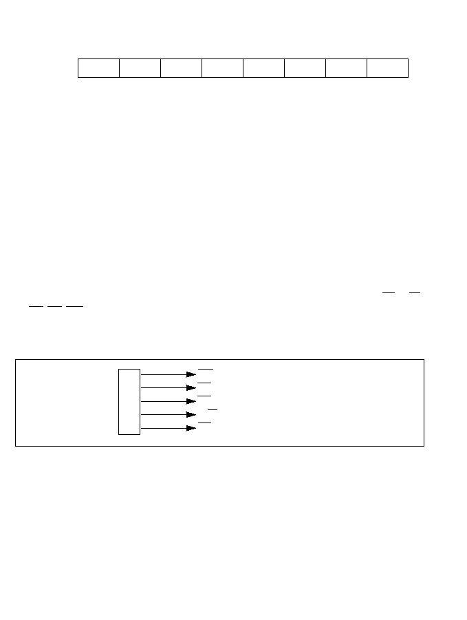
2. Port 2 Data Register (P2DR)--H'FF83
P2DR is an 8-bit register containing the data for pins P2
4
to P2
0
.
Bits 7 to 5 are reserved. They cannot be modified and are always read as "1."
When the CPU reads P2DR, for output pins it reads the value in the P2DR latch, but for input
pins, it obtains the pin status directly.
9.3.3 Pin Functions in Each Mode
Port 2 has different functions in the expanded modes (modes 1, 2, 3, 4) and the single-chip mode
(mode 7). Separate descriptions are given below.
Pin Functions in Expanded Modes: In the expanded modes (modes 1, 2, 3, and 4), all pins of
P2DDR is automatically set to "1" for output. Port 2 outputs the bus control signals (AS, R/W,
DS, RD, WR).
Figure 9-3 shows the pin functions in the expanded modes.
Bit
7
6
5
4
3
2
1
0
--
--
--
P2
4
P2
3
P2
2
P2
1
P2
0
Initial value
1
1
1
0
0
0
0
0
Read/Write
--
--
--
R/W
R/W
R/W
R/W
R/W
WR
(output)
Port
RD
(output)
2
DS
(output)
R/W (output)
AS
(output)
Figure 9-3 Port 2 Pin Functions in Expanded Modes
150

Pin Functions in Single-Chip Mode: In the single-chip mode (mode 7), each of the port 2
pins can be designated as an input pin or an output pin, as indicated in figure 9-4, by setting the
corresponding bit in P2DDR to "1" for output or clearing it to "0" for input.
9.4 Port 3
9.4.1 Overview
Port 3 is an 8-bit input/output port with the pin configuration shown in figure 9-5. In the
expanded modes it operates as the external data bus (D
7
≠ D
0
). In the single-chip mode it operates
as a general-purpose input/output port.
Outputs from port 3 can drive one TTL load and a 90pF capacitive load. They can also drive a
Darlington transistor pair.
P2
4
(input/output)
Port
P2
3
(input/output)
2
P2
2
(input/output)
P2
1
(input/output)
P2
0
(input/output)
Pin
Expanded Modes
Single-Chip Mode
P3
7
/ D
7
D
7
(input/output)
P3
7
(input/output)
P3
6
/ D
6
D
6
(input/output)
P3
6
(input/output)
P3
5
/ D
5
D
5
(input/output)
P3
5
(input/output)
Port
P3
4
/ D
4
D
4
(input/output)
P3
4
(input/output)
3
P3
3
/ D
3
D
3
(input/output)
P3
3
(input/output)
P3
2
/ D
2
D
2
(input/output)
P3
2
(input/output)
P3
1
/ D
1
D
1
(input/output)
P3
1
(input/output)
P3
0
/ D
0
D
0
(input/output)
P3
0
(input/output)
Figure 9-4 Port 2 Pin Functions in Single-Chip Mode
Figure 9-5 Pin Functions of Port 3
151

9.4.2 Port 3 Registers
Register Configuration: Table 9-6 lists the registers of port 3.
Table 9-6 Port 3 Registers
Name
Abbreviation
Read/Write
Initial Value
Address
Port 3 data direction register
P3DDR
W
H'00
H'FF84
Port 3 data register
P3DR
R/W
H'00
H'FF86
1. Port 3 Data Direction Register (P3DDR)--H'FF84
P3DDR is an 8-bit register that selects the direction of each pin in port 3.
Single-Chip Mode: A pin functions as an output pin if the corresponding bit in P3DDR is set
to "1," and as an input pin if the bit is cleared to "0."
P3DDR can be written but not read. An attempt to read this register does not cause an error, but
all bits are read as "1," regardless of their true values.
At a reset and in the hardware standby mode, P3DDR is initialized to H'00, making all eight pins
input pins. P3DDR is not initialized in the software standby mode, so if a P3DDR bit is set to "1"
when the chip enters the software standby mode, the corresponding pin continues to output the
value in the port 3 data register.
Expanded Modes: P3DDR is not used.
Bit
7
6
5
4
3
2
1
0
P3
7
DDR P3
6
DDR P3
5
DDR P3
4
DDR P3
3
DDR P3
2
DDR P3
1
DDR P3
0
DDR
Initial value
0
0
0
0
0
0
0
0
Read/Write
W
W
W
W
W
W
W
W
152
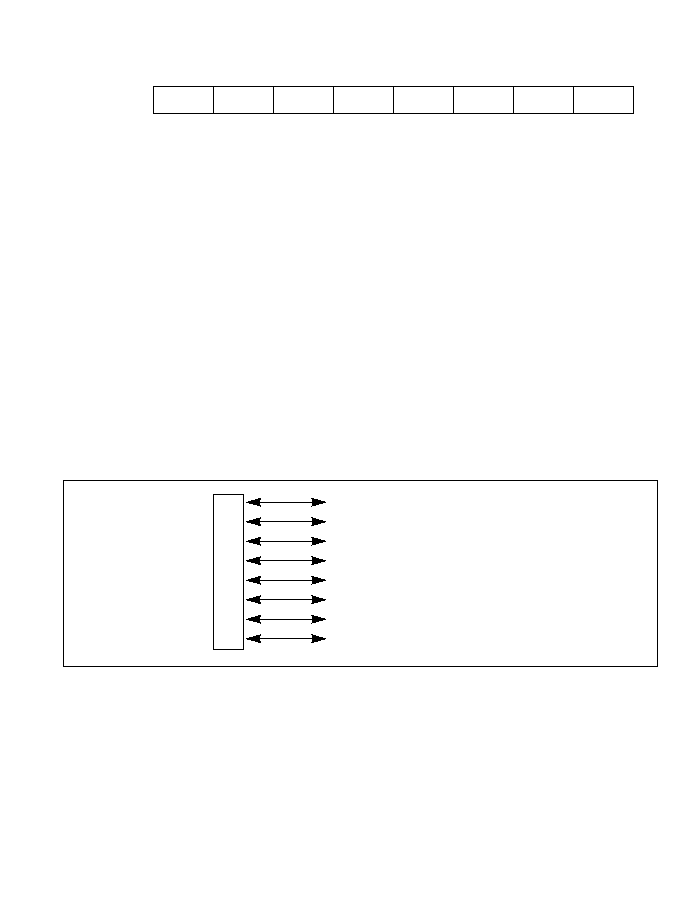
2. Port 3 Data Register (P3DR)--H'FF86
P3DR is an 8-bit register containing the data for pins P3
7
to P3
0
.
At a reset and in the hardware standby mode, P3DR is initialized to H'00.
When the CPU reads P3DR, for output pins it reads the value in the P3DR latch, but for input
pins, it obtains the pin status directly.
9.4.3 Pin Functions in Each Mode
Port 3 has different functions in the expanded modes (modes 1, 2, 3, 4) and the single-chip mode
(mode 7). Separate descriptions are given below.
Pin Functions in Expanded Modes: In the expanded modes (modes 1, 2, 3, and 4), port 3 is
automatically used as the data bus and P3DDR is ignored. Figure 9-6 shows the pin functions
for the expanded modes.
Bit
7
6
5
4
3
2
1
0
P3
7
P3
6
P3
5
P3
4
P3
3
P3
2
P3
1
P3
0
Initial value
0
0
0
0
0
0
0
0
Read/Write
R/W
R/W
R/W
R/W
R/W
R/W
R/W
R/W
D
7
(input/output)
D
6
(input/output)
D
5
(input/output)
Port
D
4
(input/output)
3
D
3
(input/output)
D
2
(input/output)
D
1
(input/output)
D
0
(input/output)
Figure 9-6 Port 3 Pin Functions in Expanded Modes
153

Pin Functions in Single-Chip Mode: In the single-chip mode (mode 7), each of the port 3 pins
can be designated as an input pin or an output pin, as indicated in figure 9-7, by setting the
corresponding bit in P3DDR to "1" for output or clearing it to "0" for input.
9.5 Port 4
9.5.1 Overview
Port 4 is an 8-bit input/output port with the pin configuration shown in figure 9-8. In the
expanded modes it provides the low bits (A
7
≠ A
0
) of the address bus. In the single-chip mode it
operates as a general-purpose input/output port.
Outputs from port 4 can drive one TTL load and a 90pF capacitive load. They can also drive a
Darlington transistor pair or LED (with 8mA current sink).
P3
7
(input/output)
P3
6
(input/output)
P3
5
(input/output)
Port
P3
4
(input/output)
3
P3
3
(input/output)
P3
2
(input/output)
P3
1
(input/output)
P3
0
(input/output)
Pin
Expanded Modes
Single-Chip Mode
P4
7
/ A
7
A
7
(output)
P4
7
(input/output)
P4
6
/ A
6
A
6
(output)
P4
6
(input/output)
P4
5
/ A
5
A
5
(output)
P4
5
(input/output)
Port
P4
4
/ A
4
A
4
(output)
P4
4
(input/output)
4
P4
3
/ A
3
A
3
(output)
P4
3
(input/output)
P4
2
/ A
2
A
2
(output)
P4
2
(input/output)
P4
1
/ A
1
A
1
(output)
P4
1
(input/output)
P4
0
/ A
0
A
0
(output)
P4
0
(input/output)
Figure 9-7 Port 3 Pin Functions in Single-Chip Mode
Figure 9-8 Pin Functions of Port 4
154

9.5.2 Port 4 Registers
Register Configuration: Table 9-7 lists the registers of port 4.
Table 9-7 Port 4 Registers
Name
Abbreviation
Read/Write
Initial Value
Address
Port 4 data direction register
P4DDR
W
H'00
H'FF85
Port 4 data register
P4DR
R/W
H'00
H'FF87
1. Port 4 Data Direction Register (P4DDR)--H'FF85
P4DDR is an 8-bit register that selects the direction of each pin in port 4.
Single-Chip Mode: A pin functions as an output pin if the corresponding bit in P4DDR is set
to "1," and as in input pin if the bit is cleared to "0."
P4DDR can be written but not read. An attempt to read this register does not cause an error, but
all bits are read as "1," regardless of their true values.
At a reset and in the hardware standby mode, P4DDR is initialized to H'00, making all eight pins
input pins. P4DDR is not initialized in the software standby mode, so if a P4DDR bit is set to "1"
when the chip enters the software standby mode, the corresponding pin continues to output the
value in the port 4 data register.
Expanded Modes: All bits of P4DDR are fixed at "1" and cannot be modified.
Bit
7
6
5
4
3
2
1
0
P4
7
DDR P4
6
DDR P4
5
DDR P4
4
DDR P4
3
DDR P4
2
DDR P4
1
DDR P4
0
DDR
Initial value
0
0
0
0
0
0
0
0
Read/Write
W
W
W
W
W
W
W
W
155

2. Port 4 Data Register (P4DR)--H'FF87
P4DR is an 8-bit register containing the data for pins P4
7
to P4
0
.
At a reset and in the hardware standby mode, P4DR is initialized to H'00.
When the CPU reads P4DR, for output pins it reads the value in the P4DR latch, but for input
pins, it obtains the pin status directly.
9.5.3 Pin Functions in Each Mode
Port 4 has different functions in the expanded modes (modes 1, 2, 3, 4) and the single-chip mode
(mode 7). Separate descriptions are given below.
Pin Functions in Expanded Modes: In the expanded modes (modes 1, 2, 3, and 4), port 4 is
used for output of the low bits (A
7
≠ A
0
) of the address bus. P4DDR is automatically set for
output. Figure 9-9 shows the pin functions for the expanded modes.
Pin Functions in Single-Chip Mode: In the single-chip mode (mode 7), each of the port 4
pins can be designated as an input pin or an output pin, as indicated in figure 9-10, by setting
the corresponding bit in P4DDR to "1" for output or clearing it to "0" for input.
Bit
7
6
5
4
3
2
1
0
P4
7
P4
6
P4
5
P4
4
P4
3
P4
2
P4
1
P4
0
Initial value
0
0
0
0
0
0
0
0
Read/Write
R/W
R/W
R/W
R/W
R/W
R/W
R/W
R/W
A
7
(output)
A
6
(output)
A
5
(output)
Port
A
4
(output)
4
A
3
(output)
A
2
(output)
A
1
(output)
A
0
(output)
Figure 9-9 Port 4 Pin Functions in Expanded Modes
156
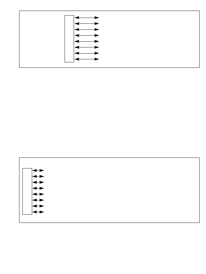
9.6 Port 5
9.6.1 Overview
Port 5 is an 8-bit input/output port with the pin configuration shown in figure 9-11. In the
expanded modes that use the on-chip ROM (modes 2 and 4), the pins of port 5 function either as
general-purpose input pins or as bits A
15
≠ A
8
of the address bus, depending on the port 5 data
direction register (P5DDR).
Port 5 has built-in MOS pull-ups that can be turned on or off under program control.
Outputs from port 5 can drive one TTL load and a 90pF capacitive load. They can also drive a
Darlington transistor pair.
P4
7
(input/output)
P4
6
(input/output)
P4
5
(input/output)
Port
P4
4
(input/output)
4
P4
3
(input/output)
P4
2
(input/output)
P4
1
(input/output)
P4
0
(input/output)
Pin
Modes 1 and 3
Modes 2 and 4
Single-Chip Mode
P5
7
/ A
15
A
15
(output)
P5
7
(input) / A
15
(output)
P5
7
(input/output)
P5
6
/ A
14
A
14
(output)
P5
6
(input) / A
14
(output)
P5
6
(input/output)
P5
5
/ A
13
A
13
(output)
P5
5
(input) / A
13
(output)
P5
5
(input/output)
Port
P5
4
/ A
12
A
12
(output)
P5
4
(input) / A
12
(output)
P5
4
(input/output)
5
P5
3
/ A
11
A
11
(output)
P5
3
(input) / A
11
(output)
P5
3
(input/output)
P5
2
/ A
10
A
10
(output)
P5
2
(input) / A
10
(output)
P5
2
(input/output)
P5
1
/ A
9
A
9
(output)
P5
1
(input) / A
9
(output)
P5
1
(input/output)
P5
0
/ A
8
A
8
(output)
P5
0
(input) / A
8
(output)
P5
0
(input/output)
Figure 9-10 Port 4 Pin Functions in Single-Chip Mode
Figure 9-11 Pin Functions of Port 5
157

9.6.2 Port 5 Registers
Register Configuration: Table 9-8 lists the registers of port 5.
Table 9-8 Port 5 Registers
Name
Abbreviation
Read/Write
Initial Value
Address
Port 5 data direction register
P5DDR
W
H'00
H'FF88
Port 5 data register
P5DR
R/W
H'00
H'FF8A
1. Port 5 Data Direction Register (P5DDR)--H'FF88
P5DDR is an 8-bit register that selects the direction of each pin in port 5.
Single-Chip Mode: A pin functions as an output pin if the corresponding bit in P5DDR is set
to "1," and as an input pin if the bit is cleared to "0."
P5DDR can be written but not read. An attempt to read this register does not cause an error,
but all bits are read as "1," regardless of their true values.
At a reset and in the hardware standby mode, P5DDR is initialized to H'00, making all eight
pins input pins. P5DDR is not initialized in the software standby mode, so if a P5DDR bit is
set to "1" when the chip enters the software standby mode, the corresponding pin continues to
output the value in the port 5 data register.
Expanded Modes Using On-Chip ROM (Modes 2 and 4): If a "1" is set in P5DDR, the
corresponding pin is used for address output. If a "0" is set in P5DDR, the pin is used for
general-purpose input. P5DDR is initialized to H'00 at a reset and in the hardware standby
mode.
Expanded Modes Not Using On-Chip ROM (Modes 1 and 3): All bits of P5DDR are fixed
at "1" and cannot be modified.
Bit
7
6
5
4
3
2
1
0
P5
7
DDR P5
6
DDR P5
5
DDR P5
4
DDR P5
3
DDR P5
2
DDR P5
1
DDR P5
0
DDR
Initial value
0
0
0
0
0
0
0
0
Read/Write
W
W
W
W
W
W
W
W
158

Port 5 Data Register (P5DR)--H'FF8A
P5DR is an 8-bit register containing the data for pins P5
7
to P5
0
.
At a reset and in the hardware standby mode, P5DR is initialized to H'00.
When the CPU reads P5DR, for output pins it reads the value in the P5DR latch, but for input
pins, it obtains the pin status directly.
9.6.3 Pin Functions in Each Mode
Port 5 operates in one way in modes 1 and 3, in another way in modes 2 and 4, and in a third way
in mode 7. Separate descriptions are given below.
Pin Functions in Modes 1 and 3: In modes 1 and 3 (expanded modes in which the on-chip ROM
is not used), all bits of P5DDR are automatically set to "1" for output, and the pins of port 5 carry
bits A
15
≠ A
8
of the address bus. Figure 9-12 shows the pin functions for modes 1 and 3.
Bit
7
6
5
4
3
2
1
0
P5
7
P5
6
P5
5
P5
4
P5
3
P5
2
P5
1
P5
0
Initial value
0
0
0
0
0
0
0
0
Read/Write
R/W
R/W
R/W
R/W
R/W
R/W
R/W
R/W
A
15
(output)
A
14
(output)
A
13
(output)
Port
A
12
(output)
5
A
11
(output)
A
10
(output)
A
9
(output)
A
8
(output)
Figure 9-12 Port 5 Pin Functions in Modes 1 and 3
159
Pin Functions in Modes 2 and 4: In modes 2 and 4, (expanded modes in which the on-chip
ROM is used), software can select whether to use port 5 for general-purpose input, or for
output of bits A
15
≠ A
8
of the address bus.
If a bit in P5DDR is set to "1," the corresponding pin is used for address output. If the bit is
cleared to "0," the pin is used for input. A reset clears all P5DDR bits to "0," so before the
address bus is used, all necessary bits in P5DDR must be set to "1."
Figure 9-13 shows the pin functions in modes 2 and 4.
Pin Functions in Single-Chip Mode: In the single-chip mode (mode 7), each of the port 5
pins can be designated as an input pin or an output pin, as indicated in figure 9-14, by setting
the corresponding bit in P5DDR to "1" for output or clearing it to "0" for input.
When P5DDR
When P5DDR Bit
Bit is Set to "1"
is Cleared to "0"
A
15
(output)
P5
7
(input)
A
14
(output)
P5
6
(input)
A
13
(output)
P5
5
(input)
Port
A
12
(output)
P5
4
(input)
5
A
11
(output)
P5
3
(input)
A
10
(output)
P5
2
(input)
A
9
(output)
P5
1
(input)
A
8
(output)
P5
0
(input)
P5
7
(input/output)
P5
6
(input/output)
P5
5
(input/output)
Port
P5
4
(input/output)
5
P5
3
(input/output)
P5
2
(input/output)
P5
1
(input/output)
P5
0
(input/output)
Figure 9-13 Port 5 Pin Functions in Modes 2 and 4
Figure 9-14 Port 5 Pin Functions in Single-Chip Mode
160

9.6.4 Built-In MOS Pull-Up
The MOS input pull-ups of port 5 are turned on by clearing the corresponding bit in P5DDR to
"0" and writing a "1" in P5DR. These pull-ups are turned off at a reset and in the hardware
standby mode. Table 9-9 indicates the status of the MOS pull-ups in various modes.
Table 9-9 Status of MOS Pull-Ups for Port 5
Mode
Reset
Hardware Standby Mode
Other Operating States
*
1
OFF
OFF
OFF
2
ON/OFF
3
OFF
4
7
*
Including the software standby mode.
Notation:
OFF:
The MOS pull-up is always off.
ON/OFF:
The MOS pull-up is on when P5DDR = 0 and P5DR = 1, and off otherwise.
Note on Usage of MOS Pull-Ups
If the bit manipulation instructions listed below are executed on input/output ports 5 and 6 which
have selectable MOS pull-ups, the logic levels at input pins will be transferred to the DR latches,
causing the MOS pull-ups to be unintentionally switched on or off.
This can occur with the following bit manipulation instructions: BSET, BCLR, BNOT
(1)
Specific Example (BSET Instruction): An example will be shown in which the BSET
instruction is executed for port 5 under the following conditions:
P5
7
:
Input pin, low, MOS pull-up transistor on
P5
6
:
Input pin, high, MOS pull-up transistor off
P5
5
≠ P5
0
: Output pins, low
The intended purpose of this BSET instruction is to switch the output level at P5
0
from low
to high.
ON/OFF
161

162
A: Before Execution of BSET Instruction
P5
7
P5
6
P5
5
P5
4
P5
3
P5
2
P5
1
P5
0
Input/output
Input
Input
Output
Output
Output
Output
Output
Output
Pin state
Low
High
Low
Low
Low
Low
Low
Low
DDR
0
0
1
1
1
1
1
1
DR
1
0
0
0
0
0
0
0
Pull-up
On
Off
Off
Off
Off
Off
Off
Off
B: Execution of BSET Instruction
BSET.B #0
@PORT5
;set bit 0 in data register
C: After Execution of BSET Instruction
P5
7
P5
6
P5
5
P5
4
P5
3
P5
2
P5
1
P5
0
Input/output
Input
Input
Output
Output
Output
Output
Output
Output
Pin state
Low
High
Low
Low
Low
Low
Low
High
DDR
0
0
1
1
1
1
1
1
DR
0
1
0
0
0
0
0
1
Pull-up
Off
On
Off
Off
Off
Off
Off
Off
Explanation: To execute the BSET instruction, the CPU begins by reading port 5. Since P5
7
and
P5
6
are input pins, the CPU reads the level of these pins directly, not the value in the data register.
It reads P5
7
as low (0) and P5
6
as high (1).
Since P5
5
to P5
0
are output pins, for these pins the CPU reads the value in the data register (0).
The CPU therefore reads the value of port 5 as H'40, although the actual value in P5DR is H'80.
Next the CPU sets bit 0 of the read data to 1, changing the value to H'41.
Finally, the CPU writes this value (H'41) back to P5DR to complete the BSET instruction.
As a result, bit P5
0
is set to 1, switching pin P5
0
to high output. In addition, bits P5
7
and P5
6
are
both modified, changing the on/off settings of the MOS pull-up transistors of pins P5
7
and P5
6
.
Programming Solution: The switching of the pull-ups for P5
7
and P5
6
in the preceding example
can be avoided by using a byte in RAM as a work area for P5DR, performing bit manipulations on
the work area, then writing the result to P5DR.

A: Before Execution of BSET Instruction
MOV.B #80, R0
;write data (H'80) for data register
MOV.B R0, @RAM0
;write to work area (RAM0)
MOV.B R0, @PORT5
;write to P5DR
P5
7
P5
6
P5
5
P5
4
P5
3
P5
2
P5
1
P5
0
Input/output
Input
Input
Output
Output
Output
Output
Output
Output
Pin state
Low
High
Low
Low
Low
Low
Low
Low
DDR
0
0
1
1
1
1
1
1
DR
1
0
0
0
0
0
0
0
Pull-up
On
Off
Off
Off
Off
Off
Off
Off
RAM0
1
0
0
0
0
0
0
0
B: Execution of BSET Instruction
BSET.B #0, @RAM0
;set bit 0 in work area (RAM0)
C: After Execution of BSET Instruction
MOV.B @RAM0, R0
;get value in work area (RAM0)
MOV.B R0, @PORT5
;write value to P5DR
P5
7
P5
6
P5
5
P5
4
P5
3
P5
2
P5
1
P5
0
Input/output
Input
Input
Output
Output
Output
Output
Output
Output
Pin state
Low
High
Low
Low
Low
Low
Low
High
DDR
0
0
1
1
1
1
1
1
DR
1
0
0
0
0
0
0
1
Pull-up
On
Off
Off
Off
Off
Off
Off
Off
RAM0
1
0
0
0
0
0
0
0
9.7 Port 6
9.7.1 Overview
Port 6 is a 4-bit input/output port with the pin configuration shown in figure 9-15. In mode 4 (the
expanded maximum mode that uses the on-chip ROM), the pins of port 6 function either as
general-purpose input pins or as the page address bus, depending on the port 6 data direction
register (P6DDR).
Port 6 has built-in MOS pull-ups that can be turned on or off under program control.
Outputs from port 6 can drive one TTL load and a 90pF capacitive load. They can also drive a
Darlington transistor pair.
163
9.7.2 Port 6 Registers
Register Configuration: Table 9-10 lists the registers of port 6.
Table 9-10 Port 6 Registers
Name
Abbreviation
Read/Write
Initial Value
Address
Port 6 data direction register
P6DDR
W
H'F0
H'FF89
Port 6 data register
P6DR
R/W
H'F0
H'FF8B
1. Port 6 Data Direction Register (P6DDR)--H'FF89
P6DDR is an 8-bit register that selects the direction of each pin in port 6.
Single-Chip Mode and Expanded Minimum Modes: A pin functions as an output pin if the
corresponding bit in P6DDR is set to "1," and as an input pin if the bit is cleared to "0."
Bits 3 to 0 can be written but not read. An attempt to read these bits does not cause an error, but
all bits are read as "1," regardless of their true values.
Pin
Mode 3
Mode 4
Mode 1 and 2 and
Single-Chip Mode
P6
3
/ A
19
A
19
(output)
P6
3
(input) / A
19
(output)
P6
3
(input/output)
Port
P6
2
/ A
18
A
18
(output)
P6
2
(input) / A
18
(output)
P6
2
(input/output)
6
P6
1
/ A
17
A
17
(output)
P6
1
(input) / A
17
(output)
P6
1
(input/output)
P6
0
/ A
16
A
16
(output)
P6
0
(input) / A
16
(output)
P6
0
(input/output)
Bit
7
6
5
4
3
2
1
0
--
--
--
--
P6
3
DDR P6
2
DDR P6
1
DDR P6
0
DDR
Initial value
1
1
1
1
0
0
0
0
Read/Write
--
--
--
--
W
W
W
W
Figure 9-15 Pin Functions of Port 6
164

Bits 7 to 4 are reserved. They cannot be modified and are always read as "1."
At a reset and in the hardware standby mode, P6DDR is initialized to H'F0, making all four pins
input pins. P6DDR is not initialized in the software standby mode, so in the single-chip mode, or
expanded minimum mode, if a P6DDR bit is set to "1" when the chip enters the software standby
mode, the corresponding pin continues to output the value in the port 6 data register.
Expanded Maximum Mode Using On-Chip ROM (Mode 4): If a "1" is set in P6DDR, the
corresponding pin is used for address output. If a "0" is set in P6DDR, the pin is used for
input. P6DDR is initialized to H'F0 at a reset and in the hardware standby mode.
Expanded Maximum Mode Not Using On-Chip ROM (Mode 3): All bits of P6DDR are
fixed at "1" and cannot be modified.
2. Port 6 Data Register (P6DR)--H'FF8B
P6DR is an 8-bit register containing the data for pins P6
3
to P6
0
.
Bits 7 to 4 are reserved. They cannot be modified and are always read as "1."
At a reset and in the hardware standby mode, P6DR is initialized to H'F0.
When the CPU reads P6DR, for output pins it reads the value in the P6DR latch, but for input
pins, it obtains the pin status directly.
9.7.3 Pin Functions in Each Mode
The usage of port 6 depends on the MCU operating mode. Separate descriptions are given below.
Pin Functions in Mode 3: In mode 3 (the expanded maximum mode in which the on-chip ROM
is not used), P6DDR is automatically set for output, and the pins of port 6 carry the page address
bits (A
19
≠ A
16
) of the address bus. Figure 9-16 shows the pin functions for mode 3.
Bit
7
6
5
4
3
2
1
0
--
--
--
--
P6
3
P6
2
P6
1
P6
0
Initial value
1
1
1
1
0
0
0
0
Read/Write
--
--
--
--
R/W
R/W
R/W
R/W
165
Pin Functions in Mode 4: In mode 4, (the expanded maximum mode in which the on-chip ROM
is used), software can select whether to use port 6 for general-purpose input, or for output of the
page address bits.
If a bit in P6DDR is set to "1," the corresponding pin is used for page address output. If the bit is
cleared to "0," the pin is used for input. A reset initializes these pins to the general-purpose input
function, so when the address bus is used, all necessary bits in P6DDR must first be set to "1."
Figure 9-17 shows the pin functions in mode 4.
Pin Functions in Single-Chip Mode and Expanded Minimum Modes: In the single-chip mode
(mode 7) and expanded minimum modes (modes 1 and 2), each of the port 6 pins can be
designated as an input pin or an output pin, as indicated in figure 9-18, by setting the
corresponding bit in P6DDR to "1" for output or clearing it to "0" for input.
A
19
(output)
Port
A
18
(output)
6
A
17
(output)
A
16
(output)
When P6DDR Bit
When P6DDR Bit
Is Set to "1"
is Cleared to "0"
A
19
(output)
P6
3
(input)
Port
A
18
(output)
P6
2
(input)
6
A
17
(output)
P6
1
(input)
A
16
(output)
P6
0
(input)
Figure 9-16 Port 6 Pin Functions in Mode 3
Figure 9-17 Port 6 Pin Functions in Mode 4
166

9.7.4 Built-in MOS Pull-Up
Port 6 has programmable MOS input pull-ups which are turned on by clearing the corresponding
bit in P6DDR to "0" and writing a "1" in P6DR. These pull-ups are turned off at a reset and in the
hardware standby mode. Table 9-11 indicates the status of the MOS pull-ups in various modes.
Table 9-11 Status of MOS Pull-Ups for Port 5
Mode
Reset
Hardware Standby Mode
Other Operating States
*
1
OFF
OFF
2
3
OFF
4
7
*
Including the software standby mode.
Notation:
OFF:
The MOS pull-up is always off.
ON/OFF:
The MOS pull-up is on when P6DDR = 0 and P6DR = 1, and off otherwise.
Note: When using the built-in pull-ups, see the "Note on Usage of MOS Pull-Ups" in
section 9.6.4.
9.8 Port 7
9.8.1 Overview
Port 7 is an 8-bit input/output port with the pin configuration shown in figure 9-19. Its pins also
carry input and output signals for the on-chip free-running timers (FRT1, FRT2, and FRT3), and
two input signals for the on-chip 8-bit timer.
P6
3
(input/output)
Port
P6
2
(input/output)
6
P6
1
(input/output)
P6
0
(input/output)
ON/OFF
ON/OFF
Figure 9-18 Port 6 Pin Functions in Modes 7, 2, and 1
167
Port 7 has Schmitt inputs. Outputs from port 7 can drive one TTL load and a 30pF capacitive
load. They can also drive a Darlington transistor pair.
9.8.2 Port 7 Registers
Register Configuration: Table 9-12 lists the registers of port 7.
Table 9-12 Port 7 Registers
Name
Abbreviation
Read/Write
Initial Value
Address
Port 7 data direction register
P7DDR
W
H'00
H'FF8C
Port 7 data register
P7DR
R/W
H'00
H'FF8E
1. Port 7 Data Direction Register (P7DDR)--H'FF8C
P7DDR is an 8-bit register that selects the direction of each pin in port 7. A pin functions as an
output pin if the corresponding bit in P7DDR is set to "1," and as an input pin if the bit is cleared
to "0."
P7DDR can be written but not read. An attempt to read this register does not cause an error, but
all bits are read as "1," regardless of their true values.
At a reset and in the hardware standby mode, P7DDR is initialized to H'00, setting all pins for
input. P7DDR is not initialized in the software standby mode, so if a P7DDR bit is set to "1"
when the chip enters the software standby mode, the corresponding pin continues to output the
value in the port 7 data register.
P7
7
(input/output) / FTOA
1
(output)
P7
6
(input/output) / FTOB
3
(output) / FTCI
3
(input)
P7
5
(input/output) / FTOB
2
(output) / FTCI
2
(input)
Port
P7
4
(input/output) / FTOB
1
(output) / FTCI
1
(input)
7
P7
3
(input/output) / FTI
3
(input) /TMRI (input)
P7
2
(input/output) / FTI
2
(input)
P7
1
(input/output) / FTI
1
(input)
P7
0
(input/output) / TMCI (input)
Bit
7
6
5
4
3
2
1
0
P7
7
DDR P7
6
DDR P7
5
DDR P7
4
DDR P7
3
DDR P7
2
DDR P7
1
DDR P7
0
DDR
Initial value
0
0
0
0
0
0
0
0
Read/Write
W
W
W
W
W
W
W
W
Figure 9-19 Pin Functions of Port 7
168

A transition to the software standby mode initializes the on-chip supporting modules, so any pins
of port 7 that were being used by an on-chip timer when the transition occurs revert to general-
purpose input or output, controlled by P7DDR and P7DR.
2. Port 7 Data Register (P7DR)--H'FF8E
P7DR is an 8-bit register containing the data for pins P7
7
to P7
0
. When the CPU reads P7DR, for
output pins it reads the value in the P7DR latch, but for input pins, it obtains the pin status directly.
9.8.3 Pin Functions
The pin functions of port 7 are the same in all MCU operating modes. As figure 9-19 indicated,
these pins are used for input and output of on-chip timer signals as well as for general-purpose
input and output. For some pins, two or more functions can be enabled simultaneously.
P7
7
can be used either for general-purpose input/output, or as the output pin for the output
compare A signal (FTOA) from free-running timer 1.
P7
6
to P7
4
can be used either for general-purpose input/output, or as the output pins for the output
compare B signals (FTOB) from free-running timers 3 to 1. When used for general-purpose input
and output, they can also provide external clock input (FTCI) to the free-running counters. This
additional function is selected when the clock select 1 and 0 bits (CKS1 and CKS0) in the free-
running timer control registers are both set to "1."
P7
3
to P7
1
function simultaneously as general-purpose input/output pins and as input pins for the
input capture signals (FTI) of free-running timers 3 to 1.
Bit
7
6
5
4
3
2
1
0
P7
7
P7
6
P7
5
P7
4
P7
3
P7
2
P7
1
P7
0
Initial value
0
0
0
0
0
0
0
0
Read/Write
R/W
R/W
R/W
R/W
R/W
R/W
R/W
R/W
169
P7
3
and P7
0
can be used for timer reset input (TMRI) and timer clock input (TMCI) for the 8-bit
timer, as well as for general-purpose input and output.
Table 9-13 shows how the functions of the pins of port 7 are selected.
Table 9-13 Port 7 Pin Functions
Pin
Selection of Pin Functions
P7
7
/
The function depends on the output enable A bit (OEA) of the FRT1 timer control
FTOA
1
register (TCR) and on the P7
7
DDR bit as follows:
OEA
0
1
P7
7
DDR
0
1
0
1
Pin function
P7
7
input
P7
7
output
FTOA
1
output
P7
6
/
The function depends on the output compare B bit (OEB) of the FRT3 timer control
FTOB
3
/
register (TCR) and on the P7
6
DDR bit as follows:
FTCI
3
OEB
0
1
P7
6
DDR
0
1
0
1
Pin function
P7
6
input
P7
6
output
FTOB
3
output
FTCI
3
input
P7
5
/
The function depends on the output compare B bit (OEB) of the FRT2 timer control
FTOB
2
/
register (TCR) and on the P7
5
DDR bit as follows:
FTCI
2
OEB
0
1
P7
5
DDR
0
1
0
1
Pin function
P7
5
input
P7
5
output
FTOB
2
output
FTCI
2
input
P7
4
/
The function depends on the output compare B bit (OEB) of the FRT1 timer control
FTOB
1
/
register (TCR) and on the P7
4
DDR bit as follows:
FTCI
1
OEB
0
1
P7
4
DDR
0
1
0
1
Pin function
P7
4
input
P7
4
output
FTOB
1
output
FTCI
1
input
170

Table 9-13 Port 7 Pin Functions (cont)
Pin
Selection of Pin Functions
P7
3
/ FTI
3
/
The function depends on the counter clear bits 1 and 0 (CCLR1 and CCLR0) in the
TMRI
timer control register (TCR) of the 8-bit timer, and on the P7
3
DDR bit as follows:
CCLR1, CCLR0: At least one bit is "0." Both bits are set to "1"
P7
3
DDR
0
1
Pin function
P7
3
input
P7
3
output
FTI
3
input and TMRI input
P7
2
/ FTI
2
P7
2
DDR
0
1
Pin function
P7
2
input
P7
2
output
FTI
2
input
P7
1
/ FTI
1
P7
1
DDR
0
1
Pin function
P7
1
input
P7
1
output
FTI
1
input
P7
0
/ TMCI
This pin always has a general-purpose input/output function, and can simultaneously
be used for external clock input for the 8-bit timer, depending on clock select bits 2 to
0 (CKS2, CKS1, and CKS0) in the timer control register (TCR). See section 11, "8-
bit Timer" for details.
P7
0
DDR
0
1
Pin function
P7
0
input
P7
0
output
TMCI input
171
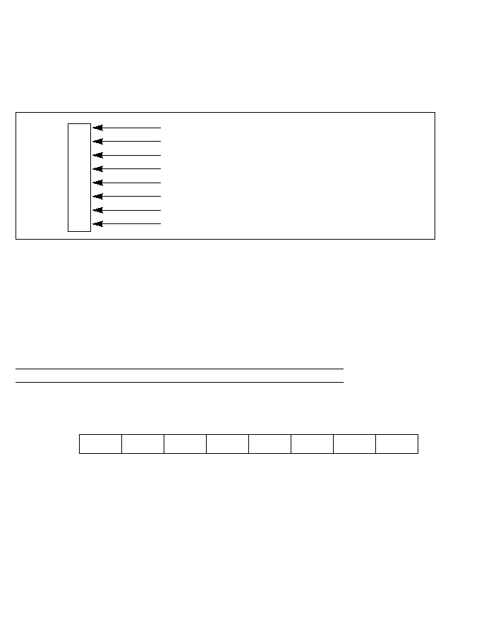
9.9 Port 8
9.9.1 Overview
Port 8 is an 8-bit input port that also receives inputs for the on-chip A/D converter. The pin
functions are the same in all MCU operating modes, as shown in figure 9-20.
9.9.2 Port 8 Registers
Register Configuration: Port 8 has only the data register described in table 9-14. Since it is
exclusively an input port, there is no data direction register.
Table 9-14 Port 8 Registers
Name
Abbreviation
Read/Write
Address
Port 8 data register
P8DR
R
H'FF8F
1. Port 8 Data Register (P8DR)--H'FF8F
When the CPU reads P8DR it always reads the current status of each pin, except that during A/D
conversion the pin currently being converted reads "1" regardless of the actual input voltage at that
pin.
P8
7
(input) / AN
7
(input)
P8
6
(input) / AN
6
(input)
P8
5
(input) / AN
5
(input)
Port
P8
4
(input) / AN
4
(input)
8
P8
3
(input) / AN
3
(input)
P8
2
(input) / AN
2
(input)
P8
1
(input) / AN
1
(input)
P8
0
(input) / AN
0
(input)
Bit
7
6
5
4
3
2
1
0
P8
7
P8
6
P8
5
P8
4
P8
3
P8
2
P8
1
P8
0
Initial value
0
0
0
0
0
0
0
0
Read/Write
R
R
R
R
R
R
R
R
Figure 9-20 Pin Functions of Port 8
172
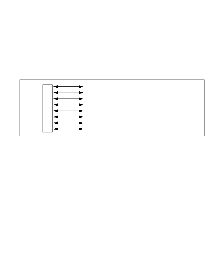
9.10 Port 9
9.10.1 Overview
Port 9 is an 8-bit input/output port with the pin configuration shown in figure 9-21. In addition to
general-purpose input and output, its pins are used for the output compare A signals from free-
running timers 2 and 3, for PWM timer output, and for input and output by the on-chip serial
communication interface 9 (SCI). The pin functions are the same in all MCU operating modes.
Outputs from port 9 can drive one TTL load and a 30pF capacitive load. They can also drive a
Darlington transistor pair.
Figure 9-21 Pin Functions of Port 9
9.10.2 Port 9 Registers
Register Configuration: Table 9-15 lists the registers of port 9.
Table 9-15 Port 9 Registers
Name
Abbreviation
Read/Write
Initial Value
Address
Port 9 data direction register
P9DDR
W
H'00
H'FFFE
Port 9 data register
P9DR
R/W
H'00
H'FFFF
P9
7
(input/output) / SCK (input/output)
P9
6
(input/output) / RXD (input)
P9
5
(input/output) / TXD (output)
Port
P9
4
(input/output) / PW
3
(output)
9
P9
3
(input/output) / PW
2
(output)
P9
2
(input/output) / PW
1
(output)
P9
1
(input/output) / FTOA
3
(output)
P9
0
(input/output) / FTOA
2
(output)
173

1. Port 9 Data Direction Register (P9DDR)--H'FFFE
P9DDR is an 8-bit register that selects the direction of each pin in port 9. A pin functions as an
output pin if the corresponding bit in P9DDR is set to "1," and as an input pin if the bit is cleared
to "0."
P9DDR can be written but not read. An attempt to read this register does not cause an error, but
all bits are read as "1," regardless of their true values.
At a reset and in the hardware standby mode, P9DDR is initialized to H'00, setting all pins for
input. P9DDR is not initialized in the software standby mode, so if a P9DDR bit is set to "1"
when the chip enters the software standby mode, the corresponding pin continues to output the
value in the port 9 data register.
A transition to the software standby mode initializes the on-chip supporting modules, so any pins
of port 9 that were being used by an on-chip module (example: free-running timer output) when
the transition occurs revert to general-purpose input or output, controlled by P9DDR and P9DR.
2. Port 9 Data Register (P9DR)--H'FFFF
P9DR is an 8-bit register containing the data for pins P9
7
to P9
0
. When the CPU reads P9DR, for
output pins it reads the value in the P9DR latch, but for input pins, it obtains the pin status directly.
9.10.3 Pin Functions
The pin functions of port 9 are the same in all MCU operating modes. As figure 9-21 indicated,
these pins are used for output of on-chip timer signals and for input and output of serial data and
clock signals as well as for general-purpose input and output. Specifically, they carry output
signals for free-running timers 2 and 3, output signals for the pulse-width modulation (PWM)
timer, and input and output signals for the serial communication interface.
Bit
7
6
5
4
3
2
1
0
P9
7
DDR P9
6
DDR P9
5
DDR P9
4
DDR P9
3
DDR P9
2
DDR P9
1
DDR P9
0
DDR
Initial value
0
0
0
0
0
0
0
0
Read/Write
W
W
W
W
W
W
W
W
Bit
7
6
5
4
3
2
1
0
P9
7
P9
6
P9
5
P9
4
P9
3
P9
2
P9
1
P9
0
Initial value
0
0
0
0
0
0
0
0
Read/Write
R/W
R/W
R/W
R/W
R/W
R/W
R/W
R/W
174

Table 9-16 shows how the functions of the pins of port 9 are selected.
Table 9-16 Port 9 Pin Functions
Pin
Selection of Pin Functions
P9
7
/
The function depends on the communication mode bit (C/A) and the clock enable 1
SCK
and 2 bits (CKE1 and CKE0) of the serial control register (SCR) of the serial
communication interface as follows:
C/A
0
1
CKE1
0
1
0
1
CKE0
0
1
0
1
0
1
0
1
Pin function P9
7
SCI
SCI external
SCI internal
SCI external
input
internal clock input
clock output
clock input
or
clock
output
*
output
*
Input or output is selected by the P9
7
DDR bit.
P9
6
/ RXD
The function depends on the receive enable bit (RE) of the serial control register
(SCR) and on the P9
6
DDR bit as follows:
RE
0
1
P9
6
DDR
0
1
0
1
Pin function
P9
6
input
P9
6
output
RXD input
P9
5
/ TXD
The function depends on the transmit enable bit (TE) of the serial control register
(SCR) and on the P9
5
DDR bit as follows:
TE
0
1
P9
5
DDR
0
1
0
1
Pin function
P9
5
input
P9
5
output
TXD output
175

Table 9-16 Port 9 Pin Functions (cont)
Pin
Selection of Pin Functions
P9
4
/ PW
3
The function depends on the output enable bit (OE) of the timer control register of
PWM timer channel 3 and on the P9
4
DDR bit as follows:
OE
0
1
P9
4
DDR
0
1
0
1
Pin function
P9
4
input
P9
4
output
PW
3
output
P9
3
/ PW
2
The function depends on the output enable bit (OE) of the timer control register of
PWM timer channel 2 and on the P9
3
DDR bit as follows:
OE
0
1
P9
3
DDR
0
1
0
1
Pin function
P9
3
input
P9
3
output
PW
2
output
P9
2
/ PW
1
The function depends on the output enable bit (OE) of the timer control register of
PWM timer channel 1 and on the P9
2
DDR bit as follows:
OE
0
1
P9
2
DDR
0
1
0
1
Pin function
P9
2
input
P9
2
output
PW
1
output
P9
1
/
The function depends on the output compare A bit (OEA) of the FRT3 timer control
FTOA
3
FTOA
3
register (TCR) and on the P9
1
DDR bit as follows:
OEA
0
1
P9
1
DDR
0
1
0
1
Pin function
P9
1
input
P9
1
output
FTOA
3
output
P9
0
/
The function depends on the output compare A bit (OEA) of the FRT3 timer control
FTOA
2
FTOA
2
register (TCR) and on the P9
0
DDR bit as follows:
OEA
0
1
P9
0
DDR
0
1
0
1
Pin function
P9
0
input
P9
0
output
FTOA
2
output
176

Section 10 16-Bit Free-Running Timers
10.1 Overview
The H8/532 has an on-chip 16-bit free-running timer (FRT) module with three independent
channels (FRT1, FRT2, and FRT3). All three channels are functionally identical.
Each channel has a 16-bit free-running counter that it uses as a time base. Applications of the
FRT module include rectangular-wave output (up to two independent waveforms per channel),
input pulse width measurement, and measurement of external clock periods.
10.1.1 Features
The features of the free-running timer module are listed below.
∑ Selection of four clock sources
The free-running counters can be driven by an internal clock source (¯/4, ¯/8, or ¯/32), or an
external clock input (enabling use as an external event counter).
∑ Two independent comparators
Each free-running timer channel can generate two independent waveforms.
∑ Input capture function
The current count can be captured on the rising or falling edge (selectable) of an input signal.
∑ Four types of interrupts
Compare-match A and B, input capture, and overflow interrupts can be requested
independently.
The compare-match and input capture interrupts can be served by the data transfer controller
(DTC), enabling interrupt-driven data transfer with minimal CPU programming.
∑ Counter can be cleared under program control
The free-running counters can be cleared on compare-match A.
177
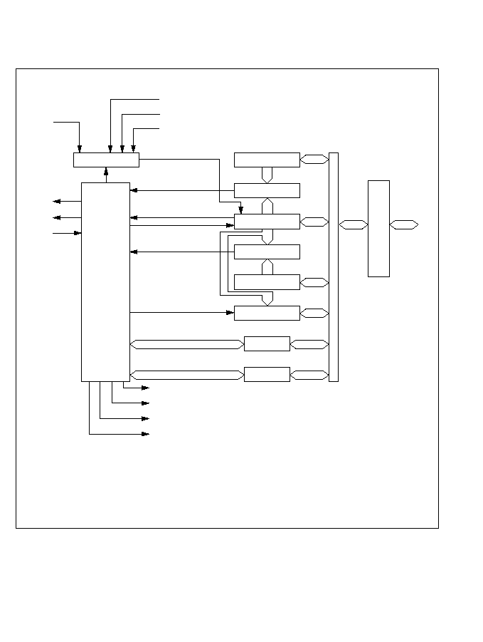
10.1.2. Block Diagram
Figure 10-1 shows a block diagram of one free-running timer channel.
ICI
OCIA
OCIB
FOVI
Interrupt signals
OCRA:
OCRB:
FRC:
ICR:
TCSR:
TCR:
Output Compare Register A
Output Compare Register B
Free Running Counter
Input Capture Register
Timer Control/Status Register
Timer Control Register
TCR
TCSR
ICR
OCRB
Comparator B
Capture
Compare-match B
Clear
Overflow
FRC
Comparator A
OCRA
Control
logic
FTOA
FTOB
FTI
FTCI
External clock
Internal clock
¯/4
¯/8
¯/32
Clock
Clock select
Compare-match A
Module
data
bus
Internal
data bus
Bus interface
Figure 10-1 Block Diagram of 16-Bit Free-Running Timer
178

10.1.3 Input and Output Pins
Table 10-1 lists the input and output pins of the free-running timer module.
Table 10-1 Input and Output Pins of Free-Running Timer Module
Channel Name
Abbreviation I/O
Function
1
Output compare A
FTOA
1
Output Output controlled by comparator A of FRT1
Output compare B or FTOB
1
/
Output / Output controlled by comparator B of FRT1,
counter clock input
FTCI
1
Input
or input of external clock source for FRT1
Input capture
FTI
1
Input
Trigger for capturing current count of FRT1
2
Output compare A
FTOA
2
Output Output controlled by comparator A of FRT2
Output compare B or FTOB
2
/
Output / Output controlled by comparator B of FRT2,
counter clock input
FTCI
2
Input
or input of external clock source for FRT2
Input capture
FTI
2
Input
Trigger for capturing current count of FRT2
3
Output compare A
FTOA
3
Output Output controlled by comparator A of FRT3
Output compare B or FTOB
3
/
Output / Output controlled by comparator B of FRT3,
counter clock input
FTCI
3
Input
or input of external clock source for FRT3
Input capture
FTI
3
Input
Trigger for capturing current count of FRT3
179

10.1.4 Register Configuration
Table 10-2 lists the registers of each free-running timer channel.
Table 10-2 Register Configuration
Initial
Channel
Name
Abbreviation
R/W
Value
Address
Timer control register
TCR
R/W
H'00
H'FF90
Timer control/status register
TCSR
R/(W)
*
H'00
H'FF91
Free-running counter (High)
FRC (H)
R/W
H'00
H'FF92
Free-running counter (Low)
FRC (L)
R/W
H'00
H'FF93
1
Output compare register A (High)
OCRA (H)
R/W
H'FF
H'FF94
Output compare register A (Low)
OCRA (L)
R/W
H'FF
H'FF95
Output compare register B (High)
OCRB (H)
R/W
H'FF
H'FF96
Output compare register B (Low)
OCRB (L)
R/W
H'FF
H'FF97
Input capture register (High)
ICR (H)
R
H'00
H'FF98
Input capture register (Low)
ICR (L)
R
H'00
H'FF99
Timer control register
TCR
R/W
H'00
H'FFA0
Timer control/status register
TCSR
R/(W)
*
H'00
H'FFA1
Free-running counter (High)
FRC (H)
R/W
H'00
H'FFA2
Free-running counter (Low)
FRC (L)
R/W
H'00
H'FFA3
2
Output compare register A (High)
OCRA (H)
R/W
H'FF
H'FFA4
Output compare register A (Low)
OCRA (L)
R/W
H'FF
H'FFA5
Output compare register B (High)
OCRB (H)
R/W
H'FF
H'FFA6
Output compare register B (Low)
OCRB (L)
R/W
H'FF
H'FFA7
Input capture register (High)
ICR (H)
R
H'00
H'FFA8
Input capture register (Low)
ICR (L)
R
H'00
H'FFA9
*
Software can write a "0" to clear bits 7 to 4, but cannot write a "1" in these bits.
180

Table 10-2 Register Configuration (cont)
Initial
Channel
Name
Abbreviation
R/W
Value
Address
Timer control register
TCR
R/W
H'00
H'FFB0
Timer control/status register
TCSR
R/(W)
*
H'00
H'FFB1
Free-running counter (High)
FRC (H)
R/W
H'00
H'FFB2
Free-running counter (Low)
FRC (L)
R/W
H'00
H'FFB3
3
Output compare register A (High)
OCRA (H)
R/W
H'FF
H'FFB4
Output compare register A (Low)
OCRA (L)
R/W
H'FF
H'FFB5
Output compare register B (High)
OCRB (H)
R/W
H'FF
H'FFB6
Output compare register B (Low)
OCRB (L)
R/W
H'FF
H'FFB7
Input capture register (High)
ICR (H)
R
H'00
H'FFB8
Input capture register (Low)
ICR (L)
R
H'00
H'FFB9
*
Software can write a "0" to clear bits 7 to 4, but cannot write a "1" in these bits.
10.2 Register Descriptions
10.2.1 Free-Running Counter (FRC)--H'FF92, H'FFA2, H'FFB2
Each FRC is a 16-bit readable/writable up-counter that increments on an internal pulse generated
from a clock source. The clock source is selected by the clock select 1 and 0 bits (CKS1 and
CKS0) of the timer control register (TCR).
The FRC can be cleared by compare-match A.
When the FRC overflows from H'FFFF to H'0000, the overflow flag (OVF) in the timer
control/status register (TCSR) is set to "1."
Because the FRC is a 16-bit register, a temporary register (TEMP) is used when the FRC is
written or read. See section 10.3, "CPU Interface" for details.
The FRCs are initialized to H'0000 at a reset and in the standby modes.
Bit
15
14
13
12
11
10
9
8
7
6
5
4
3
2
1
0
Initial value 0
0
0
0
0
0
0
0
0
0
0
0
0
0
0
0
Read/WriteR/W R/W R/W R/W R/W R/W R/W R/W R/W R/W R/W R/W R/W R/W R/W R/W
181

10.2.2 Output Compare Registers A and B (OCRA and OCRB)--H'FF94 and H'FF96,
H'FFA4 and H'FFA6, H'FFB4 and H'FFB6
OCRA and OCRB are 16-bit readable/writable registers, the contents of which are continually
compared with the value in the FRC. When a match is detected, the corresponding output
compare flag (OCFA or OCFB) is set in the timer control/status register (TCSR).
In addition, if the output enable bit (OEA or OEB) in the timer control register (TCR) is set to "1,"
when the output compare register and FRC values match, the logic level selected by the output
level bit (OLVLA or OLVLB) in the timer control status register (TCSR) is output at the output
compare pin (FTOA or FTOB).
The FTOA and FTOB output are "0" before the first compare-match.
Because OCRA and OCRB are 16-bit registers, a temporary register (TEMP) is used when they
are written. See section 10.3, "CPU Interface" for details.
OCRA and OCRB are initialized to H'FFFF at a reset and in the standby modes.
10.2.3 Input Capture Register (ICR)--H'FF98, H'FFA8, H'FFB8
The ICR is a 16-bit read-only register.
When the rising or falling edge of the signal at the input capture input pin is detected, the current
value of the FRC is copied to the ICR. At the same time, the input capture flag (ICF) in the timer
control/status register (TCSR) is set to "1." The input capture edge is selected by the input edge
select bit (IEDG) in the TCSR.
Because the ICR is a 16-bit register, a temporary register (TEMP) is used when the ICR is written
or read. See section 10.3, "CPU Interface" for details.
Bit
15
14
13
12
11
10
9
8
7
6
5
4
3
2
1
0
Initial value 1
1
1
1
1
1
1
1
1
1
1
1
1
1
1
1
Read/WriteR/W R/W R/W R/W R/W R/W R/W R/W R/W R/W R/W R/W R/W R/W R/W R/W
Bit
15
14
13
12
11
10
9
8
7
6
5
4
3
2
1
0
Initial value 0
0
0
0
0
0
0
0
0
0
0
0
0
0
0
0
Read/Write R
R
R
R
R
R
R
R
R
R
R
R
R
R
R
R
182

To ensure input capture, the pulse width of the input capture signal should be at least 1.5 system
clock periods (1.5∑¯).
The ICR is initialized to H'0000 at a reset and in the standby modes.
Note: When input capture is detected, the FRC value is transferred to the ICR even if the input
capture flag (ICF) is already set.
10.2.4 Timer Control Register (TCR)
The TCR is an 8-bit readable/writable register that selects the FRC clock source, enables the
output compare signals, and enables interrupts.
The TCR is initialized to H'00 at a reset and in the standby modes.
Bit 7--Input Capture Interrupt Enable (ICIE): This bit selects whether to request an input
capture interrupt (ICI) when the input capture flag (ICF) in the timer status/control register
(TCSR) is set to "1."
Bit 7
ICIE
Description
0
The input capture interrupt request (ICI) is disabled.
(Initial value)
1
The input capture interrupt request (ICI) is enabled.
Bit 6--Output Compare Interrupt Enable B (OCIEB): This bit selects whether to request
output compare interrupt B (OCIB) when output compare flag B (OCFB) in the timer
status/control register (TCSR) is set to "1."
¯
FTI
Minimum FTI Pulse Width
Bit
7
6
5
4
3
2
1
0
ICIE
OCIEB
OCIEA
OVIE
OEB
OEA
CKS1
CKS0
Initial value
0
0
0
0
0
0
0
0
Read/Write
R/W
R/W
R/W
R/W
R/W
R/W
R/W
R/W
183

Bit 6
OCIEB
Description
0
Output compare interrupt request B (OCIB) is disabled.
(Initial value)
1
Output compare interrupt request B (OCIB) is enabled.
Bit 5--Output Compare Interrupt Enable A (OCIEA): This bit selects whether to request
output compare interrupt A (OCIA) when output compare flag A (OCFA) in the timer
status/control register (TCSR) is set to "1."
Bit 5
OCIEA
Description
0
Output compare interrupt request A (OCIA) is disabled.
(Initial value)
1
Output compare interrupt request A (OCIA) is enabled.
Bit 4--Timer overflow Interrupt Enable (OVIE): This bit selects whether to request a free-
running timer overflow interrupt (FOVI) when the timer overflow flag (OVF) in the timer
status/control register (TCSR) is set to "1."
Bit 4
OVIE
Description
0
The free-running timer overflow interrupt request (FOVI) is disabled.
(Initial value)
1
The free-running timer overflow interrupt request (FOVI) is enabled.
Bit 3--Output Enable B (OEB): This bit selects whether to enable or disable output of the logic
level selected by the OLVLB bit in the timer status/control register (TCSR) at the output compare
B pin when the FRC and OCRB values match.
Bit 3
OEB
Description
0
Output compare B output is disabled.
(Initial value)
1
Output compare B output is enabled.
Bit 2--Output Enable A (OEA): This bit selects whether to enable or disable output of the logic
level selected by the OLVLA bit in the timer status/control register (TCSR) at the output compare
A pin when the FRC and OCRA values match.
184

Bit 2
OEA
Description
0
Output compare A output is disabled.
(Initial value)
1
Output compare A output is enabled.
Bits 1 and 0--Clock Select (CKS1 and CKS0): These bits select external clock input or one of
three internal clock sources for the FRC. External clock pulses are counted on the rising edge.
Bit 1
Bit 0
CKS1
CKS0
Description
0
0
Internal clock source (¯/4)
(Initial value)
0
1
Internal clock source (¯/8)
1
0
Internal clock source (¯/32)
1
1
External clock source (counted on the rising edge)
*
*
Output enable bit (bit 3) must be cleared to "0."
10.2.5 Timer Control/Status Register (TCSR)
The TCSR is an 8-bit readable and partially writable* register that selects the input capture edge
and output compare levels, and specifies whether to clear the counter on compare-match A. It also
contains four status flags.
The TCSR is initialized to H'00 at a reset and in the standby modes.
* Software can write a "0" in bits 7 to 4 to clear the flags, but cannot write a "1" in these bits.
Bit 7--Input Capture Flag (ICF): This status flag is set to "1" to indicate an input capture
event. It signifies that the FRC value has been copied to the ICR.
Bit
7
6
5
4
3
2
1
0
ICF
OCFB
OCFA
OVF
OLVLB
OLVLA
IEDG
CCLRA
Initial value
0
0
0
0
0
0
0
0
Read/Write
R/(W)
*
R/(W)
*
R/(W)
*
R/(W)
*
R/W
R/W
R/W
R/W
185

Bit 7
ICF
Description
0
This bit is cleared from 1 to 0 when: (Initial value)
1. The CPU reads the ICF bit, then writes a "0" in this bit.
2. The data transfer controller (DTC) serves an input capture interrupt.
1
This bit is set to 1 when an input capture signal causes the FRC value to be copied to the ICR.
Bit 6--Output Compare Flag B (OCFB): This status flag is set to "1" when the FRC value
matches the OCRB value.
Bit 6
OCFB
Description
0
This bit is cleared from 1 to 0 when: (Initial value)
1. The CPU reads the OCFB bit, then writes a "0" in this bit.
2. The data transfer controller (DTC) serves output compare interrupt B.
1
This bit is set to 1 when FRC = OCRB.
Bit 5--Output Compare Flag A (OCFA): This status flag is set to "1" when the FRC value
matches the OCRA value.
Bit 5
OCFA
Description
0
This bit is cleared from 1 to 0 when: (Initial value)
1. The CPU reads the OCFA bit, then writes a "0" in this bit.
2. The data transfer controller (DTC) serves output compare interrupt A.
1
This bit is set to 1 when FRC = OCRA.
Bit 4--Timer Overflow Flag (OVF): This status flag is set to "1" when the FRC overflows
(changes from H'FFFF to H'0000).
Bit 4
OVF
Description
0
This bit is cleared from 1 to 0 when the CPU reads (Initial value)
the OVF bit, then writes a "0" in this bit.
1
This bit is set to 1 when FRC changes from H'FFFF to H'0000.
Bit 3--Output Level B (OLVLB): This bit selects the logic level to be output at the FTOB pin
when the FRC and OCRB values match.
186

Bit 3
OLVLB
Description
0
A "0" logic level (Low) is output for compare-match B.
(Initial value)
1
A "1" logic level (High) is output for compare-match B.
Bit 2--Output Level A (OLVLA): This bit selects the logic level to be output at the FTOA pin
when the FRC and OCRA values match.
Bit 2
OLVLA
Description
0
A "0" logic level (Low) is output for compare-match A.
(Initial value)
1
A "1" logic level (High) is output for compare-match A.
Bit 1--Input Edge Select (IEDG): This bit selects whether to capture the count on the rising or
falling edge of the input capture signal.
Bit 1
IEDG
Description
0
The FRC value is copied to the ICR on the falling edge
(Initial value)
of the input capture signal.
1
The FRC value is copied to the ICR on the rising edge
of the input capture signal.
Bit 0--Counter Clear A (CCLRA): This bit selects whether to clear the FRC at compare-match
A (when the FRC and OCRA values match).
Bit 0
CCLRA
Description
0
The FRC is not cleared. (Initial value)
1
The FRC is cleared at compare-match A.
187

10.3 CPU Interface
The FRC, OCRA, OCRB, and ICR are 16-bit registers, but they are connected to an 8-bit data bus.
When the CPU accesses these four registers, to ensure that both bytes are written or read
simultaneously, the access is performed using an 8-bit temporary register (TEMP).
These registers are written and read as follows.
∑ Register Write
When the CPU writes to the upper byte, the upper byte of write data is placed in TEMP. Next,
when the CPU writes to the lower byte, this byte of data is combined with the byte in TEMP
and all 16 bits are written in the register simultaneously.
∑ Register Read
When the CPU reads the upper byte, the upper byte of data is sent to the CPU and the lower
byte is placed in TEMP. When the CPU reads the lower byte, it receives the value in TEMP.
Programs that access these four registers should normally use word access. Equivalently, they
may access first the upper byte, then the lower byte. Data will not be transferred correctly if the
bytes are accessed in reverse order, or if only one byte is accessed.
Coding Examples : Write the contents of R0 into OCRA in FRT1
MOV.W R0, @H'FF94
: Read ICR of FRT2
MOV.W, @H'FFA8, R0
The same considerations apply to access by the DTC.
Figure 10-2 shows the data flow when the FRC is accessed. The other registers are accessed in
the same way, except that when OCRA or OCRB is read, the upper and lower bytes are both
transferred directly to the CPU without using the temporary register.
188
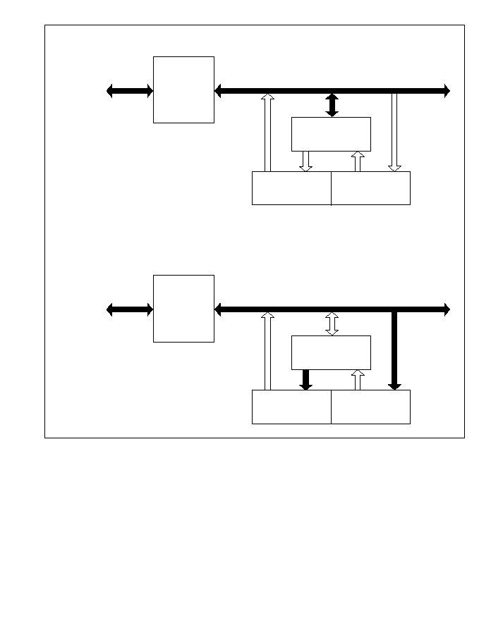
< Lower byte write >
CPU wites
data H'55
Bus interface
TEMP
[H'AA]
FRCH
[H'AA]
FRCL
[H'55]
Module data bus
< Upper byte write >
CPU wites
data H'AA
Bus interface
TEMP
[H'AA]
FRCH
[ ]
FRCL
[ ]
Module data bus
Figure 10-2 (a) Write Access to FRC (When CPU Writes H'AA55)
189

10.4 Operation
10.4.1 FRC Incrementation Timing
The FRC increments on a pulse generated once for each period of the selected (internal or
external) clock source.
If external clock input is selected, the FRC increments on the rising edge of the clock signal.
Figure 10-3 shows the increment timing.
< Lower byte read >
CPU wites
data H'55
Bus interface
TEMP
[H'55]
Module data bus
< Upper byte read >
CPU wites
data H'AA
Bus interface
TEMP
[H'55]
Module data bus
FRCH
[ ]
FRCL
[ ]
FRCH
[H'AA]
FRCL
[H'55]
Figure 10-2 (b) Read Access to FRC (When FRC Contains H'AA55)
190
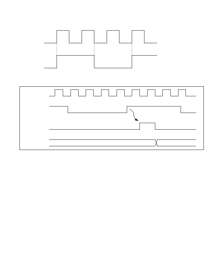
The pulse width of the external clock signal must be at least 1.5∑¯ clock periods. The counter will
not increment correctly if the pulse width is shorter than 1.5∑¯ clock periods.
10.4.2 Output Compare Timing
Setting of Output Compare Flags A and B (OCFA and OCFB): The output compare flags are
set to "1" by an internal compare-match signal generated when the FRC value matches the OCRA
or OCRB value. This compare-match signal is generated at the last state in which the two values
match, just before the FRC increments to a new value.
Accordingly, when the FRC and OCR values match, the compare-match signal is not generated
until the next period of the clock source. Figure 10-4 shows the timing of the setting of the output
compare flags.
¯
FTCI
Minimum FTCI Pulse Width
¯
External clock
source
FRC clock pulse
FRC
N
N + 1
Figure 10-3 Increment Timing for External Clock Input
191
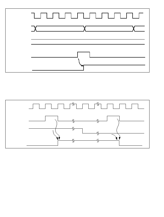
Output Timing: When a compare-match occurs, the logic level selected by the output level bit
(OLVLA or OLVLB) in the TCSR is output at the output compare pin (FTOA or FTOB).
Figure 10-5 shows the timing of this operation for compare-match A.
N
N
N + 1
ÿ
FRC
OCR
Internal compare-
match signal
OCF
¯
¯
FTOA
Internal compare-
match A signal
OLYLA
Figure 10-4 Setting of Output Compare Flags
Figure 10-5 Timing of Output Compare A
192
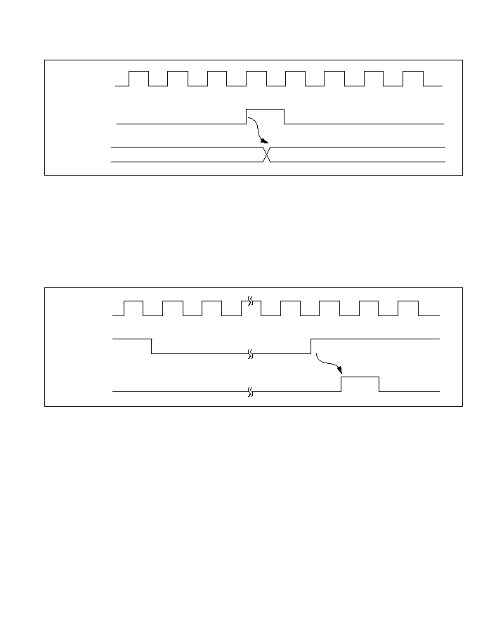
FRC Clear Timing: If the CCLRA bit is set to "1," the FRC is cleared when compare-match A
occurs. Figure 10-6 shows the timing of this operation.
10.4.3 Input Capture Timing
1. Input Capture Timing: An internal input capture signal is generated from the rising or falling
edge of the input at the input capture pin (FTI), as selected by the IEDG bit in the TCSR.
Figure 10-7 shows the usual input capture timing when the rising edge is selected
(IEDG = "1").
But if the upper byte of the ICR is being read when the input capture signal arrives, the internal
input capture signal is delayed by one state. Figure 10-8 shows the timing for this case.
Internal compare-
match A signal
FRC
¯
N
H'0000
Input at FTI pin
Internal input
capture signal
¯
Figure 10-6 Clearing of FRC by Compare-Match A
Figure 10-7 Input Capture Timing (Usual Case)
193
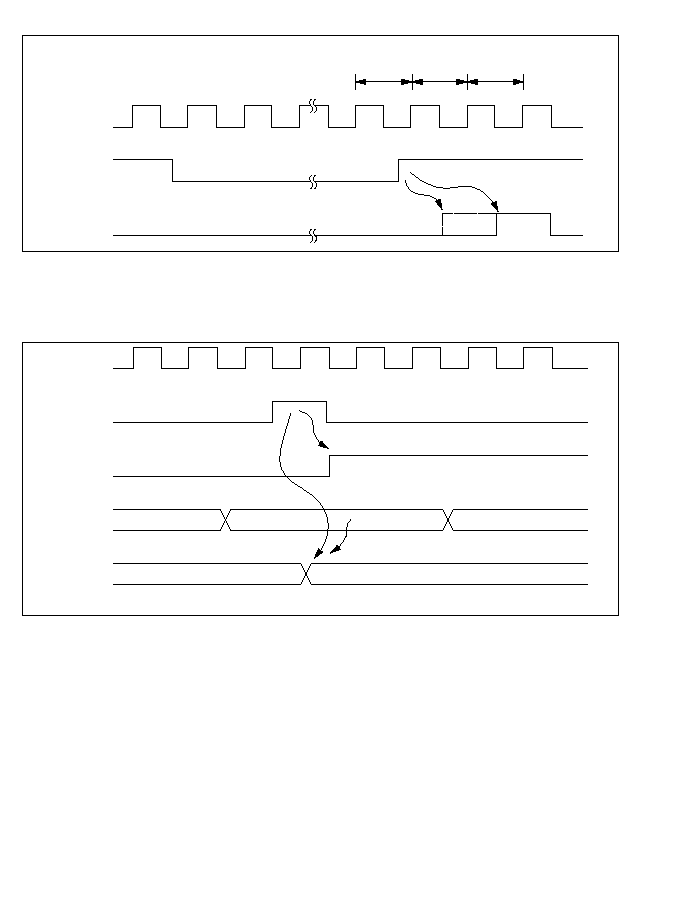
Timing of Input Capture Flag (ICF) Setting: The input capture flag (ICF) is set to "1" by the
internal input capture signal. Figure 10-9 shows the timing of this operation.
Read cycle: CPU reads upper byte of ICR
T
1
T
2
T
3
Input at FTI pin
Internal input
capture signal
¯
Internal input
capture signal
ICR
¯
ICF
FRC
N
N ≠ 1
N
N + 1
Figure 10-8 Input Capture Timing (1-State Delay)
Figure 10-9 Setting of Input Capture Flag
194
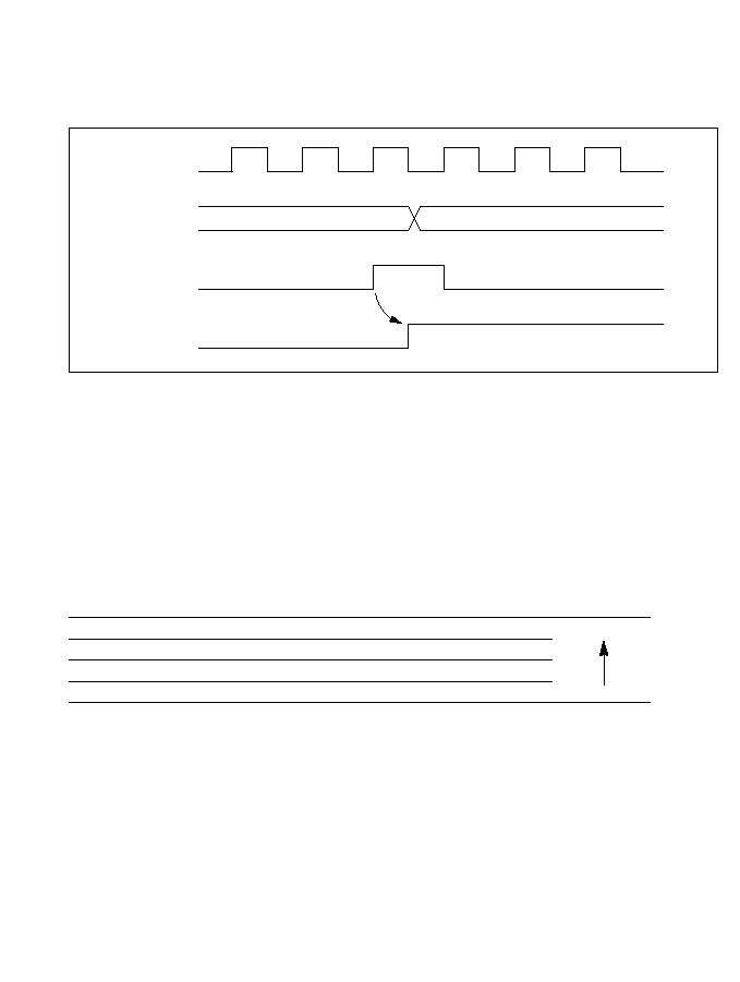
10.4.4 Setting of FRC Overflow Flag (OVF)
The FRC overflow flag (OVF) is set to "1" when the FRC overflows (changes from H'FFFF to
H'0000). Figure 10-10 shows the timing of this operation.
10.5 CPU Interrupts and DTC Interrupts
Each free-running timer channel can request four types of interrupts: input capture (ICI), output
compare A and B (OCIA and OCIB), and overflow (FOVI). Each interrupt is requested when the
corresponding enable and flag bits are set. Independent signals are sent to the interrupt controller
for each type of interrupt. Table 10-3 lists information about these interrupts.
Table 10-3 Free-Running Timer Interrupts
Interrupt
Description
DTC Service Available?
Priority
ICI
Requested when ICF is set
Yes
High
OCIA
Requested when OCFA is set
Yes
OCIB
Requested when OCFB is set
Yes
FOVI
Requested when OVF is set
No
Low
The ICI, OCIA, and OCIB interrupts can be directed to the data transfer controller (DTC) to have
a data transfer performed in place of the usual interrupt-handling routine.
When the DTC serves one of these interrupts, it automatically clears the ICF, OCFA, or OCFB
flag to "0." See section 6, "Data Transfer Controller" for further information on the DTC.
Internal overflow
signal
OVF
FRC
¯
H'FFFF
H'0000
Figure 10-10 Setting of Overflow Flag (OVF)
195

10.6 Synchronization of Free-Running Timers 1 to 3
10.6.1 Synchronization after a Reset
The three free-running timer channels are synchronized at a reset and remained synchronized
until:
∑ the clock source is changed;
∑ FRC contents are rewritten; or
∑ an FRC is cleared.
After a reset, each free-running counter operates on the ¯/4 internal clock source.
10.6.2 Synchronization by Writing to FRCs
When synchronization among free-running timers 1 to 3 is lost, it can be restored by writing to the
free-running counters.
Synchronization on Internal Clock Source: When an internal clock is selected, free-running
timers 1 to 3 can be synchronized by writing data to their free-running counters as indicated in
table 10-4.
Table 10-4 Synchronization by Writing to FRCs
Clock Source
Write Interval
Write Data
¯/4
4n + 1 (states)
m
(FRC1)
¯/8
8n + 1 (states)
m + n
(FRC2)
¯/32
32n + 1 (states)
m + 2n
(FRC3)
m, n: Arbitrary integers
After writing these data, synchronization can be checked by reading the three free-running
counters at the same interval as the write interval. If the read data have the same relative
differences as the write data, the three free-running timers are synchronized.
196

Example a: ¯/4 clock source, 12-state write interval (n = 3), on-chip memory
LA: LDC.B #H'FF,BR
; Initialize base register for short-format instruction (MOV:S)
LDC.W #H'0700,SR
; Raise interrupt mask level to 7
MOV.W #m,R1
; Data for free-running timer 1
MOV.W #m+3,R2
; Data for free-running timer 2 (m + n = m + 3)
MOV.W #m+6,R3
; Data for free-running timer 3 (m + 2n = m + 2
◊
3)
BSR SET4
; Call write routine
.ALIGN 2
; Align write instructions (MOV:S) at even address
SET4:MOV:S.W R1,@H'92:8
; Write to FRC 1 (address H'FF92)
9 states
BRN SET4:8
; 2-Byte dummy instruction
3 states
MOV:S.W R2,@H'A2:8
; Write to FRC 2 (address H'FFA2)
Total 12 states
BRN SET4:8
; 2-Byte dummy instruction
MOV:S.W R3,@H'B2:8
; Write to FRC 3 (address H'FFB2)
RTS
Example b: ¯/8 clock source, 16-state write interval (n = 2), on-chip memory
LB: LDC.B #H'FF,BR
LDC.W #H'0700,SR
MOV.W #m,R1
MOV.W #m+2,R2
MOV.W #m+4,R3
BSR SET8
.ALIGN 2
SET8:MOV:S.W R1,@H'92:8
; 9 States
BRN SET8:8
; 3 States
Total 16 states
XCH R1,R1
; 4 States
MOV:S.W R2,@H'A2:8
BRN SET8:8
XCH R2,R2
MOV:S.W R3,@H'B2:8
RTS
197

Example c: ¯/32 clock source, 32-state write interval (n = 1), on-chip memory
LC: LDC.B #H'FF,BR
LDC.W #H'0700,SR
MOV.W #m,R1
MOV.W #m+1,R2
MOV.W #m+2,R3
BSR SET32
.ALIGN 2
; Align on even address
SET32: MOV:S.W R1,@H'92:8
; 2 Bytes, 9 states
BSR WAIT:8
; 2 Bytes, 9 states
MOV:S.W R2,@H'A2:8
BSR WAIT:8
Total 32 states
MOV:S.W R3,@H'B2:8
RTS
.ALIGN 2
; Align on even address
WAIT: NOP
; 2 States
XCH R1,R1
; 4 States
RTS
; 8 States
Note: The stack is assumed to be in on-chip RAM.
Example d: ¯/4 clock source, 20-state write interval (n = 5), external memory
LD: LDC.B #H'FF,BR
LDC.W #H'0700,SR
; Set interrupt mask level to 7
CLR.B @H'F8:8
; Disable wait states
MOV.W #m,R1
MOV.W #m+5,R2
MOV.W #m+10,R3
MOV:S.W R1,@H'92:8
; 13 States
BRN LD:8
; 2 Bytes, 7 states
MOV:S.W R2,@H'A2:8
BRN LD:8
MOV:S.W R3,@H'B2:8
Total 20 states
198

Example e: ¯/8 clock source, 24-state write interval (n = 3), external memory
LE: LDC.B #H'FF,BR
LDC.W #H'0700,SR
CLR.B @H'F8"8
MOV.W #m,R1
MOV.W #m+3,R2
MOV.W #m+6,R3
MOV:S.W R1,@H'92:8
; 13 States
BRN LE:8
; 2 Bytes,
7 states
Total 24 states
NOP
; 1 Byte,
4 states
MOV:S.W R2,@H'A2:8
BRN LE:8
NOP
MOV:S.W R3,@H'B2:8
Example f: ¯/32 clock source, 32-state write interval (n = 1), external memory
LF: LDC.B #H'FF,BR
LDC.W #H'0700,SR
CLR.B @H'F8:8
MOV.W #m,R1
MOV.W #m+1,R2
MOV.W #m+2,R3
MOV:S.W R1,@H'92:8
; External memory, so 13 states
XCH R0,R0
;
8 states
BRN LF:8
; 2 Bytes,
7 states
NOP
;
4 states
MOV:S.W R2,@H'A2:8
XCH R0,R0
BRN LF:8
NOP
MOV:S.W R3,@H'B2:8
Total 32 states
199
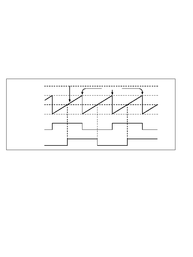
Synchronization on External Clock Source: When the external clock source is selected, the
free-running timers can be synchronized by halting their external clock inputs, then writing
identical values in their free-running counters.
10.7 Sample Application
In the example below, one free-running timer channel is used to generate two square-wave outputs
with a 50% duty factor and arbitrary phase relationship. The programming is as follows:
1. The CCLRA bit in the TCSR is set to "1."
2. Each time a compare-match interrupt occurs, software inverts the corresponding output level
bit in the TCSR.
10.8 Application Notes
Application programmers should note that the following types of contention can occur in the free-
running timers.
Contention between FRC Write and Clear: If an internal counter clear signal is generated
during the T
3
state of a write cycle to the lower byte of a free-running counter, the clear signal
takes priority and the write is not performed.
- - - - - -
- - - - - -
- - - - - -
- - - - - -
FRC
H'FFFF
OCRA
OCRB
H'0000
FTOA pin
FTOB pin
Clear counter
Figure 10-11 Square-Wave Output (Example)
200
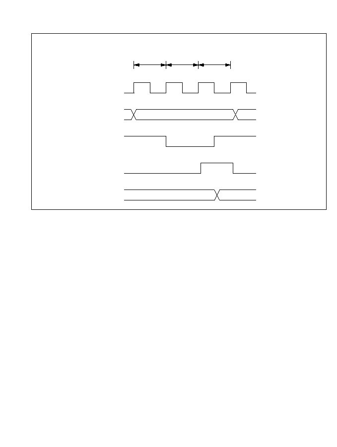
Figure 10-12 shows this type of contention.
Contention between FRC Write and Increment: If an FRC increment pulse is generated during
the T
3
state of a write cycle to the lower byte of a free-running counter, the write takes priority and
the FRC is not incremented.
Write cycle: CPU write to lower byte of FRC
T
1
T
2
T
3
Internal address bus
Internal write signal
FRC clear signal
¯
FRC
N
H'0000
FRC address
Figure 10-12 FRC Write-Clear Contention
201
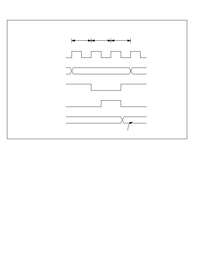
Figure 10-13 shows this type of contention.
Write cycle: CPU write to lower byte of FRC
T
1
T
2
T
3
Internal address bus
Internal write signal
FRC clock pulse
¯
FRC
N
M
FRC address
Write data
Figure 10-13 FRC Write-Increment Contention
202
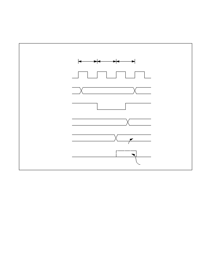
Contention between OCR Write and Compare-Match: If a compare-match occurs during the
T3 state of a write cycle to the lower byte of OCRA or OCRB, the write takes precedence and the
compare-match signal is inhibited.
Figure 10-14 shows this type of contention.
Incrementation Caused by Changing of Internal Clock Source: When an internal clock
source is changed, the changeover may cause the FRC to increment. This depends on the time at
which the clock select bits (CKS1 and CKS0) are rewritten, as shown in table 10-5.
The pulse that increments the FRC is generated at the falling edge of the internal clock source. If
clock sources are changed when the old source is High and the new source is Low, as in case No.
3 in table 10-5, the changeover generates a falling edge that triggers the FRC increment pulse.
Switching between an internal and external clock source can also cause the FRC to increment.
Write cycle: CPU write to lower byte of OCRA or OCRB
T
1
T
2
T
3
OCR address
N
N
N + 1
M
Write data
Inhibited
Compare-match
A or B signal
OCRA or OCRB
FRC
Internal write signal
Internal address bus
¯
Figure 10-14 Contention between OCR Write and Compare-Match
203
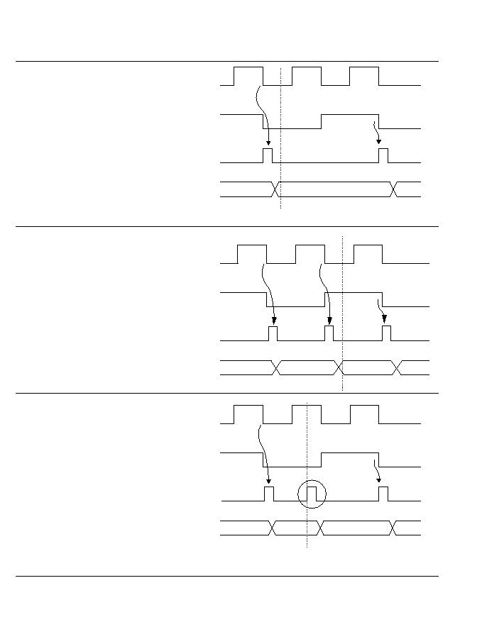
Table 10-5 Effect of Changing Internal Clock Sources
No.
Description
Timing Chart
1
Low
Low:
CKS1 and CKS0 are
rewritten while both
clock sources are Low.
2
Low
High:
CKS1 and CKS0 are
rewritten while old
clock source is Low and
new clock source is High.
3
High
Low:
CKS1 and CKS0 are
rewritten while old
clock source is High and
new clock source is Low.
The switching of clock sources is regarded as a falling edge that increments the FRC.
CKS rewrite
Old clock
source
New clock
source
FRC clock
pulse
FRC
N
N + 1
Old clock
source
New clock
source
FRC clock
pulse
FRC
N
N + 1
N + 2
CKS rewrite
Old clock
source
New clock
source
FRC clock
pulse
FRC
N
N + 1
N + 2
*
204
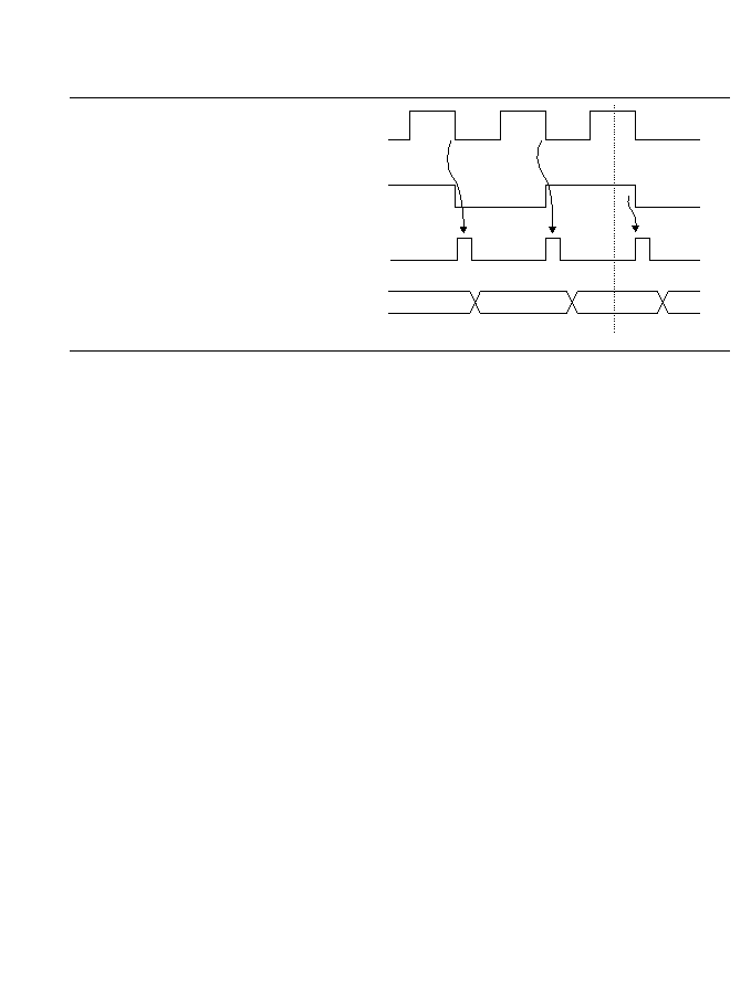
Table 10-5 Effect of Changing Internal Clock Sources (cont)
No.
Description
Timing Chart
4
High
High:
CKS1 and CKS0 are
rewritten while both
clock sources are High.
CKS rewrite
Old clock
source
New clock
source
FRC clock
pulse
FRC
N
N + 1
N + 2
205

Section 11 8-Bit Timer
11.1 Overview
The H8/532 chip includes a single 8-bit timer based on an 8-bit counter (TCNT). The timer has
two time constant registers (TCORA and TCORB) that are constantly compared with the TCNT
value to detect compare-match events. One application of the 8-bit timer is to generate a
rectangular-wave output with an arbitrary duty factor.
11.1.1 Features
The features of the 8-bit timer are listed below.
∑ Selection of four clock sources
The counter can be driven by an internal clock signal (¯/8, ¯/64, or ¯/1024) or an external clock
input (enabling use as an external event counter).
∑ Selection of three ways to clear the counter
The counter can be cleared on compare-match A or B, or by an external reset signal.
∑ Timer output controlled by two time constants
The single timer output (TMO) is controlled by two independent time constants, enabling the
timer to generate output waveforms with an arbitrary duty factor.
∑ Three types of interrupts
Compare-match A and B and overflow interrupts can be requested independently.
The compare match interrupts can be served by the data transfer controller (DTC), enabling
interrupt-driven data transfer with minimal CPU programming.
207
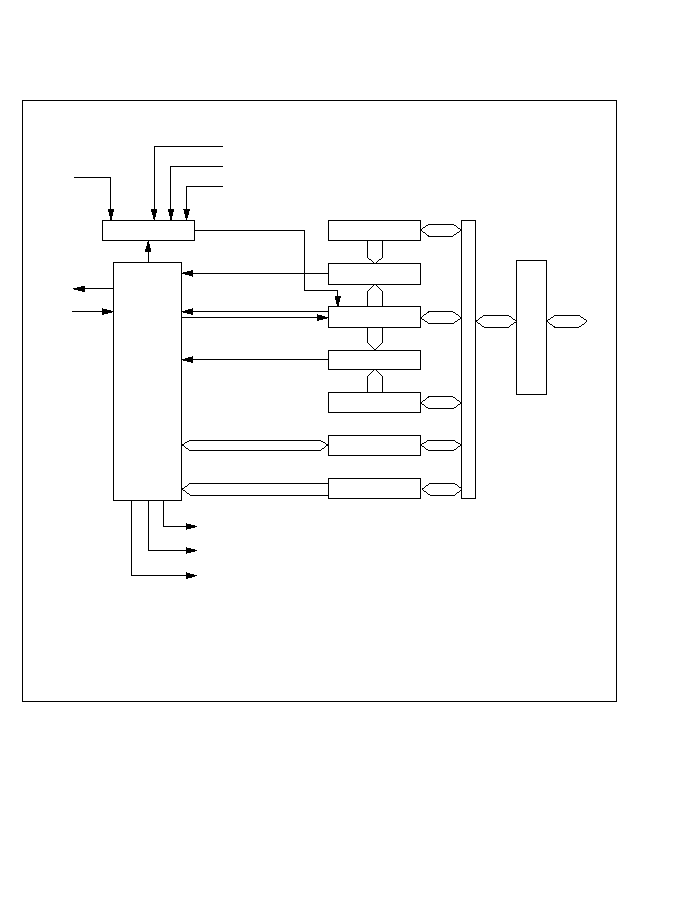
11.1.2 Block Diagram
Figure 11-1 shows a block diagram of 8-bit timer.
Compare-match B
Clear
Overflow
Clock
Compare-match A
Internal clocks
External clocks
TMCI
TMO
TMRI
Clock select
¯/8
¯/64
¯/1024
Control
logic
TCORA
Comparator A
TCNT
Comparator B
TCORB
TCSR
TCR
CMIA
CMIB
OVI
Interrupt signals
Bus interface
Module
data
bus
Internal
data bus
TCORA:
TCORB:
TCNT:
TCSR:
TCR:
Time Constant Register A
Time Constant Register B
Timer Counter
Timer Control/Status Register
Timer Control Register
Figure 11-1 Block Diagram of 8-Bit Timer
208

11.1.3 Input and Output Pins
Table 11-1 lists the input and output pins of the 8-bit timer.
Table 11-1 Input and Output Pins of 8-Bit Timer
Name
Abbreviation
I/O
Function
Timer output
TMO
Output
Output controlled by compare-match
Timer clock input
TMCI
Input
External clock source for the counter
Timer reset input
TMRI
Input
External reset signal for the counter
11.1.4 Register Configuration
Table 11-2 lists the registers of the 8-bit timer.
Table 11-2 8-Bit Timer Registers
Name
Abbreviation
R/W
Initial Value
Address
Timer control register
TCR
R/W
H'00
H'FFD0
Timer control/status register
TCSR
R/(W)
*
H'10
H'FFD1
Timer constant register A
TCORA
R/W
H'FF
H'FFD2
Timer constant register B
TCORB
R/W
H'FF
H'FFD3
Timer counter
TCNT
R/W
H'00
H'FFD4
*
Software can write a "0" to clear bits 7 to 5, but cannot write a "1" in these bits.
11.2 Register Descriptions
11.2.1 Timer Counter (TCNT)--H'FFD4
The timer counter (TCNT) is an 8-bit up-counter that increments on a pulse generated from one of
four clock sources. The clock source is selected by clock select bits 2 to 0 (CKS2 to CKS0) of the
timer control register (TCR). The CPU can always read or write the timer counter.
Bit
7
6
5
4
3
2
1
0
Initial value
0
0
0
0
0
0
0
0
Read/Write
R/W
R/W
R/W
R/W
R/W
R/W
R/W
R/W
209

The timer counter can be cleared by an external reset input or by an internal compare-match signal
generated at a compare-match event. Clock clear bits 1 and 0 (CCLR1 and CCLR0) of the timer
control register select the method of clearing.
When the timer counter overflows from H'FF to H'00, the overflow flag (OVF) in the timer
control/status register (TCSR) is set to "1."
The timer counter is initialized to H'00 at a reset and in the standby modes.
11.2.2 Time Constant Registers A and B (TCORA and TCORB)--H'FFD2 and H'FFD3
TCORA and TCORB are 8-bit readable/writable registers. The timer count is continually
compared with the constants written in these registers. When a match is detected, the
corresponding compare-match flag (CMFA or CMFB) is set in the timer control/status register
(TCSR).
The timer output signal (TMO) is controlled by these compare-match signals as specified by
output select bits 1 to 0 (OS1 to OS0) in the timer status/control register (TCSR).
TCORA and TCORB are initialized to H'FF at a reset and in the standby modes.
11.2.3 Timer Control Register (TCR)--H'FFD0
The TCR is an 8-bit readable/writable register that selects the clock source and the time at which
the timer counter is cleared, and enables interrupts.
The TCR is initialized to H'00 at a reset and in the standby modes.
Bit
7
6
5
4
3
2
1
0
Initial value
1
1
1
1
1
1
1
1
Read/Write
R/W
R/W
R/W
R/W
R/W
R/W
R/W
R/W
Bit
7
6
5
4
3
2
1
0
CMIEB
CMIEA
OVIE
CCLR1
CCLR0
CKS2
CKS1
CKS0
Initial value
0
0
0
0
0
0
0
0
Read/Write
R/W
R/W
R/W
R/W
R/W
R/W
R/W
R/W
210

Bit 7--Compare-match Interrupt Enable B (CMIEB): This bit selects whether to request
compare-match interrupt B (CMIB) when compare-match flag B (CMFB) in the timer
status/control register (TCSR) is set to "1."
Bit 7
CMIEB
Description
0
Compare-match interrupt request B (CMIB) is disabled.
(Initial value)
1
Compare-match interrupt request B (CMIB) is enabled.
Bit 6--Compare-match Interrupt Enable A (CMIEA): This bit selects whether to request
compare-match interrupt A (CMIA) when compare-match flag A (CMFA) in the timer
status/control register (TCSR) is set to "1."
Bit 6
CMIEA
Description
0
Compare-match interrupt request A (CMIA) is disabled.
(Initial value)
1
Compare-match interrupt request A (CMIA) is enabled.
Bit 5--Timer Overflow Interrupt Enable (OVIE): This bit selects whether to request a timer
overflow interrupt (OVI) when the overflow flag (OVF) in the timer status/control register (TCSR)
is set to "1."
Bit 5
OVIE
Description
0
The timer overflow interrupt request (OVI) is disabled.
(Initial value)
1
The timer overflow interrupt request (OVI) is enabled.
Bits 4 and 3--Counter Clear 1 and 0 (CCLR1 and CCLR0): These bits select how the timer
counter is cleared: by compare-match A or B or by an external reset input.
Bit 4
Bit 3
CCLR1
CCLR0
Description
0
0
Not cleared.
(Initial value)
0
1
Cleared on compare-match A.
1
0
Cleared on compare-match B.
1
1
Cleared on rising edge of external reset input signal.
211

Bits 2, 1, and 0--Clock Select (CKS2, CKS1, and CKS0): These bits select the internal or
external clock source for the timer counter. For the external clock source they select whether to
increment the count on the rising or falling edge of the clock input, or on both edges.
Bit 2
Bit 1
Bit 0
CKS2
CKS1
CKS0
Description
0
0
0
No clock source (timer stopped).
(Initial value)
0
0
1
Internal clock source (¯/8).
0
1
0
Internal clock source (¯/64).
0
1
1
Internal clock source (¯/1024).
1
0
0
No clock source (timer stopped).
1
0
1
External clock source, counted on the rising edge.
1
1
0
External clock source, counted on the falling edge.
1
1
1
External clock source, counted on both the rising
and falling edges.
11.2.4 Timer Control/Status Register (TCSR)
The TCSR is an 8-bit readable and partially writable* register that indicates compare-match and
overflow status and selects the effect of compare-match events on the timer output signal (TMO).
The TCSR is initialized to H'10 at a reset and in the standby modes.
* Software can write a "0" in bits 7 to 5 to clear the flags, but cannot write a "1" in these bits.
Bit 7--Compare-Match Flag B (CMFB): This status flag is set to "1" when the timer count
matches the time constant set in TCORB.
Bit
7
6
5
4
3
2
1
0
CMFB
CMFA
OVF
--
OS3
OS2
OS1
OS0
Initial value
0
0
0
1
0
0
0
0
Read/Write
R/(W)
*
R/(W)
*
R/(W)
*
--
R/W
R/W
R/W
R/W
212

Bit 7
CMFB
Description
0
This bit is cleared from 1 to 0 when:
(Initial value)
1. The CPU reads the CMFB bit, then writes a "0" in this bit.
2. Compare-match interrupt B is served by the data transfer controller (DTC).
1
This bit is set to 1 when TCNT = TCORB.
Bit 6--Compare-Match Flag A (CMFA): This status flag is set to "1" when the timer count
matches the time constant set in TCORA.
Bit 6
CMFA
Description
0
This bit is cleared from 1 to 0 when:
(Initial value)
1. The CPU reads the CMFA bit, then writes a "0" in this bit.
2. Compare-match interrupt A is served by the data transfer controller (DTC).
1
This bit is set to 1 when TCNT = TCORA.
Bit 5--Timer Overflow Flag (OVF): This status flag is set to "1" when the timer count
overflows (changes from H'FF to H'00).
Bit 5
OVF
Description
0
This bit is cleared from 1 to 0 when the CPU reads (Initial value)
the OVF bit, then writes a "0" in this bit.
1
This bit is set to 1 when TCNT changes from H'FF to H'00.
Bit 4--Reserved: This bit cannot be modified and is always read as "1."
Bits 3 to 0--Output Select 3 to 0 (OS3 to OS0): These bits specify the effect of compare-match
events on the timer output signal (TMO). Bits OS3 and OS2 control the effect of compare-match B
on the output level. Bits OS1 and OS0 control the effect of compare-match A on the output level.
When all four output select bits are cleared to "0" the TMO signal is not output. The TMO output
is "0" before the first compare-match.
Bit 3
Bit 2
OS3
OS2
Description
0
0
No change when compare-match B occurs.
(Initial value)
0
1
Output changes to "0" when compare-match B occurs.
1
0
Output changes to "1" when compare-match B occurs.
1
1
Output inverts (toggles) when compare-match B occurs.
213
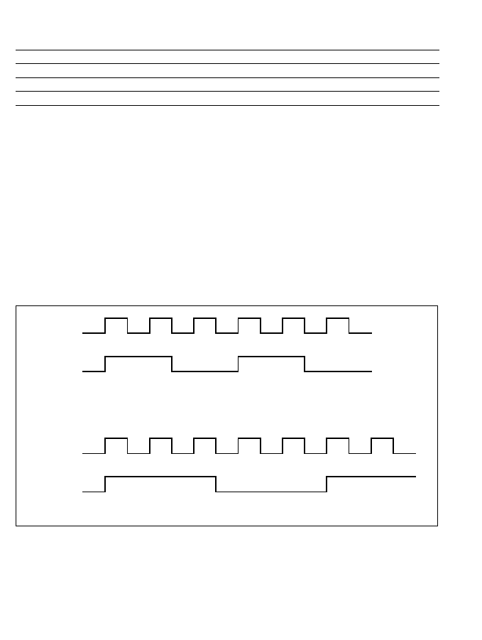
Bit 1
Bit 0
OS1
OS0
Description
0
0
No change when compare-match A occurs. (Initial value)
0
1
Output changes to "0" when compare-match A occurs.
1
0
Output changes to "1" when compare-match A occurs.
1
1
Output inverts (toggles) when compare-match A occurs.
11.3 Operation
11.3.1 TCNT Incrementation Timing
The timer counter increments on a pulse generated once for each period of the selected (internal or
external) clock source.
If external clock input (TMCI) is selected, the timer counter can increment on the rising edge, the
falling edge, or both edges of the external clock signal.
The external clock pulse width must be at least 1.5∑¯ clock periods for incrementation on a single
edge, and at least 2.5∑¯ clock periods for incrementation on both edges. The counter will not
increment correctly if the pulse width is shorter than these values.
¯
TMCI
Minimum TMCI Pulse Width
(Single-Edge Incrementation)
¯
TMCI
Minimum TMCI Pulse Width
(Double-Edge Incrementation)
214
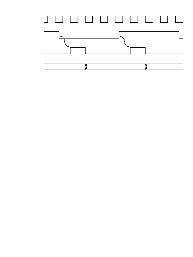
11.3.2 Compare Match Timing
Setting of Compare-Match Flags A and B (CMFA and CMFB): The compare-match flags are
set to "1" by an internal compare-match signal generated when the timer count matches the time
constant in TCORA or TCORB. The compare-match signal is generated at the last state in which
the match is true, just before the timer counter increments to a new value.
Accordingly, when the timer count matches one of the time constants, the compare-match signal is
not generated until the next period of the clock source. Figure 11-3 shows the timing of the
setting of the compare-match flags.
External clock
source
TCNT clock
pulse
TCNT
N
N + 1
ÿ
N ≠ 1
¯
External clock
source
TCNT clock
pulse
TCNT
Figure 11-2 Count Timing for External Clock Input
215
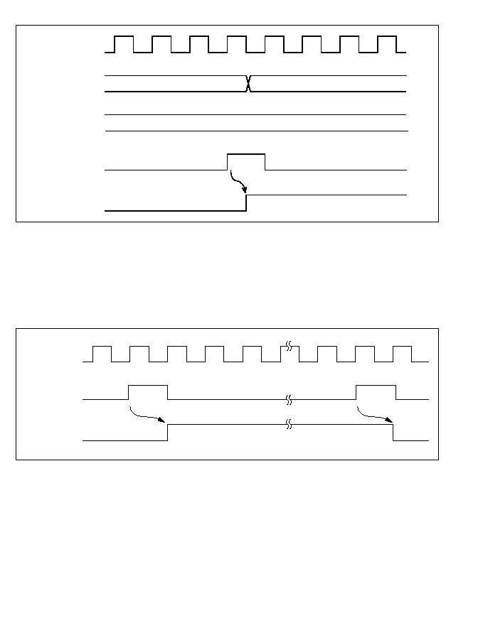
Output Timing: When a compare-match event occurs, the timer output (TMO) changes as
specified by the output select bits (OS3 to OS0) in the TCSR. Depending on these bits, the output
can remain the same, change to "0," change to "1," or toggle.
Figure 11-4 shows the timing when the output is set to toggle on compare-match A.
ÿ
TCNT
TCOR
Internal
compare-match
signal
CMF
N
N + 1
N
¯
Internal
compare-match
A signal
¯
Timer output
(TMO)
Figure 11-3 Setting of Compare-Match Flags
Figure 11-4 Timing of Timer Output
216
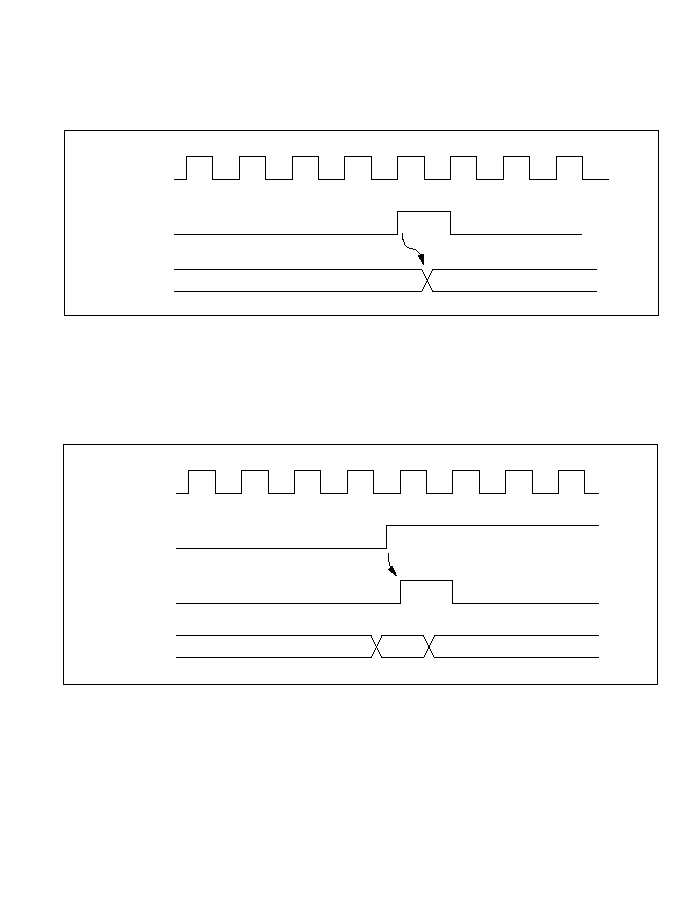
Timing of Compare-Match Clear
Depending on the CCLR1 and CCLR0 bits in the TCR, the timer counter can be cleared when
compare-match A or B occurs. Figure 11-5 shows the timing of this operation.
11.3.3 External Reset of TCNT
When the CCLR1 and CCLR0 bits in the TCR are both set to "1," the timer counter is cleared on
the rising edge of an external reset input. Figure 11-6 shows the timing of this operation.
N
H'00
Internal
compare-match
signal
TCNT
¯
H'00
N ≠ 1
N
TCNT
Internal clear
pulse
External reset
input (TMRI)
¯
Figure 11-5 Timing of Compare-Match Clear
Figure 11-6 Timing of External Reset
217

11.3.4 Setting of TCNT Overflow Flag
The overflow flag (OVF) is set to "1" when the timer count overflows (changes from H'FF to
H'00). Figure 11-7 shows the timing of this operation.
11.4 CPU Interrupts and DTC Interrupts
The 8-bit timer can generate three types of interrupts: compare-match A and B (CMIA and
CMIB), and overflow (OVI). Each interrupt is requested when the corresponding enable and flag
bits are set in the TCR and TCSR. Independent signals are sent to the interrupt controller for each
type of interrupt. Table 11-3 lists information about these interrupts.
Table 11-3 8-Bit Timer Interrupts
Interrupt
Description
DTC Service Available?
Priority
CMIA
Requested when CMFA is set
Yes
High
CMIB
Requested when CMFB is set
Yes
OVI
Requested when OVF is set
No
Low
The CMIA and CMIB interrupts can be served by the data transfer controller (DTC) to have a data
transfer performed.
When the DTC serves one of these interrupts, it automatically clears the CMFA or CMFB flag to
"0." See section 6, "Data Transfer Controller" for further information on the DTC.
ÿ
H'00
TCNT
Internal overflow
signal
OVF
H'FF
¯
Figure 11-7 Setting of Overflow Flag (OVF)
218
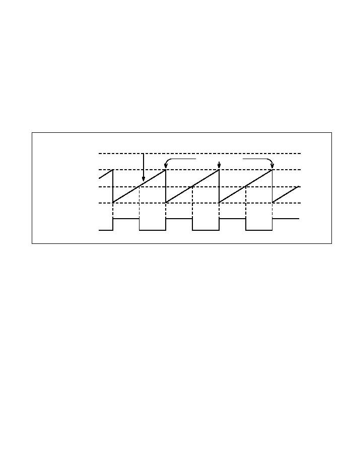
11.5 Sample Application
In the example below, the 8-bit timer is used to generate a pulse output with a selected duty factor.
The control bits are set as follows:
1. In the TCR, CCLR1 is cleared to "0" and CCLR0 is set to "1" so that the timer counter is
cleared when its value matches the constant in TCORA.
2. In the TCSR, bits OS3 to OS0 are set to "0110," causing the output to change to "1" on
compare-match A and to "0" on compare-match B.
With these settings, the 8-bit timer provides output of pulses at a rate determined by TCORA with
a pulse width determined by TCORB. No software intervention is required.
Clear counter
TCNT
H'FF
TCORA
TCORB
H'00
TMO pin
Figure 11-8 Example of Pulse Output
219
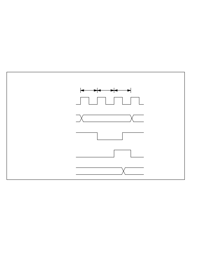
11.6 Application Notes
Application programmers should note that the following types of contention can occur in the 8-bit
timer.
Contention between TCNT Write and Clear: If an internal counter clear signal is generated
during the T
3
state of a write cycle to the timer counter, the clear signal takes priority and the write
is not performed.
Figure 11-9 shows this type of contention.
TCNT address
N
H'00
Internal Address
bus
Internal write
signal
¯
Counter clear
signal
TCNT
Write cycle: CPU writes to TCNT
T
1
T
2
T
3
Figure 11-9 TCNT Write-Clear Contention
220
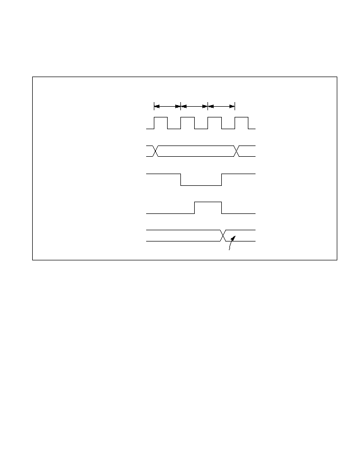
Contention between TCNT Write and Increment: If a timer counter increment pulse is
generated during the T
3
state of a write cycle to the timer counter, the write takes priority and the
timer counter is not incremented.
Figure 11-10 shows this type of contention.
TCNT address
N
M
Write data
Internal Address
bus
Internal write
signal
¯
TCNT clock
pulse
TCNT
Write cycle: CPU writes to TCNT
T
1
T
2
T
3
Figure 11-10 TCNT Write-Increment Contention
221
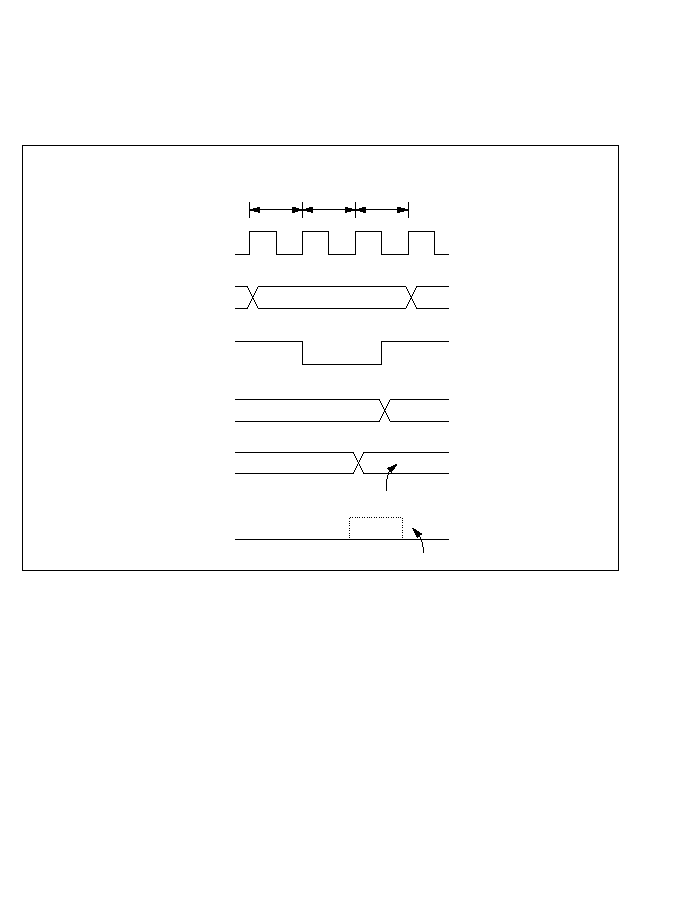
Contention between TCOR Write and Compare-Match: If a compare-match occurs during the
T
3
state of a write cycle to TCORA or TCORB, the write takes precedence and the compare-
match signal is inhibited.
Figure 11-11 shows this type of contention.
Contention between Compare-Match A and Compare-Match B: If identical time constants
are written in TCORA and TCORB, causing compare-match A and B to occur simultaneously,
any conflict between the output selections for compare-match A and B is resolved by following
the priority order in table 11-4.
TCNT address
N
N + 1
N
M
Write cycle: CPU writes to TCORA
or TCORB
T
1
T
2
T
3
TCOR write
data
Inhibited
Internal address
bus
¯
Internal write
signal
TCNT
TCORA or
TCORB
Compare-match
A or B signal
Figure 11-11 Contention between TCOR Write and Compare-Match
222

Table 11-4 Priority Order of Timer Output
Output Selection
Priority
Toggle
High
"1" Output
"0" Output
No change
Low
Incrementation Caused by Changing of Internal Clock Source: When an internal clock
source is changed, the changeover may cause the timer counter to increment. This depends on the
time at which the clock select bits (CKS2 to CKS0) are rewritten, as shown in table 11-5.
The pulse that increments the timer counter is generated at the falling edge of the internal clock
source signal. If clock sources are changed when the old source is High and the new source is
Low, as in case No. 3 in table 11-5, the changeover generates a falling edge that triggers the
TCNT clock pulse and increments the timer counter.
Switching between an internal and external clock source can also cause the timer counter to
increment.
Table 11-5 Effect of Changing Internal Clock Sources
No.
Description
Timing Chart
1
Low
Low
*
1
:
CKS1 and CKS0 are
rewritten while both
clock sources are Low.
Note:
*
1 Including a transition from Low to the stopped state (CKS1 = 0, CKS0 = 0), or a
transition from the stopped state to Low.
CKS rewrite
Old clock
source
TCNT clock
pulse
New clock
source
TCNT
N
N + 1
223
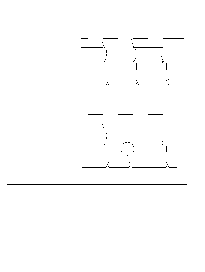
Table 11-5 Effect of Changing Internal Clock Sources (cont)
No.
Description
Timing Chart
2
Low
High
*
1
:
CKS1 and CKS0 are
rewritten while old
clock source is Low and
new clock source is High.
3
High
Low
*
2
:
CKS1 and CKS0 are
rewritten while old
clock source is High and
new clock source is Low.
Note:
*
1 Including a transition from the stopped state to High.
*
2 Including a transition from High to the stopped state.
*
3 The switching of clock sources is regarded as a falling edge that increments the TCNT.
CKS rewrite
Old clock
source
New clock
source
TCNT clock
pulse
TCNT
N
N + 1
N + 2
CKS rewrite
Old clock
source
New clock
source
TCNT clock
pulse
TCNT
N
N + 1
N + 2
*
3
224
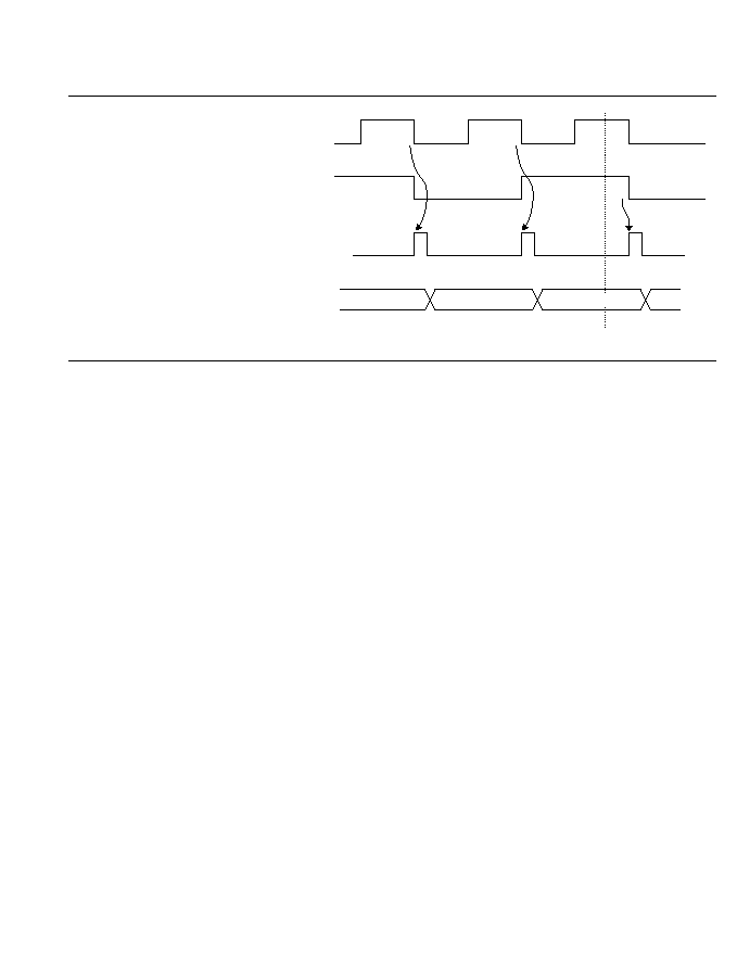
Table 11-5 Effect of Changing Internal Clock Sources (cont)
No.
Description
Timing Chart
4
High
High:
CKS1 and CKS0 are
rewritten while both
clock sources are High.
CKS rewrite
Old clock
source
New clock
source
TCNT clock
pulse
TCNT
N
N + 1
N + 2
225

Section 12 PWM Timer
12.1 Overview
The H8/532 has an on-chip pulse-width modulation (PWM) timer module with three independent
channels (PWM1, PWM2, and PWM3). All three channels are functionally identical. Using an
8-bit timer counter, each PWM channel generates a rectangular output pulse with a duty factor of
0 to 100%. The duty factor is specified in an 8-bit duty register (DTR).
12.1.1 Features
The PWM timer module has the following features:
∑ Selection of eight clock sources
∑ Duty factors from 0 to 100% with 1/250 resolution
∑ Output with positive or negative logic
12.1.2 Block Diagram
Figure 12-1 shows a block diagram of one PWM timer channel.
227

12.1.3 Input and Output Pins
Table 12-1 lists the output pins of the PWM timer module. There are no input pins.
Table 12-1 Output Pins of PWM Timer Module
Name
Abbreviation
I/O
Function
PWM1 output
PW
1
Output
Pulse output from PWM timer channel 1.
PWM2 output
PW
2
Output
Pulse output from PWM timer channel 2.
PWM3 output
PW
3
Output
Pulse output from PWM timer channel 3.
DTR:
TCNT:
TCR:
Duty Register
Timer Counter
Timer Control Register
Clock
Clock
select
Internal clock source
¯/2
¯/8
¯/32
¯/128
¯/256
¯/1024
¯/2048
¯/4096
Bus interface
Internal
data bus
Module
data bus
TCR
PW
DTR
TCNT
Comparator
Output
control
Compare-
match
Figure 12-1 Block Diagram of PWM Timer
228

12.1.4 Register Configuration
The PWM timer module has three registers for each channel as listed in table12-2.
Table 12-2 PWM Timer Registers
Initial
Channel
Name
Abbreviation
R/W
Value
Address
1
Timer control register
TCR
R/W
H'38
H'FFC0
Duty register
DTR
R/W
H'FF
H'FFC1
Timer counter
TCNT
R/(W)
*
H'00
H'FFC2
2
Timer control register
TCR
R/W
H'38
H'FFC4
Duty register
DTR
R/W
H'FF
H'FFC5
Timer counter
TCNT
R/(W)
*
H'00
H'FFC6
3
Timer control register
TCR
R/W
H'38
H'FFC8
Duty register
DTR
R/W
H'FF
H'FFC9
Timer counter
TCNT
R/(W)
*
H'00
H'FFCA
*
The timer counters are read/write registers, but the write function is for test purposes only.
Application programs should never write to these registers.
12.2 Register Descriptions
12.2.1 Timer Counter (TCNT)--H'FFC2, H'FFC4, H'FFCA
The PWM timer counters (TCNT) are 8-bit up-counters. When the output enable bit (OE) in the
timer control register (TCR) is set to 1, the timer counter starts counting pulses of an internal
clock source selected by clock select bits 2 to 0 (CKS2 to CKS0). After counting from H'00 to
H'F9, the timer counter repeats from H'00.
The PWM timer counters can be read and written, but the write function is for test purposes only.
Application software should never write to a PW timer counter, because this may have
unpredictable effects.
Bit
7
6
5
4
3
2
1
0
Initial value
0
0
0
0
0
0
0
0
Read/Write
R/W
R/W
R/W
R/W
R/W
R/W
R/W
R/W
229

The PWM timer counters are initialized to H'00 at a reset and in the standby modes, and when the
OE bit is cleared to 0.
12.2.2 Duty Register (DTR)--H'FFC1, H'FFC5, H'FFC9
The duty registers (DTR) specify the duty factor of the output pulse. Any duty factor from 0 to
100% can be selected, with a resolution of 1/250. Writing 0 (H'00) in a DTR gives a 0% duty
factor; writing 125 (H'7D) gives a 50% duty factor; writing 250 (H'FA) gives a 100% duty factor.
The timer count is continually compared with the DTR contents. If the DTR value is not 0, when
the count increments from H'00 to H'01 the PWM output signal is set to 1. When the count
increments to the DTR value, the PWM output returns to 0. If the DTR value is 0 (duty factor
0%), the PWM output remains constant at 0.
The DTRs are double-buffered. A new value written in a DTR while the timer counter is running
does not become valid until after the count changes from H'F9 to H'00. When the timer counter is
stopped (while the OE bit is 0), new values become valid as soon as written. When a DTR is
read, the value read is the currently valid value.
The DTRs are initialized to H'FF at a reset and in the standby modes.
12.2.3 Timer Control Register (TCR)--H'FFC0, H'FFC4, H'FFC8
The TCRs are 8-bit readable/writable registers that select the clock source and control the PWM
outputs.
The TCRs are initialized to H'38 at a reset and in the standby modes.
Bit
7
6
5
4
3
2
1
0
Initial value
1
1
1
1
1
1
1
1
Read/Write
R/W
R/W
R/W
R/W
R/W
R/W
R/W
R/W
Bit
7
6
5
4
3
2
1
0
OE
OS
--
--
--
CKS2
CKS1
CKS0
Initial value
0
0
1
1
1
0
0
0
Read/Write
R/W
R/W
--
--
--
R/W
R/W
R/W
230

Bit 7--Output Enable (OE): This bit enables the timer counter and the PWM output.
Bit 7
OE
Description
0
PWM output is disabled. TCNT is cleared to H'00 and stopped. (Initial value)
1
PWM output is enabled. TCNT runs.
Bit 6--Output Select (OS): This bit selects positive or negative logic for the PWM output.
Bit 6
OS
Description
0
Positive logic; positive-going PWM pulse, 1 = High
(Initial value)
1
Negative logic; negative-going PWM pulse, 1 = Low
Bits 5 to 3--Reserved: These bits cannot be modified and are always read as 1.
Bits 2, 1, and 0--Clock Select (CKS2, CKS1, and CKS0): These bits select one of eight clock
sources obtained by dividing the system clock (¯).
Bit 2
Bit 1
Bit 0
CKS2
CKS1
CKS0
Description
0
0
0
¯/2 (Initial value)
0
0
1
¯/8
0
1
0
¯/32
0
1
1
¯/128
1
0
0
¯/256
1
0
1
¯/1024
1
1
0
¯/2048
1
1
1
¯/4096
From the clock source frequency, the resolution, period, and frequency of the PWM output can be
calculated as follows.
Resolution
= 1/clock source frequency
PWM period
= resolution
◊
250
PWM frequency = 1/PWM period
If the ¯ clock frequency is 10MHz, then the resolution, period, and frequency of the PWM output
for each clock source are given in table12-3.
231

Table 12-3 PWM Timer Parameters for 10MHz System Clock
12.3 Operation
Figure 12-2 shows the timing of the PWM timer operation.
1. Positive Logic (OS = "0")
(1) When OE = "0"--(a) in figure 12-2: The timer count is held at H'00 and PWM output is
inhibited. (The pin is used for port 9 input/output, and its state depends on the corresponding
port 9 data register and data direction register.) Any value (such as N in figure 12-2) written
in the DTR becomes valid immediately.
(2) When OE = "1"
i) The timer counter begins incrementing, and the PWM output goes High. [(b) in figure 12-2]
ii) When the count reaches the DTR value, the PWM output goes Low. [(c) in figure 12-2]
iii)If the DTR value is changed (by writing the data "M" in figure 12-2), the new value
becomes valid after the timer count changes from H'F9 to H'00. [(d) in figure 12-2]
2. Negative Logic (OS = "1"): The operation is the same except that High and Low are reversed
in the PWM output. [(e) in figure 12-2]
Internal Clock Frequency
Resolution
PWM Period
PWM Frequency
¯/2
200ns
50µs
20kHz
¯/8
800ns
200µs
5kHz
¯/32
3.2µs
800µs
1.25kHz
¯/128
12.8µs
3.2ms
312.5Hz
¯/256
25.6µs
6.4ms
156.3Hz
¯/1024
102.4µs
25.6ms
39.1Hz
¯/2048
204.8µs
51.2ms
19.5Hz
¯/4096
409.6µs
102.4ms
9.8Hz
232
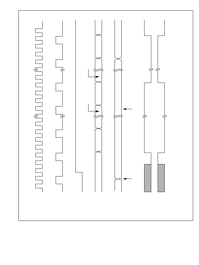
TCNT clock
pulses
¯
OE
TCNT
(OS = "0")
DTR
PWM output
(OS = "1")
* Used for port 9 input/output: state depends on values in data register and data direction register.
H'FF
(d) M
N written in DTR
*
*
(b)
(a)
(e)
(a) H'00
M written in DTR
(b) H'01
H'02
N ≠ 1
N
+ 1
N
N
H'F9
(c)
(c)
(d) H'00
H'01
Figure 12-2 PWM Timing
233

12.4 Application Notes
Two notes on the use of the PWM timer module are given below.
1. Any necessary changes to the clock select bits (CKS2 to CKS0) and output select bit (OS)
should be made before the output enable bit (OE) is set to 1.
2. If the DTR value is H'00, the duty factor is 0% and PWM output remains constant at 0. If the
DTR value is H'FA to H'FF, the duty factor is 100% and PWM output remains constant at 1.
(For positive logic, 0 is Low and 1 is High. For negative logic, 0 is High and 1 is Low.)
234

Section 13 Watchdog Timer
13.1 Overview
The H8/532 has an on-chip watchdog timer (WDT) module. This module can monitor system
operation by requesting a nonmaskable interrupt if a system crash allows the timer count to
overflow.
When this watchdog function is not needed, the WDT module can be used as an interval timer. In
the interval timer mode, an IRQ
0
interrupt is requested at each counter overflow.
The WDT module is also used in recovering from the software standby mode.
13.1.1 Features
The basic features of the watchdog timer module are summarized as follows:
∑ Selection of eight clock sources
∑ Selection of two modes: watchdog timer mode and interval timer mode
∑ Counter overflow generates an interrupt request
NMI request in the watchdog timer mode; IRQ
0
request in the interval timer mode.
235
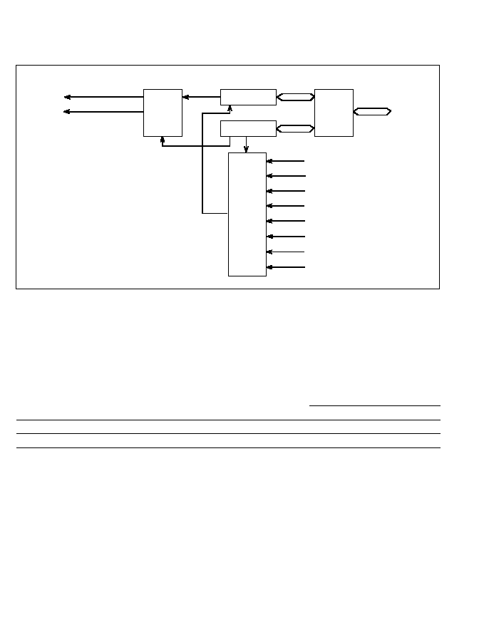
13.1.2 Block Diagram
Figure 13-1 is a block diagram of the watchdog timer.
13.1.3 Register Configuration
Table 13-1 lists information on the watchdog timer registers.
Table 13-1 Register Configuration
Initial
Addresses
Name
Abbreviation
R/W
Value
Write
Read
Timer control/status register
TCSR
R/(W)
*
H'18
H'FFED
H'FFEC
Timer counter
TCNT
R/W
H'00
H'FFED
H'FFED
*
Software can write a 0 to clear the status flag bits, but cannot write 1.
TCNT
TCSR
ÿ/32
ÿ/64
ÿ/128
ÿ4096
ÿ2048
ÿ/256
ÿ512
NMI
(Watchdog timer mode)
Interrupt
signals
IRQ
(Interval timer mode)
0
Clock
select
Clock
Read/
write
control
Internal data bus
Internal clock source
Overflow
Interrupt
control
TCNT:
TCSR:
Timer Counter
Timer Control/Status Register
ÿ/2
¯/2
¯/32
¯/64
¯/128
¯/256
¯/512
¯/2048
¯/4096
Figure 13-1 Block Diagram of Timer Counter
236

13.2 Register Descriptions
13.2.1 Timer Counter TCNT--H'FFED
The watchdog timer counter (TCNT) is a readable/writable* 8-bit up-counter. When the timer
enable bit (TME) in the timer control/status register (TCSR) is set to 1, the timer counter starts
counting pulses of an internal clock source selected by clock select bits 2 to 0 (CKS2 to CKS0) in
the TCSR. When the count overflows (changes from H'FF to H'00), an overflow flag (OVF) in the
TCSR is set to 1.
The watchdog timer counter is initialized to H'00 at a reset and when the TME bit is cleared to 0.
* TCNT is write-protected by a password. See section 13.2.3, "Notes on Register Access" for details.
13.2.2 Timer Control/Status Register (TCSR)--H'FFEC (Read), H'FFED (Write)
The watchdog timer control/status register (TCSR) is an 8-bit readable/writable
*2
register that
selects the timer mode and clock source and performs other functions.
Bits 7 to 5 are initialized to 0 at a reset and in the standby modes. Bits 2 to 0 are initialized to 0 at
a reset, but retain their values in the standby modes.
*1 Software can write a 0 in bit 7 to clear the flag, but cannot set this bit to 1.
*2 The TCSR is write-protected by a password. See section 13.2.3, "Notes on Register Access"
for details.
Bit
7
6
5
4
3
2
1
0
Initial value
0
0
0
0
0
0
0
0
Read/Write
R/W
R/W
R/W
R/W
R/W
R/W
R/W
R/W
Bit
7
6
5
4
3
2
1
0
OVF
WT/IT
TME
--
--
CKS2
CKS1
CKS0
Initial value
0
0
0
1
1
0
0
0
Read/Write
R/(W)
*1
R/W
R/W
--
--
R/W
R/W
R/W
237

Bit 7--Overflow Flag (OVF): This bit indicates that the watchdog timer count has overflowed.
Bit 7
OVF
Description
0
This bit is cleared to from 1 to 0 when the CPU reads
(Initial value)
the OVF bit, then writes a 0 in this bit.
1
This bit is set to 1 when TCNT changes from H'FF to H'00.
Bit 6--Timer Mode Select (WT/IT): This bit selects whether to operate in the watchdog timer
mode or interval timer mode.
Bit 6
WT/IT
Description
0
Interval timer mode (IRQ
0
request)
(Initial value)
1
Watchdog timer mode (NMI request)
Bit 5--Timer Enable (TME): This bit enables or disables the timer.
Bit 5
TME
Description
0
TCNT is initialized to H'00 and stopped.
(Initial value)
1
TCNT runs. An interrupt is requested when the count overflows.
Bits 4 and 3--Reserved: These bits cannot be modified and are always read as 1.
Bits 2, 1, and 0--Clock Select (CKS2, CKS1, and CKS0): These bits select one of eight clock
sources obtained by dividing the system clock (¯).
The overflow interval listed in the table below is the time from when the watchdog timer counter
begins counting from H'00 until an overflow occurs.
In the interval timer mode, IRQ
0
interrupts are requested at this interval.
238

Bit 2
Bit 1
Bit 0
Description
CKS2
CKS1
CKS0
Clock Source
Overflow Interval (¯ = 10MHz)
0
0
0
¯/2
51.2µs
(Initial value)
0
0
1
¯/32
819.2µs
0
1
0
¯/64
1.6ms
0
1
1
¯/128
3.3ms
1
0
0
¯/256
6.6ms
1
0
1
¯/512
13.1ms
1
1
0
¯/2048
52.4ms
1
1
1
¯/4096
104.9ms
13.2.3 Notes on Register Access
The watchdog timer's TCNT and TCSR registers differ from other registers in being more difficult
to write. The procedures for writing and reading these registers are given below.
1. Writing to TCNT and TCSR: These registers must be written by word access. Programs
cannot write to them by byte access. The word must contain the write data and a password.
The watchdog timer's TCNT and TCSR registers both have the same write address. The write
data must be contained in the lower byte of the word written at this address. The upper byte
must contain H'5A (password for TCNT) or H'A5 (password for TCSR). See figure 13-2.
The result of the access depicted in figure 13-2 is to transfer the write data from the lower byte
to the TCNT or TCSR.
15
8
7
0
Write to TCNT
H'FFEC
H'5A
Write data
15
8
7
0
Write to TCSR
H'FFEC
H'A5
Write data
Figure 13-2 Writing to TCNT and TCSR
239

Coding Examples:
To clear TCNT to 00:
MOV.W #H'5A00, @H'FFEC
To write H'4F in TCSR:
MOV.W #H'A54F, @H'FFEC
2. Reading TCNT and TCSR: The read addresses are H'FFEC for TCSR and H'FFED for
TCNT, as indicated in table 13-2.
These two registers are read like other registers. Byte access instructions can be used.
Table 13-2 Read Addresses of TCNT and TCSR
Read Address
Register
H'FFEC
TCSR
H'FFED
TCNT
13.3 Operation
13.3.1 Watchdog Timer Mode
The watchdog timer function begins operating when software sets the WT/IT and TME bits to 1 in
the TCSR. Thereafter, software should periodically rewrite the contents of the timer counter
(normally by writing H'00) to prevent the count from overflowing. If a program crash allows the
timer count to overflow, the watchdog timer requests a nonmaskable interrupt (NMI) as shown in
figure 13-3.
NMI requests from the watchdog timer have the same vector as NMI requests from the NMI pin,
so the NMI interrupt-handling routine must check the OVF bit in the TCSR to determine the
source of the interrupt.
240
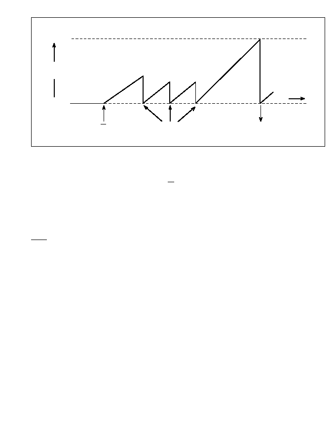
13.3.2 Interval Timer Mode
Interval timer operation begins when the WT/IT bit is cleared to 0 and the TME bit is set to 1.
In the interval timer mode, an IRQ
0
request is generated each time the timer count overflows.
This function can be used to generate IRQ
0
requests at regular intervals. See figure 13-4.
IRQ
0
requests from the watchdog timer module have the same vector as IRQ
0
requests from the
IRQ
0
pin, so the IRQ
0
interrupt-handling routine must check the OVF bit in the TCSR to
determine the source of the interrupt.
TCNT
count
H'00
H'FF
Time t
WT/IT = 1
TIME = 1
H'00 written
to TCNT
OVF = 1
NMI requested
Figure 13-3 Operation in Watchdog Timer Mode
241
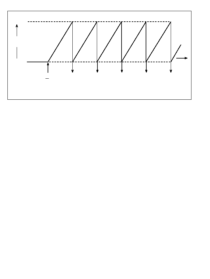
13.3.3 Operation in Software Standby Mode
The watchdog timer has a special function in the software standby mode. Specific watchdog timer
settings are required when the software standby mode is used.
1. Before Transition to the Software Standby Mode: The TME bit must be cleared to 0 to stop
the watchdog timer counter before a transition to the software standby mode. The chip cannot
enter the software standby mode while the TME bit is set to 1. Before entering the software
standby mode, software should also set the clock select bits (CKS2 to CKS0) to a value that
makes the timer overflow interval equal to or greater than the settling time of the clock
oscillator.
2. Recovery from the Software Standby Mode: Recovery from the software standby mode can
be triggered by an NMI request. In this case the recovery proceeds as follows:
When an NMI request signal is received, the clock oscillator starts running and the watchdog
timer starts counting at the rate selected by the clock select bits before the software standby
mode was entered. When the count overflows (H'FF
H'00), the ¯ clock is presumed to be
stable and usable, clock signals are supplied to all modules on the chip, and the NMI interrupt-
handling routine starts executing. This timer overflow does not set the OVF flag, and the TME
bit remains cleared to 0.
TCNT
count
H'00
H'FF
Time t
WT/IT = 0
IRQ
0
IRQ
0
IRQ
0
IRQ
0
IRQ
0
TME = 1
request
request
request
request
request
Figure 13-4 Operation in Interval Timer Mode
242
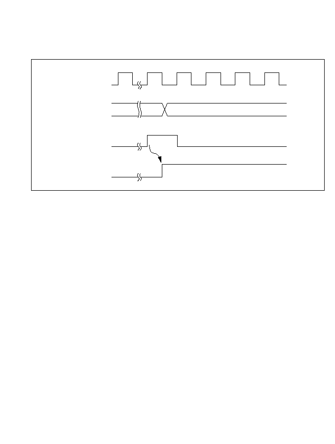
13.3.4 Setting of Overflow Flag
The OVF bit is set to 1 when the timer count overflows. Simultaneously, the WDT module
requests an NMI or IRQ
0
interrupt. The timing is shown in figure 13-5.
13.4 Application Notes
1. Contention between TCNT Write and Increment: If a timer counter clock pulse is
generated during the T
3
state of a write cycle to the timer counter, the write takes priority and
the timer counter is not incremented. See figure 13-6.
TCNT
Internal overflow
signal
OVF
¯
H'FF
H'00
Figure 13-5 Setting of OVF Bit
243
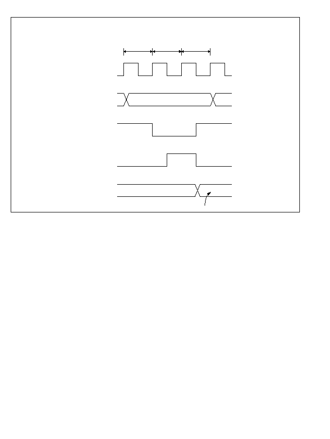
2. Changing the Clock Select Bits (CKS2 to CKS0): Software should stop the watchdog timer
(by clearing the TME bit to 0) before changing the value of the clock select bits. If the clock
select bits are modified while the watchdog timer is running, the timer count may be
incremented incorrectly.
Internal address bus
Internal write signal
TCNT clock pulse
¯
TCNT address
N
M
Write cycle: CPU writes to TCNT
TCNT
Counter write data
T
1
T
2
T
3
Figure 13-6 TCNT Write-Increment Contention
244

Section 14 Serial Communication Interface
14.1 Overview
The H8/532 chip includes a single-channel serial communication interface (SCI) for transferring
serial data to and from other chips. The SCI supports both synchronous and asynchronous data
transfer. Communication control functions are provided by eight internal registers.
14.1.1 Features
The features of the on-chip serial communication interface are:
∑ Selection of asynchronous or synchronous mode
-- Asynchronous mode
The SCI can communicate with a UART (Universal Asynchronous Receiver/Transmitter),
ACIA (Asynchronous Communication Interface Adapter), or other chip that employs
standard asynchronous serial communication. Eight data formats are available.
-- Data length: 7 or 8 bits
-- Stop bit length: 1 or 2 bits
-- Parity: Even, odd, or none
-- Error detection: Parity, overrun, and framing errors
-- Synchronous mode
The SCI can communicate with chips able to synchronize data transfers with clock pulses.
-- Data length: 8 bits
-- Error detection: Overrun errors
∑ Full duplex communication
The transmitting and receiving sections are independent, so the SCI can transmit and receive
simultaneously. Both the transmit and receive sections use double buffering, so continuous data
transfer is possible in either direction.
∑ Built-in baud rate generator
Any specified bit rate can be generated.
∑ Internal or external clock source
The baud rate generator can operate on an internal clock source, or an external clock signal
input at the SCK pin.
∑ Three interrupts
Transmit-end, receive-end, and receive-error interrupts are requested independently. The
transmit-end and receive-end interrupts can be served by the on-chip data transfer controller
(DTC), providing a convenient way to transfer data with minimal CPU programming.
245

14.1.2 Block Diagram
Figure 14-1 shows a block diagram of serial communication interface.
RXD
TXD
SCK
RDR:
RSR:
TDR:
TSR:
SSR:
SCR:
SMR:
BRR:
Receive Data Register
Receive Shift Register
Transmit Data Register
Transmit Shift Register
Serial Status Register
Serial Control Register
Serial Mode Register
Bit Rate Register
RDR
SSR
TDR
SCR
SMR
BRR
Baud-rate
generator
TSR
RSR
Communication
control
Parity generator
Parity check
Clock
External clock
Module data bus
Internal
data bus
Internal clock
source
TXI
RXI
ERI
Interrupt signals
¯
¯/4
¯/16
¯/64
Bus interface
Figure 14-1 Block Diagram of Serial Communication Interface
246

14.1.3 Input and Output Pins
Table 14-1 lists the input and output pins used by the SCI module.
Table 14-1 SCI Input/Output Pins
Name
Abbreviation
I/O
Function
Serial clock
SCK
Input/output
Serial clock input and output.
Receive data
RXD
Input
Receive data input.
Transmit data
TXD
Output
Transmit data output.
14.1.4 Register Configuration
Table 14-2 lists the SCI registers.
Table 14-2 SCI Registers
Name
Abbreviation
R/W
Initial Value
Address
Receive shift register
RSR
--
--
--
Receive data register
RDR
R
H'00
H'FFDD
Transmit shift register
TSR
--
--
--
Transmit data register
TDR
R/W
H'FF
H'FFDB
Serial mode register
SMR
R/W
H'04
H'FFD8
Serial control register
SCR
R/W
H'0C
H'FFDA
Serial status register
SSR
R/(W)
*
H'87
H'FFDC
Bit rate register
BRR
R/W
H'FF
H'FFD9
*
Software can write a "0" to clear the status flag bits, but cannot write a "1."
14.2 Register Descriptions
14.2.1 Receive Shift Register (RSR)
The RSR receives incoming data bits. When one data character has been received, it is transferred
to the receive data register (RDR).
The CPU cannot read or write the RSR directly.
Bit
7
6
5
4
3
2
1
0
Read/Write
--
--
--
--
--
--
--
--
247

14.2.2 Receive Data Register (RDR)--H'FFDD
The RDR stores received data. As each character is received, it is transferred from the RSR to the
RDR, enabling the RSR to receive the next character. This double-buffering allows the SCI to
receive data continuously.
The CPU can read but not write the RDR. The RDR is initialized to H'00 at a reset and in the
standby modes.
14.2.3 Transmit Shift Register (TSR)
The TSR holds the character currently being transmitted. When transmission of this character is
completed, the next character is moved from the transmit data register (TDR) to the TSR and
transmission of that character begins. If the TDR does not contain valid data, the SCI stops
transmitting.
The CPU cannot read or write the TSR directly.
14.2.4 Transmit Data Register (TDR)--H'FFDB
The TDR is an 8-bit readable/writable register that holds the next character to be transmitted.
When the TSR becomes empty, the character written in the TDR is transferred to the TSR.
Continuous data transmission is possible by writing the next byte in the TDR while the current
byte is being transmitted from the TSR.
The TDR is initialized to H'FF at a reset and in the standby modes.
Bit
7
6
5
4
3
2
1
0
Initial value
0
0
0
0
0
0
0
0
Read/Write
R
R
R
R
R
R
R
R
Bit
7
6
5
4
3
2
1
0
Initial value
1
1
1
1
1
1
1
1
Read/Write
R/W
R/W
R/W
R/W
R/W
R/W
R/W
R/W
Bit
7
6
5
4
3
2
1
0
Read/Write
--
--
--
--
--
--
--
--
248

14.2.5 Serial Mode Register (SMR)--H'FFD8
The SMR is an 8-bit readable/writable register that controls the communication format and selects
the clock rate for the internal clock source. It is initialized to H'04 at a reset and in the standby
modes.
Bit 7--Communication Mode (C/A): This bit selects the asynchronous or synchronous
communication mode.
Bit 7
C/A
Description
0
Asynchronous communication.
(Initial value)
1
Communication is synchronized with the serial clock.
Bit 6--Character Length (CHR): This bit selects the character length in asynchronous mode. It
is ignored in synchronous mode.
Bit 6
CHR
Description
0
8 Bits per character.
(Initial value)
1
7 Bits per character.
Bit 5--Parity Enable (PE): This bit selects whether to add a parity bit in asynchronous mode. It
is ignored in synchronous mode.
Bit 5
PE
Description
0
Transmit: No parity bit is added.
(Initial value)
Receive: Parity is not checked.
1
Transmit: A parity bit is added.
Receive: Parity is not checked.
Bit
7
6
5
4
3
2
1
0
C/A
CHR
PE
O/E
STOP
--
CKS1
CKS0
Initial value
0
0
0
0
0
1
0
0
Read/Write
R/W
R/W
R/W
R/W
R/W
--
R/W
R/W
249

Bit 4--Parity Mode (O/E): In asynchronous mode, when parity is enabled (PE = 1), this bit
selects even or odd parity.
Even parity means that a parity bit is added to the data bits for each character to make the total
number of 1's even. Odd parity means that the total number of 1's is made odd.
This bit is ignored when PE = 0 and in the synchronous mode.
Bit 4
O/E
Description
0
Even parity.
(Initial value)
1
Odd parity.
Bit 3--Stop Bit Length (STOP): This bit selects the number of stop bits. It is ignored in the
synchronous mode.
Bit 3
STOP
Description
0
1 Stop bit.
(Initial value)
1
2 Stop bits.
Bit 2--Reserved: This bit cannot be modified and is always read as 1.
Bits 1 and 0--Clock Select 1 and 0 (CKS1 and CKS0): These bits select the internal clock
source when the baud rate generator is clocked from within the H8/532 chip.
Bit 1
Bit 0
CKS1
CKS0
Description
0
0
¯ clock
(Initial value)
0
1
¯/4 clock
1
0
¯/16 clock
1
1
¯/64 clock
250

14.2.6 Serial Control Register (SCR)--H'FFDA
The SCR is an 8-bit readable/writable register that enables or disables various SCI functions. It is
initialized to H'0C at a reset and in the standby modes.
Bit 7--Transmit Interrupt Enable (TIE): This bit enables or disables the transmit-end interrupt
(TXI) requested when the transmit data register empty (TDRE) bit in the serial status register
(SSR) is set to 1.
Bit 7
TIE
Description
0
The transmit-end interrupt request (TXI) is disabled.
(Initial value)
1
The transmit-end interrupt request (TXI) is enabled.
Bit 6--Receive Interrupt Enable (RIE): This bit enables or disables the receive-end interrupt
(RXI) requested when the receive data register full (RDRF) bit in the serial status register (SSR) is
set to 1. It also enables and disables the receive-error interrupt (ERI) request.
Bit 6
RIE
Description
0
The receive-end interrupt (RXI) and receive-error interrupt (ERI)
(Initial value)
requests are disabled.
1
The receive-end interrupt (RXI) and receive-error interrupt (ERI) requests are enabled.
Bit 5--Transmit Enable (TE): This bit enables or disables the transmit function. When the
transmit function is enabled, the TXD pin is automatically used for output. When the transmit
function is disabled, the TXD pin can be used as a general-purpose I/O port.
Bit 5
TE
Description
0
The transmit function is disabled. The TXD pin can be
(Initial value)
used as a general-purpose I/O port.
1
The transmit function is enabled. The TXD pin is used for output.
Bit
7
6
5
4
3
2
1
0
TIE
RIE
TE
RE
--
--
CKE1
CKE0
Initial value
0
0
0
0
1
1
0
0
Read/Write
R/W
R/W
R/W
R/W
--
--
R/W
R/W
251

Bit 4--Receive Enable (RE): This bit enables or disables the receive function. When the receive
function is enabled, the RXD pin is automatically used for input. When the receive function is
disabled, the RXD pin is available as a general-purpose I/O port.
Bit 4
RE
Description
0
The receive function is disabled. The RXD pin can be
(Initial value)
used as a general-purpose I/O port.
1
The receive function is enabled. The RXD pin is used for input.
Bits 3 and 2--Reserved: These bits cannot be modified and are always read as 1.
Bit 1--Clock Enable 1 (CKE1): This bit selects the internal or external clock source for the
baud rate generator. When the external clock source is selected, the SCK pin is automatically
used for input of the external clock signal.
Bit 1
CKE1
Description
0
Internal clock source.
(Initial value)
1
External clock source. (The SCK pin is used for input.)
Bit 0--Clock Enable 0 (CKE0): When an internal clock source is used in synchronous mode,
this bit enables or disables serial clock output at the SCK pin.
This bit is ignored when the external clock is selected, or when the asynchronous mode is
selected.
For further information on the communication format and clock source selection, see tables 14-5
and 14-6 in section 14.3, "Operation."
Bit 0
CKE0
Description
0
The SCK pin is not used by the SCI (and is available as
(Initial value)
a general-purpose I/O port).
1
The SCK pin is used for serial clock output.
252

14.2.7 Serial Status Register (SSR)--H'FFDC
* Software can write a 0 to clear the flags, but cannot write a 1 in these bits.
The SSR is an 8-bit register that indicates transmit and receive status. It is initialized to H'87 at a
reset and in the standby modes.
Bit 7--Transmit Data Register Empty (TDRE): This bit indicates when the TDR contents have
been transferred to the TSR and the next character can safely be written in the TDR.
Bit 7
TDRE
Description
0
This bit is cleared from 1 to 0 when:
1. The CPU reads the TDRE bit, then writes a 0 in this bit.
2. The data transfer controller (DTC) writes data in the TDR.
1
This bit is set to 1 at the following times:
(Initial value)
1. The chip is reset or enters a standby mode.
2. When TDR contents are transferred to the TSR.
3. When TDRE = 0 and the TE bit is cleared to 0.
Bit 6--Receive Data Register Full (RDRF): This bit indicates when one character has been
received and transferred to the RDR.
Bit 6
RDRF
Description
0
This bit is cleared from 1 to 0 when:
(Initial value)
1. The CPU reads the RDRF bit, then writes a 0 in this bit.
2. The data transfer controller (DTC) reads the RDR.
3. The chip is reset or enters a standby mode.
1
This bit is set to 1 when one character is received without error and transferred from the
RSR to the RDR.
Bit
7
6
5
4
3
2
1
0
TDRE
RDRF
ORER
FER
PER
--
--
--
Initial value
1
0
0
0
0
1
1
1
Read/Write
R/(W)
*
R/(W)
*
R/(W)
*
R/(W)
*
R/(W)
*
--
--
--
253

Bit 5--Overrun Error (ORER): This bit indicates an overrun error during reception.
Bit 5
ORER
Description
0
This bit is cleared from 1 to 0 when:
(Initial value)
1. The CPU reads the ORER bit, then writes a 0 in this bit.
2. The chip is reset or enters a standby mode.
1
This bit is set to 1 if reception of the next character ends while the receive data register is
still full (RDRF = 1).
Bit 4--Framing Error (FER): This bit indicates a framing error during data reception in the
synchronous mode. It has no meaning in the asynchronous mode.
Bit 4
FER
Description
0
This bit is cleared to from 1 to 0 when:
(Initial value)
1. The CPU reads the FER bit, then writes a 0 in this bit.
2. The chip is reset or enters a standby mode.
1
This bit is set to 1 if a framing error occurs (stop bit = 0).
Bit 3--Parity Error (PER): This bit indicates a parity error during data reception in the
asynchronous mode, when a communication format with parity bits is used.
This bit has no meaning in the synchronous mode, or when a communication format without
parity bits is used.
Bit 3
PER
Description
0
This bit is cleared from 1 to 0 when:
(Initial value)
1. The CPU reads the PER bit, then writes a 0 in this bit.
2. The chip is reset or enters a standby mode.
1
This bit is set to 1 when a parity error occurs (the parity of the received data does not
match the parity selected by the bit in the SMR).
Bits 2 to 0--Reserved: These bits cannot be modified and are always read as 1.
254

14.2.8 Bit Rate Register (BRR)--H'FFD9
The BRR is an 8-bit register that, together with the CKS1 and CKS0 bits in the SMR, determines
the bit rate output by the baud rate generator.
The BRR is initialized to H'FF (the slowest rate) at a reset and in the standby modes.
Tables 14-3 and 14-4 show examples of BRR (N) and CKS (n) settings for commonly used bit
rates.
Table 14-3 Examples of BRR Settings in Asynchronous Mode (1)
XTAL Frequency (MHz)
2
2.4576
4
4.194304
Bit
Error
Error
Error
Error
Rate
n
N
(%)
n
N
(%)
n
N
(%)
n
N
(%)
110
1
70
+0.03
1
86
+0.31
1
141
+0.03
1
148
≠0.04
150
0
207
+0.16
0
255
0
1
103
+0.16
1
108
+0.21
300
0
103
+0.16
0
127
0
0
207
+0.16
0
217
+0.21
600
0
51
+0.16
0
63
0
0
103
+0.16
0
108
+0.21
1200
0
25
+0.16
0
31
0
0
51
+0.16
0
54
≠0.70
2400
0
12
+0.16
0
15
0
0
25
+0.16
0
26
+1.14
4800
--
--
--
0
7
0
0
12
+0.16
0
13
≠2.48
9600
--
--
--
0
3
0
--
--
--
--
--
--
19200
--
--
--
0
1
0
--
--
--
--
--
--
31250
--
--
--
--
--
--
0
1
0
--
--
--
38400
--
--
--
0
0
0
--
--
--
--
--
--
Bit
7
6
5
4
3
2
1
0
Initial value
1
1
1
1
1
1
1
1
Read/Write
R/W
R/W
R/W
R/W
R/W
R/W
R/W
R/W
255

Table 14-3 Examples of BRR Settings in Asynchronous Mode (2)
XTAL Frequency (MHz)
4.9152
6
7.3728
8
Bit
Error
Error
Error
Error
Rate
n
N
(%)
n
N
(%)
n
N
(%)
n
N
(%)
110
1
174
≠0.26
2
52
+0.50
2
64
+0.70
2
70
+0.03
150
1
127
0
1
155
+0.16
1
191
0
1
207
+0.16
300
0
255
0
1
77
+0.16
1
95
0
1
103
+0.16
600
0
127
0
0
155
+0.16
0
191
0
0
207
+0.16
1200
0
63
0
0
77
+0.16
0
95
0
0
103
+0.16
2400
0
31
0
0
38
+0.16
0
47
0
0
51
+0.16
4800
0
15
0
0
19
≠2.34
0
23
0
0
25
+0.16
9600
0
7
0
--
--
--
0
11
0
0
12
+0.16
19200
0
3
0
--
--
--
0
5
0
--
--
--
31250
--
--
--
0
2
0
--
--
--
0
3
0
38400
0
1
0
--
--
--
0
2
0
--
--
--
Table 14-3 Examples of BRR Settings in Asynchronous Mode (3)
XTAL Frequency (MHz)
9.8304
10
12
12.288
Bit
Error
Error
Error
Error
Rate
n
N
(%)
n
N
(%)
n
N
(%)
n
N
(%)
110
2
86
+0.31
2
88
≠0.25
2
106
≠0.44
2
108
+0.08
150
1
255
0
2
64
+0.16
2
77
0
2
79
0
300
1
127
0
1
129
+0.16
1
155
0
1
159
0
600
0
255
0
1
64
+0.16
1
77
0
1
79
0
1200
0
127
0
0
129
+0.16
0
155
+0.16
0
159
0
2400
0
63
0
0
64
+0.16
0
77
+0.16
0
79
0
4800
0
31
0
0
32
≠1.36
0
38
+0.16
0
39
0
9600
0
15
0
0
15
+1.73
0
19
≠2.34
0
19
0
19200
0
7
0
0
7
+1.73
--
--
--
0
9
0
31250
0
4
≠1.70
0
4
0
0
5
0
0
5
+2.40
38400
0
3
0
0
3
+1.73
--
--
--
0
4
0
256

Table 14-3 Examples of BRR Settings in Asynchronous Mode (4)
XTAL Frequency (MHz)
14.7456
16
19.6608
20
Bit
Error
Error
Error
Error
Rate
n
N
(%)
n
N
(%)
n
N
(%)
n
N
(%)
110
2
130
≠0.07
2
141
+0.03
2
174
≠0.26
3
43
+0.88
150
2
95
0
2
103
+0.16
2
127
0
2
129
+0.16
300
1
191
0
1
207
+0.16
1
255
0
2
64
+0.16
600
1
95
0
1
103
+0.16
1
127
0
1
129
+0.16
1200
0
191
0
0
207
+0.16
0
255
0
1
64
+0.16
2400
0
95
0
0
103
+0.16
0
127
0
0
129
+0.16
4800
0
47
0
0
51
+0.16
0
63
0
0
64
+0.16
9600
0
23
0
0
25
+0.16
0
31
0
0
32
≠1.36
19200
0
11
0
0
12
+0.16
0
15
0
0
15
+1.73
31250
--
--
--
0
7
0
0
9
≠1.70
0
9
0
38400
0
5
0
--
--
--
0
7
0
0
7
+1.73
B = OSC
◊
106/[64
◊
22n
◊
(N + 1)]
B :
Bit rate
N :
BRR value (0
N
255)
OSC :
Crystal oscillator frequency in MHz
n :
Internal clock source (0, 1, 2, or 3)
The meaning of n is given by the table below:
n
CKS1
CKS0
Clock
0
0
0
¯
1
0
1
¯/4
2
1
0
¯/16
3
1
1
¯/64
257

Table 14-4 Examples of BRR Settings in Synchronous Mode
XTAL Frequency (MHz)
Bit
2
4
8
10
16
20
Rate
n
N
n
N
n
N
n
N
n
N
n
N
100
--
--
--
--
--
--
--
--
--
--
--
--
250
1
249
2
124
2
249
--
--
3
124
--
--
500
1
124
1
249
2
124
--
--
2
249
--
--
1K
0
249
1
124
1
249
--
--
2
124
--
--
2.5M
0
99
0
199
1
99
1
124
1
199
1
249
5K
0
49
0
99
0
199
0
249
1
99
1
124
10K
0
24
0
49
0
99
0
124
0
199
0
249
25K
0
9
0
19
0
39
0
49
0
79
0
99
50K
0
4
0
9
0
19
0
24
0
39
0
49
100K
--
--
0
4
0
9
--
--
0
19
0
24
250K
0
0
0
1
0
3
0
4
0
7
0
9
500K
0
0
0
1
--
--
0
3
0
4
1M
0
0
--
--
0
1
--
--
2.5M
0
0
Notes:
Blank: No setting is available.
--: A setting is available, but the bit rate is inaccurate.
B = OSC/[8
◊
2
2n
◊
(N + 1)]
B :
Bit rate
N :
BRR value (0
N
255)
OSC :
Crystal oscillator frequency in MHz
n :
Internal clock source (0, 1, 2, or 3)
The meaning of n is given by the table below:
n
CKS1
CKS0
Clock
0
0
0
¯
1
0
1
¯/4
2
1
0
¯/16
3
1
1
¯/64
258

14.3 Operation
14.3.1 Overview
The SCI supports serial data transfer in both asynchronous and synchronous modes.
The communication format depends on settings in the SMR as indicated in table 14-5. The clock
source and usage of the SCK pin depend on settings in the SMR and SCR as indicated in table 14-6.
Table 14-5 Communication Formats Used by SCI
SMR
Stop Bit
C/A
CHR
PE
STOP
Mode
Format
Parity
Length
0
0
0
0
Asynchronous
8-Bit data
None
1
1
2
1
0
Yes
1
1
2
1
0
0
7-Bit data
None
1
1
2
1
0
Yes
1
1
2
1
--
--
--
Synchronous
8-Bit data
--
--
Table 14-6 SCI Clock Source Selection
SMR
SCR
Clock
C/A
CKE1
CKE0
Source
SCK Pin
0
0
0
Internal
I/O port
*
(Async
1
Clock output at same frequency as baud rate
mode)
1
0
External
Clock input at 16 times the baud rate frequency
1
1
0
0
Internal
Serial clock output
(Sync
1
mode)
1
0
External
Serial clock input
1
*
Cannot be used by the SCI.
Transmitting and receiving operations in the two modes are described next.
259
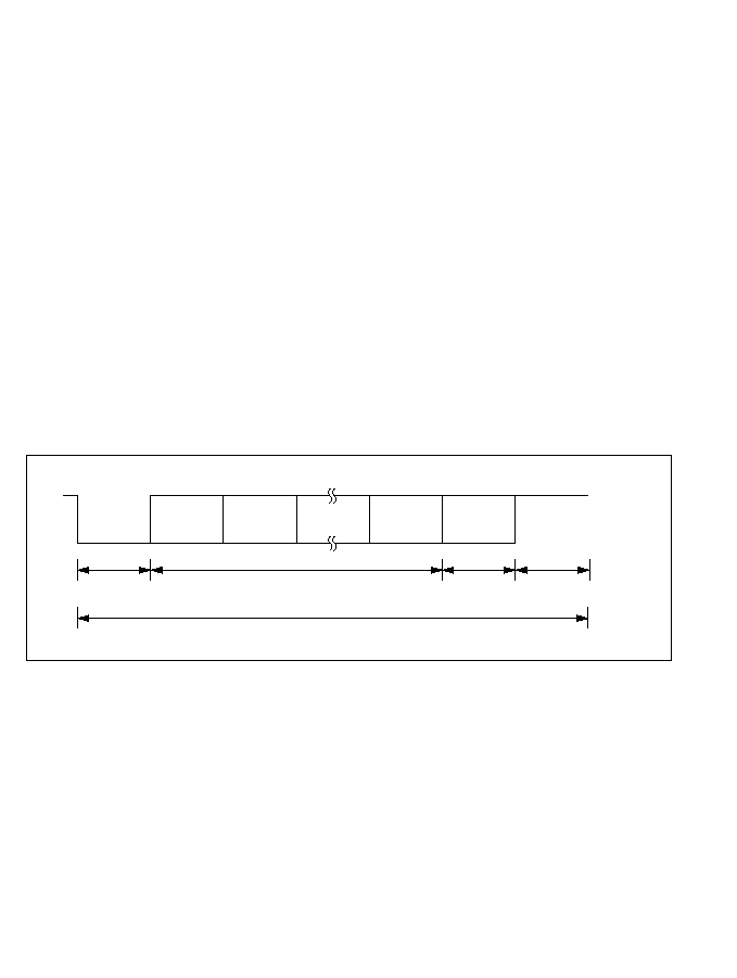
14.3.2 Asynchronous Mode
In asynchronous mode, each character is individually synchronized by framing it with a start bit
and stop bit.
Full duplex data transfer is possible because the SCI has independent transmit and receive
sections. Double buffering in both sections enables the SCI to be programmed for continuous data
transfer.
Figure 14-2 shows the general format of one character sent or received in the asynchronous mode.
The communication channel is normally held in the mark state (High). Character transmission or
reception starts with a transition to the space state (Low).
The first bit transmitted or received is the start bit (Low). It is followed by the data bits, in which
the least significant bit (LSB) comes first. The data bits are followed by the parity bit, if present,
then the stop bit or bits (High) confirming the end of the frame.
In receiving, the SCI synchronizes on the falling edge of the start bit, and samples each bit at the
center of bit (at the 8th cycle of the internal serial clock, which runs at 16 times the bit rate).
1. Data Format: Table 14-7 lists the data formats that can be sent and received in asynchronous
mode. Eight formats can be selected by bits in the SMR.
Figure 14-2 Data Format in Asynchronous Mode
Start bit
D0
D1
Dn
Parity bit
Stop bit
Idle state
One character
1 bit
7 or 8 bits
0 or 1 bit
1 or 2 bits
260
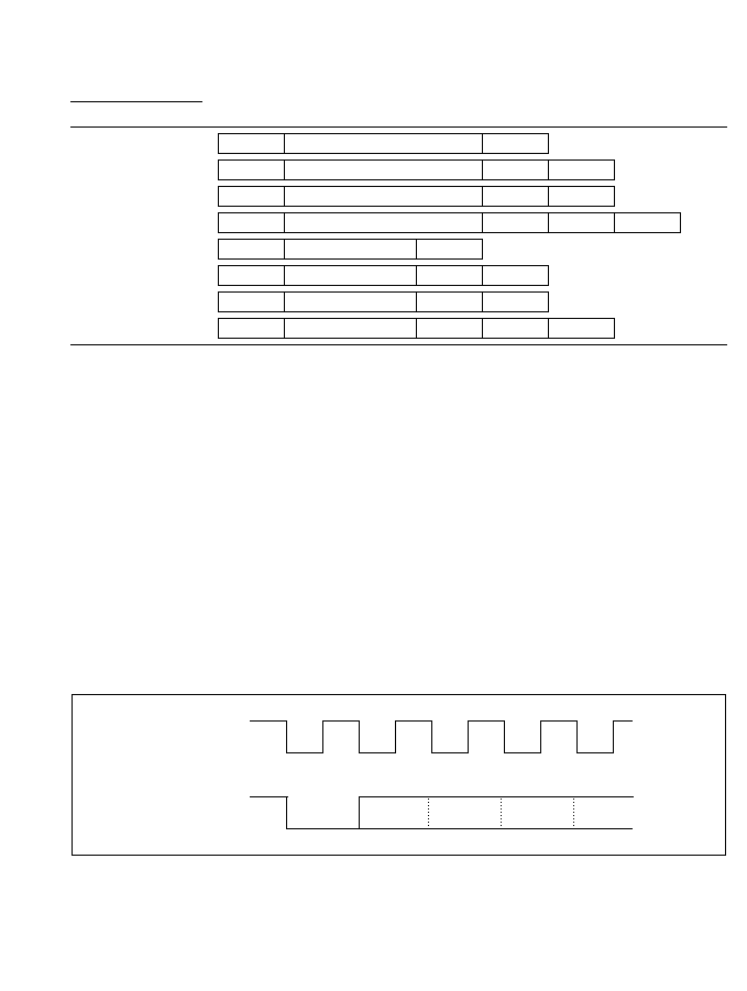
Table 14-7 Data Formats in Asynchronous Mode
SMR Bits
CHR
PE
STOP
Data Format
0
0
0
START
8-Bit data
STOP
0
0
1
START
8-Bit data
STOP
STOP
0
1
0
START
8-Bit data
P
STOP
0
1
1
START
8-Bit data
P
STOP
STOP
1
0
0
START
7-Bit data
STOP
1
0
1
START
7-Bit data
STOP
STOP
1
1
0
START
7-Bit data
P
STOP
1
1
1
START
7-Bit data
P
STOP
STOP
Note:
START: Start bit
STOP: Stop bit
P: Parity bit
2. Clock: In the asynchronous mode it is possible to select either an internal clock created by the
on-chip baud rate generator, or an external clock input at the SCK pin. Refer to table 14-6.
If an external clock is input at the SCK pin, its frequency should be 16 times the desired baud
rate.
If the internal clock provided by the on-chip baud rate generator is selected and the SCK pin is
used for clock output, the output clock frequency is equal to the baud rate, and the clock pulse
rises at the center of the transmit data bits. Figure 14-3 shows the phase relationship between
the output clock and transmit data.
Output clock
Transmit data
Start bit
D0
D1
D2
Figure 14-3 Phase Relationship between Clock Output and Transmit Data
261

3. Data Transmission and Reception
∑ SCI Initialization: Before data can be transmitted or received, the SCI must be initialized
by software. To initialize the SCI, software must clear the TE and RE bits to 0, then execute
the following procedure.
(1) Set the desired communication format in the SMR.
(2) Write the value corresponding to the desired bit rate in the BRR. (This step is not
necessary if an external clock is used.)
(3) Select the clock and enable desired interrupts in the SCR.
(4) Set the TE and/or RE bit in the SCR to 1.
The TE and RE bits must both be cleared to 0 whenever the operating mode or data format is
changed.
After changing the operating mode or data format, before setting the TE and RE bits to 1
software must wait for at least the transfer time for 1 bit at the selected baud rate, to make sure
the SCI is initialized. If an external clock is used, the clock must not be stopped.
When clearing the TDRE bit during data transmission, to assure transfer of the correct data, do
not clear the TDRE bit until after writing data in the TDR. Similarly, in receiving data, do not
clear the RDRF bit until after reading data from the RDR.
∑ Data Transmission: The procedure for transmitting data is as follows.
(1) Set up the desired transmitting conditions in the SMR, SCR, and BRR.
(2) Set the TE bit in the SCR to 1.
The TXD pin will automatically be switched to output and one frame* of all 1's will be
transmitted, after which the SCI is ready to transmit data.
(3) Check that the TDRE bit is set to 1, then write the first byte of transmit data in the TDR.
Next clear the TDRE bit to 0.
* A frame is the data for one character, including the start bit and stop bit(s).
262

(4) The first byte of transmit data is transferred from the TDR to the TSR and sent in the
designated format as follows.
i)
Start bit (one 0 bit)
ii)
Transmit data (seven or eight bits, starting from bit 0)
iii) Parity bit (odd or even parity bit, or no parity bit)
iv) Stop bit (one or two consecutive 1 bits)
(5) Transfer of the transmit data from the TDR to the TSR makes the TDR empty, so the
TDRE bit is set to 1.
If the TIE bit is set to 1, a transmit-end interrupt (TXI) is requested.
When the transmit function is enabled but the TDR is empty (TDRE = 1), the output at the
TXD pin is held at 1 until the TDRE bit is cleared to 0.
∑ Data Reception: The procedure for receiving data is as follows.
(1) Set up the desired receiving conditions in the SMR, SCR, and BRR.
(2) Set the RE bit in the SCR to 1.
The RXD pin will automatically be switched to input and the SCI is ready to receive data.
(3) The SCI synchronizes with the incoming data by detecting the start bit, and places the
received bits in the RSR. At the end of the data, the SCI checks that the stop bit is 1.
If the stop bit length is 2 bits, in ZTAT versions the SCI checks that both bits are 1, but in
masked-ROM versions, only the first bit is checked.
(4) When a complete frame has been received, the SCI transfers the received data to the RDR
so that it can be read. If the character length is 7 bits, the most significant bit of the RDR
is cleared to 0. At the same time, the SCI sets the RDRF bit in the SSR to 1. If the RIE bit
is set to 1, a receive-end interrupt (RXI) is requested.
(5) The RDRF bit is cleared to 0 when the CPU reads the SSR, then writes a 0 in the RDRF
bit, or when the RDR is read by the data transfer controller (DTC). The RDR is then ready
to receive the next character from the RSR.
When a frame is not received correctly, a receive error occurs. There are three types of receive
errors, listed in table 14-8.
If a receive error occurs, the RDRF bit in the SSR is not set to 1. The corresponding error flag
is set to 1 instead. If the RIE bit in the SCR is set to 1, a receive-error interrupt (ERI) is
requested.
263

When a framing or parity error occurs, the RSR contents are transferred to the RDR. If an
overrun error occurs, however, the RSR contents are not transferred to the RDR.
If multiple receive errors occur simultaneously, all the corresponding error flags are set to 1.
To clear a receive-error flag (ORER, FER, or PER), software must read the SSR, then write a 0
in the flag bit.
Table 14-8 Receive Errors
Name
Abbreviation
Description
Overrun error
ORER
Reception of the next frame ends while the RDRF bit is still
set to 1.
The RSR contents are not transferred to the RDR.
Framing error
FER
A stop bit is 0.
The RSR contents are transferred to the RDR.
Parity error
PER
The parity of a frame does not match the value selected by the bit
in the SMR.
The RSR contents are transferred to the RDR.
14.3.3 Synchronous Mode
The synchronous mode is suited for high-speed, continuous data transfer. Each bit of data is
synchronized with a serial clock pulse.
Continuous data transfer is enabled by the double buffering employed in both the transmit and
receive sections of the SCI. Full duplex communication is possible because the transmit and
receive sections are independent.
1. Data Format: Figure 14-4 shows the communication format used in the synchronous mode.
The data length is 8 bits for both the transmit and receive directions. The least significant bit
(LSB) is sent and received first. Each bit of transmit data is output from the falling edge of the
serial clock pulse to the next falling edge. Received bits are latched on the rising edge of the
serial clock pulse.
264
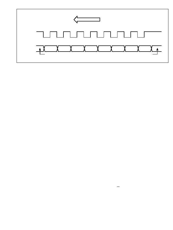
2. Clock: Either the internal serial clock created by the on-chip baud rate generator or an external
clock input at the SCK pin can be selected in the synchronous mode. See table 14-6 for details.
3. Data Transmission and Reception
∑ SCI Initialization: Before data can be transmitted or received, the SCI must be initialized
by software. To initialize the SCI, software must clear the TE and RE bits to 0 to disable
both the transmit and receive functions, then execute the following procedure.
(1) Write the value corresponding to the desired bit rate in the BRR. (This step is not
necessary if an external clock is used.)
(2) Select the clock in the SCR.
(3) Select the synchronous mode in the SMR*.
(4) Set the TE and/or RE bit to 1, and enable desired interrupts in the SCR.
The TE and RE bits must both be cleared to 0 whenever the operating mode or data format is
changed. After changing the operating mode or data format, before setting the TE and RE bits
to 1 software must wait for at least 1 bit transfer time at the selected communication speed, to
make sure the SCI is initialized.
* The SCK pin is used for input or output according to the C/A bit in the serial mode register
(SMR) and the CKE0 and CKE1 bits in the serial control register (SCR). (See table 14-6.)
To prevent unwanted output at the SCK pin, pay attention to the order in which you set SMR
and SCR.
Don't-care
Don't-care
Data
Serial clock
Bit 0
Bit 1
Bit 2
Bit 3
Bit 4
Bit 5
Bit 6
Bit 7
Transmission direction
Figure 14-4 Data Format in Synchronous Mode
265

When clearing the TDRE bit during data transmission, to assure correct data transfer, do not
clear the TDRE bit until after writing data in the TDR. Similarly, in receiving data, do not
clear the RDRF bit until after reading data from the RDR.
∑ Data Transmission: The procedure for transmitting data is as follows.
(1) Set up the desired transmitting conditions in the SMR, BRR, and SCR.
(2) Set the TE bit in the SCR to 1.
The TXD pin will automatically be switched to output, after which the SCI is ready to
transmit data.
(3) Check that the TDRE bit is set to 1, then write the first byte of transmit data in the TDR.
Next clear the TDRE bit to 0.
(4) The first byte of transmit data is transferred from the TDR to the TSR and sent, each bit
synchronized with a clock pulse. Bit 0 is sent first.
Transfer of the transmit data from the TDR to the TSR makes the TDR empty, so the
TDRE bit is set to 1. If the TIE bit is set to 1, a transmit-end interrupt (TXI) is
requested.
The TDR and TSR function as a double buffer. Continuous data transmission can be achieved
by writing the next transmit data in the TDR and clearing the TDRE bit to 0 while the SCI is
transmitting the current data from the TSR.
If an internal clock source is selected, after transferring the transmit data from the TDR to the
TSR, while transmitting the data from the TSR the SCI also outputs a serial clock signal at the
SCK pin. When all data bits in the TSR have been transmitted, if the TDR is empty (TDRE =
1), serial clock output is suspended until the next data byte is written in the TDR and the TDRE
bit is cleared to 0. During this interval the TXD pin is held at the value of the last bit
transmitted.
If the external clock source is selected, data transmission is synchronized with the clock signal
input at the SCK pin. When all data bits in the TSR have been transmitted, if the TDR is
empty (TDRE = 1) but external clock pulses continue to arrive, the TXD pin outputs a string of
bits equal to the last bit transmitted.
∑ Data Reception: The procedure for receiving data is as follows.
(1) Set up the desired receiving conditions in the SMR, BRR, and SCR.
266

(2) Set the RE bit in the SCR to 1.
The RXD pin will automatically be switched to input and the SCI is ready to receive
data.
(3) Incoming data bits are latched in the RSR on eight clock pulses.
When 8 bits of data have been received, the SCI sets the RDRF bit in the SSR to 1. If
the RIE bit is set to 1, a receive-end interrupt (RXI) is requested.
(4) The SCI transfers the received data byte to the RDR so that it can be read.
The RDRF bit is cleared when the program reads the RDRF bit in the SSR, then writes a
0 in the RDRF bit, or when the data transfer controller (DTC) reads the RDR.
The RDR and RSR function as a double buffer. Data can be received continuously by reading
each byte of data from the RDR and clearing the RDRF bit to 0 before the last bit of the next
byte is received.
In general, an external clock source should be used for receiving data.
If an internal clock source is selected, the SCI starts receiving data as soon as the RE bit is set
to 1. The serial clock is also output at the SCK pin. The SCI continues receiving until the RE
bit is cleared to 0.
If the last bit of the next data byte is received while the RDRF bit is still set to 1, an overrun
error occurs and the ORER bit is set to 1. If the RIE bit is set to 1, a receive-error interrupt
(ERI) is requested. The data received in the RSR are not transferred to the RDR when an
overrun error occurs.
After an overrun error, reception of the next data is enabled when the ORER bit is cleared to 0.
∑ Simultaneous Transmit and Receive: The procedure for transmitting and receiving
simultaneously is as follows:
(1) Set up the desired communication conditions in the SMR, BRR, and SCR.
(2) Set the TE and RE bits in the SCR to 1.
The TXD and RXD pins are automatically switched to output and input, respectively,
and the SCI is ready to transmit and receive data.
(3) Data transmitting and receiving start when the TDRE bit in the SSR is cleared to 0.
(4) Data are sent and received in synchronization with eight clock pulses.
267

(5) First, the transmit data are transferred from the TDR to the TSR. This makes the TDR
empty, so the TDRE bit is set to 1. If the TIE bit is set to 1, a transmit-end interrupt
(TXI) is requested.
If continuous data transmission is desired, the CPU must read the TDRE bit in the SSR,
write the next transmit data in the TDR, then clear the TDRE bit to 0. Alternatively, the
DTC can write the next transmit data in the TDR, in which case the TDRE bit is cleared
automatically.
If the TDRE bit is not cleared to 0 by the time the SCI finishes sending the current byte
from the TSR, the TXD pin continues to output the last bit in the TSR.
(6) In the receiving section, when 8 bits of data have been received they are transferred from
the RSR to the RDR and the RDRF bit in the SSR is set to 1. If the RIE bit is set to 1, a
receive-end interrupt (RXI) is requested.
(7) To clear the RDRF bit software read the RDRF bit in the SSR, read the data in the RDR,
then write a 0 in the RDRF bit. Alternatively, the DTC can read the RDR, in which case
the RDRF bit is cleared automatically.
For continuous data reception, the RDRF bit must be cleared to 0 before the last bit of
the next byte of data is received.
If the last bit of the next byte is received while the RDRF bit is still set to 1, an overrun error
occurs. The error is handled as described under "Data Reception" above. The overrun error
does not affect the transmit section of the SCI, which continues to transmit normally.
14.4 CPU Interrupts and DTC Interrupts
The SCI can request three types of interrupts: transmit-end (TXI), receive-end (RXI), and
receive-error (ERI). Interrupt requests are enabled or disabled by the TIE and RIE bits in the
SCR. Independent signals are sent to the interrupt controller for each type of interrupt. The
transmit-end and receive-end interrupt request signals are obtained from the TDRE and RDRF
flags. The receive-error interrupt request signal is the logical OR of the three error flags: overrun
error (ORER), framing error (FER), and parity error (PER). Table 14-9 lists information about
these interrupts.
268

Table 14-9 SCI Interrupts
DTC Service
Interrupt
Description
Available?
Priority
ERI
Receive-error interrupt, requested when
No
High
ORER, FER, or PER is set.
RXI
Receive-end interrupt, requested when
Yes
RDRF is set.
TXI
Transmit-end interrupt, requested when
Yes
TDRE is set.
Low
The TXI and RXI interrupts can be served by the data transfer controller (DTC) to have a data
transfer performed. When the DTC serves one of these interrupts, it clears the TDRE or RDRF bit
to 0 under the following conditions, which differ between the two bits.
When invoked by a TXI request, if the DTC writes to the TDR, it automatically clears the TDRE
bit to 0. When invoked by an RXI request, if the DTC reads from the RDR, it automatically clears
the RDRF bit to 0.
See section 6, "Data Transfer Controller" for further information on the DTC.
14.5 Application Notes
Application programmers should note the following features of the SCI.
1. TDR Write: The TDRE bit in the SSR is simply a flag that indicates that the TDR contents
have been transferred to the TSR. The TDR contents can be rewritten regardless of the TDRE
value. If a new byte is written in the TDR while the TDRE bit is 0, before the old TDR
contents have been moved into the TSR, the old byte will be lost. Normally, software should
check that the TDRE bit is set to 1 before writing to the TDR.
2. Multiple Receive Errors: Table 14-10 lists the values of flag bits in the SSR when multiple
receive errors occur, and indicates whether the RSR contents are transferred to the RDR.
269

Table 14-10 SSR Bit States and Data Transfer When Multiple Receive Errors Occur
SSR Bits
Receive Error
RDRF
ORER
FER
PER
RSR to RDR
*
2
Overrun error
1
*
1
1
0
0
No
Framing error
0
0
1
0
Yes
Parity error
0
0
0
1
Yes
Overrun + framing errors
1
*
1
1
1
0
No
Overrun + parity errors
1
*
1
1
0
1
No
Framing + parity errors
0
0
1
1
Yes
Overrun + framing + parity errors
1
*
1
1
1
1
No
*
1 Set to 1 before the overrun error occurs.
*
2 Yes: The RSR contents are transferred to the RDR.
No:
The RSR contents are not transferred to the RDR.
3. Line Break Detection: When the RXD pin receives a continuous stream of 0's in the
asynchronous mode (line-break state), a framing error occurs because the SCI detects a 0 stop
bit. The value H'00 is transferred from the RSR to the RDR. Software can detect the line-
break state as a framing error accompanied by H'00 data in the RDR.
The SCI continues to receive data, so if the FER bit is cleared to 0 another framing error will
occur.
4. Sampling Timing and Receive Margin in Asynchronous Mode: The serial clock used by
the SCI in asynchronous mode runs at 16 times the bit rate. The falling edge of the start bit is
detected by sampling the RXD input on the falling edge of this clock. After the start bit is
detected, each bit of receive data in the frame (including the start bit, parity bit, and stop bit or
bits) is sampled on the rising edge of the serial clock pulse at the center of the bit.
See figure 14-5.
It follows that the receive margin can be calculated as in equation (1).
When the absolute frequency deviation of the clock signal is 0 and the clock duty factor is 0.5,
data can theoretically be received with distortion up to the margin given by equation (2). This
is a theoretical limit, however. In practice, system designers should allow a margin of 20% to
30%.
270

M = {(0.5 ≠ 1/2N) ≠ (D ≠ 0.5)/N ≠ (L ≠ 0.5)F}
◊
100 [%]
(1)
N:
Receive margin
N:
Ratio of basic clock to bit rate (16)
D:
Duty factor of clock--ratio of High pulse width to Low width (0.5 to 1.0)
L:
Frame length (9 to 12)
F:
Absolute clock frequency deviation
When D = 0.5 and F= 0
M = (0.5 ≠1/2
◊
16)
◊
100 [%] = 46.875%
(2)
Basic clock
Receive data
Start bit
Sync sampling
Data sampling
≠7.5 pulses
+7.5 pulses
D0
D1
0 1 2 3 4 5 6 7 8 9 10 11 12 13 14 15 16 1 2 3 4 5 6 7 8 9 10 11 12 13 14 15 16 1 2 3 4 5
Figure 14-5 Sampling Timing (Asynchronous Mode)
271

Section 15 A/D Converter
15.1 Overview
The H8/532 chip includes an analog-to-digital converter module which can be programmed for
input of analog signal on up to eight channels. A/D conversion is performed by the successive
approximations method with 10-bit resolution.
15.1.1 Features
The features of the on-chip A/D module are:
∑ Eight analog input channels
∑ Sample and hold circuit
∑ 10-Bit resolution
∑ Rapid conversion
Conversion time is 13.8µs per channel (at ¯ = 10MHz)
∑ Single and scan modes
-- Single mode: A/D conversion is performed once.
-- Scan mode: A/D conversion is performed in a repeated cycle on one to four channels.
∑ Four 16-bit data registers
These registers store A/D conversion results for up to four channels.
∑ A CPU interrupt (ADI) can be requested at the completion of each A/D conversion cycle.
This interrupt can also be served by the on-chip data transfer controller (DTC), providing a
convenient way to move results into memory.
273

15.1.2 Block Diagram
Figure 15-1 shows a block diagram of A/D converter.
AV
CC
AV
SS
AN
0
AN
1
AN
2
AN
3
AN
4
AN
5
AN
6
AN
7
Analog multiplexer
Sample & hold
circuit
+
≠
10-Bit D/A
Module data bus
Internal
data bus
Control circuit
¯/8
¯/16
ADI
Interrupt signal
ADDRA:
ADDRB:
ADDRC:
ADDRD:
ADCSR:
A/D Data Register A
A/D Data Register B
A/D Data Register C
A/D Data Register D
A/D Control/Status Register
Successive approximations
register
ADDRA
ADDRB
ADDRC
ADDRD
ADCSR
Bus interface
Figure 15-1 Block Diagram of A/D Converter
274

15.1.3 Input Pins
Table 15-1 lists the input pins used by the A/D converter module.
The eight analog input pins are divided into two groups, consisting of analog inputs 0 to 3 (AN
0
to
AN
3
) and analog inputs 4 to 7 (AN
4
to AN
7
), respectively.
Table 15-1 A/D Input Pins
Name
Abbreviation
I/O
Function
Analog supply
AV
CC
Input
Power supply and reference voltage for the
voltage
analog circuits.
Analog ground
AV
SS
Input
Ground and reference voltage for the analog circuits.
Analog input 0
AN
0
Input
Analog input pins, group 0
Analog input 1
AN
1
Input
Analog input 2
AN
2
Input
Analog input 3
AN
3
Input
Analog input 4
AN
4
Input
Analog input pins, group 1
Analog input 5
AN
5
Input
Analog input 6
AN
6
Input
Analog input 7
AN
7
Input
15.1.4 Register Configuration
Table 15-2 lists the registers of the A/D converter module.
Table 15-2 A/D Registers
Name
Abbreviation
R/W
Initial Value
Address
A/D data register A (High)
ADDRA (H)
R
H'00
H'FFE0
A/D data register A (Low)
ADDRA (L)
R
H'00
H'FFE1
A/D data register B (High)
ADDRB (H)
R
H'00
H'FFE2
A/D data register B (Low)
ADDRB (L)
R
H'00
H'FFE3
A/D data register C (High)
ADDRC (H)
R
H'00
H'FFE4
A/D data register C (Low)
ADDRC (L)
R
H'00
H'FFE5
A/D data register D (High)
ADDRD (H)
R
H'00
H'FFE6
A/D data register D (Low)
ADDRD (L)
R
H'00
H'FFE7
A/D control/status register
ADCSR
R/(W)
*
H'00
H'FFE8
*
Software can write "0" to clear the status flag bits but cannot write 1.
275

15.2 Register Descriptions
15.2.1 A/D Data Registers (ADDR)--H'FFE0 to H'FFE7
The four A/D data registers (ADDRA to ADDRD) are 16-bit read-only registers that store the
results of A/D conversion.
Each result consist of 10 bits. The first 8 bits are stored in the upper byte of the data register
corresponding to the selected channel. The last two bits are stored in the lower data register byte.
Each data register is assigned to two analog input channels as indicated in table 15-3.
The A/D data registers are always readable by the CPU. The upper byte can be read directly. The
lower byte is read via a temporary register. See section 15-3, "CPU Interface" for details.
The unused bits (bits 5 to 0) of the lower data register byte are always read as 0.
The A/D data registers are initialized to H'0000 at a reset and in the standby modes.
Table 15-3 Assignment of Data Registers to Analog Input Channels
Analog Input Channel
Group 0
Group 1
A/D Data Register
AN
0
AN
4
ADDRA
AN
1
AN
5
ADDRB
AN
2
AN
6
ADDRC
AN
3
AN
7
ADDRD
Bit
7
6
5
4
3
2
1
0
ADDRn H
AD
9
AD
8
AD
7
AD
6
AD
5
AD
4
AD
3
AD
2
Initial value
0
0
0
0
0
0
0
0
Read/Write
R
R
R
R
R
R
R
R
(n = A to D)
Bit
7
6
5
4
3
2
1
0
ADDRn H
AD
1
AD
0
--
--
--
--
--
--
Initial value
0
0
0
0
0
0
0
0
Read/Write
R
R
R
R
R
R
R
R
(n = A to D)
276

15.2.2 A/D Control/Status Register (ADCSR)--H'FFE8
* Software can write a 0 in bit 7 to clear the flag, but cannot write a 1 in this bit.
The A/D control/status register (ADCSR) is an 8-bit readable/writable register that controls the
operation of the A/D converter module.
The ADCSR is initialized to H'00 at a reset and in the standby modes.
Bit 7--A/D End Flag (ADF): This status flag indicates the end of one cycle of A/D conversion.
Bit 7
ADF
Description
0
This bit is cleared from 1 to 0 when:
(Initial value)
1. The chip is reset or placed in a standby mode.
2. The CPU reads the ADF bit, then writes a "0" in this bit.
3. An A/D interrupt is served by the data transfer controller (DTC).
1
This bit is set to 1 at the following times:
1. Single mode: when one A/D conversion is completed.
2. Scan mode: when inputs on all selected channels have been converted.
Bit 6--A/D Interrupt Enable (ADIE): This bit selects whether to request an A/D interrupt
(ADI) when A/D conversion is completed.
Bit 6
ADIE
Description
0
The A/D interrupt request (ADI) is disabled.
(Initial value)
1
The A/D interrupt request (ADI) is enabled.
Bit
7
6
5
4
3
2
1
0
ADF
ADIE
ADST
SCAN
CKS
CH2
CH1
CH0
Initial value
0
0
0
0
0
0
0
0
Read/Write
R/(W)
*
R/W
R/W
R/W
R/W
R/W
R/W
R/W
277

Bit 5--A/D Start (ADST): The A/D converter operates while this bit is set to 1. In the single
mode, this bit is automatically cleared to 0 at the end of each A/D conversion.
Bit 5
ADST
Description
0
A/D conversion is halted.
(Initial value)
1
1. Single mode: One A/D conversion is performed. The ADST bit is automatically
cleared to 0 at the end of the conversion.
2. Scan mode: A/D conversion starts and continues cyclically on the selected channels
until the ADST bit is cleared to 0.
Bit 4--Scan Mode (SCAN): This bit selects the scan mode or single mode of operation.
See section 15.4, "Operation" for descriptions of these modes.
The mode should be changed only when the ADST bit is cleared to 0.
Bit 4
SCAN
Description
0
Single mode
(Initial value)
1
Scan mode
Bit 3--Clock Select (CKS): This bit controls the A/D conversion time.
The conversion time should be changed only when the ADST bit is cleared to 0.
Bit 3
CKS
Description
0
Conversion time = 274 states
(Initial value)
1
Conversion time = 138 states
Bits 2 to 0--Channel Select 2 to 0 (CH2 to CH0): These bits and the SCAN bit combine to
select one or more analog input channels.
The channel selection should be changed only when the ADST bit is cleared to 0.
278

Group Select
Channel Select
Selected Channels
CH2
CH1
CH0
Single Mode
Scan Mode
0
0
0
AN
0
AN
0
0
1
AN
1
AN
0
and AN
1
1
0
AN
2
AN
0
to AN
2
1
1
AN
3
AN
0
to AN
3
1
0
0
AN
4
AN
4
0
1
AN
5
AN
4
and AN
5
1
0
AN
6
AN
4
to AN
6
1
1
AN
7
AN
4
to AN
7
15.3 CPU Interface
The A/D data registers (ADDRA to ADDRD) are 16-bit registers. The upper byte of each register
can be read directly, but the lower byte is accessed through an 8-bit temporary register (TEMP).
When the CPU or DTC reads the upper byte of an A/D data register, at the same time as the upper
byte is placed on the internal data bus, the lower byte is transferred to TEMP. When the lower
byte is accessed, the value in TEMP is placed on the internal data bus.
A program that requires all 10 bits of an A/D result should perform word access, or should read
first the upper byte, then the lower byte of the A/D data register. Either way, it is assured of
obtaining consistent data. Consistent data are not assured if the program reads the lower byte first.
A program that requires only 8-bit A/D accuracy should perform byte access to the upper byte of
the A/D data register. The value in TEMP can be left unread.
Figure 15-2 shows the data flow when the CPU (or DTC) reads an A/D data register.
279

15.4 Operation
The A/D converter performs 10 successive approximations to obtain a result ranging from H'0000
(corresponding to AV
SS
) to H'FFC0 (corresponding to AV
CC
). Only the first 10 bits of the result
are significant.
The A/D converter module can be programmed to operate in single mode or scan mode as
explained below.
< Lower byte read >
CPU
receives
data H'40
Bus interface
Module data bus
< Upper byte read >
CPU
receives
data H'AA
Bus interface
TEMP
[H'40]
ADDRn H
[H'AA]
ADDRn L
[H'40]
Module data bus
(n = A to D)
TEMP
[H'40]
ADDRn H
[H'AA]
ADDRn L
[H'40]
(n = A to D)
Figure 15-2 Read Access to A/D Data Register (When Register Contains H'AA40)
280

15.4.1 Single Mode
The single mode is suitable for obtaining a single data value from a single channel. A/D
conversion starts when the ADST bit is set to 1. During the conversion process the ADST bit
remains set to 1. When conversion is completed, the ADST bit is automatically cleared to 0.
When the conversion is completed, the ADF bit is set to 1. If the interrupt enable bit (ADIE) is
also set to 1, an A/D conversion end interrupt (ADI) is requested, so that the converted data can be
processed by an interrupt-handling routine. Alternatively, the interrupt can be served by the data
transfer controller (DTC).
When an A/D interrupt is served by the DTC, the DTC automatically clears the ADF bit to 0.
When an A/D interrupt is served by the CPU, however, the ADF bit remains set until the CPU
reads the ADCSR, then writes a 0 in the ADF bit.
Before selecting the single mode, clock, and analog input channel, software should clear the
ADST bit to 0 to make sure the A/D converter is stopped. Changing the mode, clock, or channel
selection while A/D conversion is in progress can lead to conversion errors.
The following example explains the A/D conversion process in single mode when channel 1
(AN
1
) is selected. Figure 15-3 shows the corresponding timing chart.
1. Software clears the ADST bit to 0, then selects the single mode (SCAN = 0) and channel 1
(CH2 to CH0 = "001"), enables the A/D interrupt request (ADIE = 1), and sets the ADST bit to
1 to start A/D conversion. (Selection of mode, clock channel and setting the ADST bit can be
done at same time.)
Coding Example: (when using the slow clock, CKS = 0)
BCLR #5, @H'FFE8
MOV.B #H'61, @H'FFE8
2. The A/D converter samples the AN
1
input and converts the voltage level to a digital value. At
the end of the conversion process the A/D converter transfers the result to register ADDRB,
sets the ADF bit is set to 1, clears the ADST bit to 0, and halts.
3. ADF = 1 and ADIE = 1, so an A/D interrupt is requested.
4. The user-coded A/D interrupt-handling routine is started.
5. The interrupt-handling routine reads the ADCSR value, then writes a 0 in the ADF bit to clear
this bit to 0.
6. The interrupt-handling routine reads and processes the A/D conversion result.
7. The routine ends.
281

Steps 2 to 7 can now be repeated by setting the ADST bit to 1 again.
If the data transfer enable (DTE) bit is set to 1, the interrupt is served by the data transfer
controller (DTC). Steps 4 to 7 then change as follows.
4'. The DTC is started.
5'. The DTC automatically clears the ADF bit to 0.
6'. The DTC transfers the A/D conversion result from ADDRB to a specified destination address.
7'. The DTC ends.
282
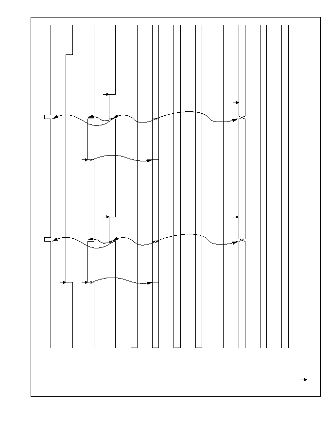
Interrupt (ADI)
ADIE
ADST
ADF
Channel 0 (AN )
0
Channel 1 (AN )
1
Channel 2 (AN )
2
Channel 3 (AN )
3
ADDRA
ADDRB
ADDRC
ADDRD
* indicates execution of a software instruction
Set*
Waiting
Waiting
Waiting
Waiting
A/D conver-
sion
A/D conver-
sion
Waiting
A/D conversion result
A/D conversion result
Waiting
A/D conversion starts
Set*
Set*
Clear*
Clear*
Read result
Read result
Figure 15-3 A/D Operation in Single Mode (When Channel 1 is Selected)
283

15.4.2 Scan Mode
The scan mode can be used to monitor analog inputs on one or more channels. When the ADST
bit is set to 1, A/D conversion starts from the first channel selected by the CH bits. When
CH2 = 0 the first channel is AN
0
. When CH2 = 1 the first channel is AN
4
.
If the scan group includes more than one channel (i.e. if bit CH1 or CH0 is set), conversion of the
next channel begins as soon as conversion of the first channel ends.
Conversion of the selected channels continues cyclically until the ADST bit is cleared to 0. The
conversion results are placed in the data registers corresponding to the selected channels.
Before selecting the scan mode, clock, and analog input channels, software should clear the ADST
bit to 0 to make sure the A/D converter is stopped. Changing the mode, clock, or channel
selection while A/D conversion is in progress can lead to conversion errors.
The following example explains the A/D conversion process when three channels in group 0 are
selected (AN
0
, AN
1
, and AN
2
). Figure 15-4 shows the corresponding timing chart.
1. Software clears the ADST bit to 0, then selects the scan mode (SCAN = 1), scan group 0
(CH2 = 0), and analog input channels AN
0
to AN
2
(CH1 and CH0 = 0) and sets the ADST bit
to 1 to start A/D conversion.
Coding Example: (with slow clock and ADI interrupt enabled)
BCLR #5, @H'FFE8
MOV.B #H'72, @FFE8
2. The A/D converter samples the input at AN
0
, converts the voltage level to a digital value, and
transfers the result to register ADDRA.
3. Next the A/D converter samples and converts AN
1
and transfers the result to ADDRB. Then it
samples and converts AN
2
and transfers the result to ADDRC.
4. After all selected channels (AN
0
to AN
2
) have been converted, the AD converter sets the ADF
bit to 1. If the ADIE bit is set to 1, an A/D interrupt (ADI) is requested. Then the A/D
converter begins converting AN
0
again.
5. Steps 2 to 4 are repeated cyclically as long as the ADST bit remains set to 1.
To stop the A/D converter, software must clear the ADST bit to 0.
284

Note on Scan Mode: If the ADST bit is cleared to 0 while two or more channels are being
converted in scan mode, incorrect values may be set in the A/D data registers.
This problem is limited to ZTAT versions. It does not occur in versions with masked ROM.
Solution: Read the A/D data registers only when the ADST bit is set to 1.
Example:
MOV.B #5B ,@ADCSR ; 4-channel scan mode
BSET.B #5 ,@ADCSR ; Start conversion (set ADST)
<A/D conversion continues>
ADI:
MOV.W @ADDRA , R0 ; read ADDRA
MOV.W @ADDRB , R1 ; read ADDRB
MOV.W @ADDRC , R2 ; read ADDRC
MOV.W @ADDRD , R3 ; read ADDRD
BCLR.B #5 , @ADCSR ; clear ADST
BCLR.B #7 , @ADCSR ; clear ADF
The A/D data registers should be read before ADST is cleared, as in the preceding example. (It is
not necessary to clear ADST in order to read the A/D data registers.)
285
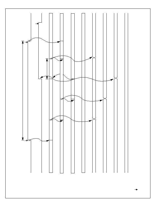
ADST
ADF
Channel 3 (AN )
3
Channel 0 (AN )
0
Channel 1 (AN )
1
Channel 2 (AN )
2
ADDRA
ADDRB
ADDRC
ADDRD
* indicates execution of a software instruction
Waiting
Waiting
Waiting
Set*
Continuous A/D conversion
Transfer
A/D conver-
sion
Waiting
A/D conver-
sion
A/D conversion
time
Clear*
Clear*
A/D conver-
sion
A/D conver-
sion
A/D conver-
sion
Waiting
A/D conversion
A/D conversion
A/D conversion
A/D conver-
sion
Waiting
Waiting
Waiting
Waiting
Figure 15-4 A/D Operation in Scan Mode (When Channels 0 to 2 are Selected)
286

15.5 Input Sampling Time and A/D Conversion Time
The A/D converter includes a built-in sample-and-hold circuit. Sampling of the input starts at a
time t
D
after the ADST bit is set to 1. The sampling process lasts for a time t
SPL
. The actual A/D
conversion begins after sampling is completed. Figure 15-5 shows the timing of these steps, and
table 15-4 lists the total conversion times (t
CONV
) for the single mode.
The total conversion time includes t
D
and t
SPL
. The purpose of t
D
is to synchronize the ADCSR
write time with the A/D conversion process, so the length of t
D
is variable. The total conversion
time therefore varies within the minimum to maximum ranges indicated in table 15-4.
In the scan mode, the ranges given in table 15-4 apply to the first conversion. The length of the
second and subsequent conversion processes is fixed at 256 states (when CKS = 0) or 128 states
(when CKS = 1).
287
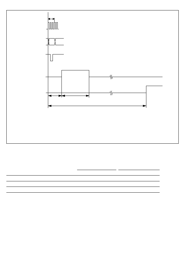
Table 15-4 A/D Conversion Time (Single Mode)
CKS = "0"
CKS = "1"
Item
Symbol
Min
Typ
Max
Min
Typ
Max
Synchronization delay
t
D
18
--
33
10
--
17
Input sampling time
t
SPL
--
63
--
--
31
--
Total A/D conversion time
t
CONV
259
--
274
131
--
138
Note: Values in the table are numbers of states.
Internal address
bus
Write signal
Input sampling
timing
ADF
¯
(1)
(2)
t
D
t
SPL
t
CONV
(1)
(2)
t
t
t
: ADCSR write cycle
: ADCSR address
: Synchronization delay
: Input sampling time
: Total A/D conversion time
D
SPL
CONV
Figure 15-5 A/D Conversion Timing
288

15.6 Interrupts and the Data Transfer Controller
The ADI interrupt request is enabled or disabled by the ADIE bit in the ADCSR.
When the ADI bit in data transfer enable register DTED (bit 0 at address H'FFF7) is set to 1, the
ADI interrupt is served by the data transfer controller. The DTC can be used to transfer A/D
results to a buffer in memory, or to an I/O port. The DTC automatically clears the ADF bit to 0.
Note: In scan mode, the DTC can transfer data for only one channel per interrupt, even if two or
more channels are selected.
289
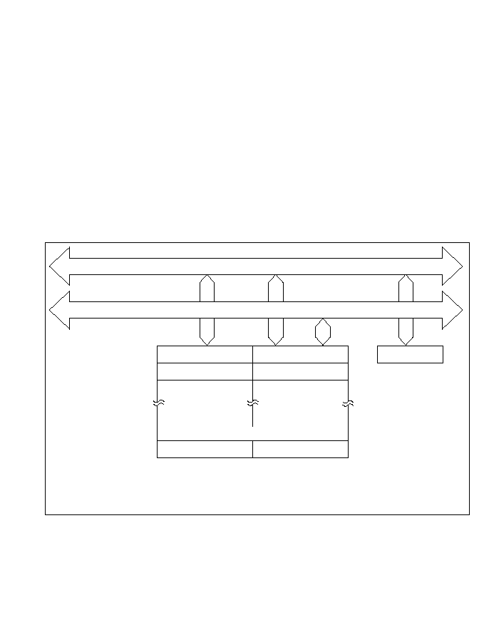
Section 16 RAM
16.1 Overview
The H8/532 includes 1K byte of on-chip static RAM, connected to the CPU by a 16-bit data bus.
Both byte and word access to the on-chip RAM are performed in two states, enabling rapid data
transfer and instruction execution.
The on-chip RAM is assigned to addresses H'FB80 to H'FF7F in the chip's address space. A
RAM control register (RAMCR) can enable or disable the on-chip RAM, permitting these
addresses to be allocated to external memory instead, if so desired.
16.1.1 Block Diagram
Figure 16-1 shows the block diagram of the on-chip RAM.
Internal data bus (upper 8 bits)
Internal data bus (lower 8 bits)
On-chip RAM
Address
H'FB80
H'FB82
H'FF7E
RAMCR
Even addresses
Odd addresses
RAMCR: RAM Control Register
Figure 16-1 Block Diagram of On-Chip RAM
291

16.1.2 Register Configuration
The on-chip RAM is controlled by the register described in table 16-1.
Table 16-1 RAM Control Register
Name
Abbreviation
R/W
Initial Value
Address
RAM control register
RAMCR
R/W
H'FF
H'FFF9
16.2 RAM Control Register (RAMCR)
The RAM control register (RAMCR) is an 8-bit register that enables or disable the on-chip RAM.
Bit 7--RAM Enable (RAME): This bit enables or disables the on-chip RAM.
The RAME bit is initialized on the rising edge of the signal. It is not initialized in the software
standby mode.
Bit 7
RAME
Description
0
On-chip RAM is disabled.
1
On-chip RAM is enabled.
(Initial value)
Bits 6 to 0--Reserved: These bits cannot be modified and are always read as 1.
16.3 Operation
16.3.1 Expanded Modes (Modes 1, 2, 3, and 4)
If the RAME bit is set to 1, accesses to addresses H'FB80 to H'FF7F are directed to the on-chip
RAM. If the RAME bit is cleared to 0, accesses to addresses H'FB80 to H'FF7F are directed to
the external data bus.
Bit
7
6
5
4
3
2
1
0
RAME
--
--
--
--
--
--
--
Initial value
1
1
1
1
1
1
1
1
Read/Write
R/W
--
--
--
--
--
--
--
292

16.3.2 Single-Chip Mode (Mode 7)
If the RAME bit is set to 1, accesses to addresses H'FB80 to H'FF7F are directed to the on-chip
RAM. If the RAME bit is cleared to 0, access of any type (instruction fetch or data read or write)
to addresses H'FB80 to H'FF7F causes an address error and initiates the CPU's exception-handling
sequence.
293

Section 17 ROM
17.1 Overview
The H8/532 includes 32K bytes of high-speed, on-chip ROM. The on-chip ROM is connected to
the CPU via a 16-bit data bus and is accessed in two states.
Users wishing to program the chip themselves can request electrically programmable ROM
(PROM). The PROM version of the H8/532 has a PROM mode in which the chip can be
programmed with a standard, external PROM writer. The chip is also available with masked
ROM.
The on-chip ROM is enabled or disabled depending on the MCU operating mode, which is
determined by the inputs at the mode pins when the chip comes out of the reset state.
See table 17-1.
Table 17-1 ROM Usage in Each MCU Mode
Mode Pins
Mode
MD
2
MD
1
MD
0
ROM
Mode 1 (expanded minimum mode)
0
0
1
Disabled (external addresses)
Mode 2 (expanded minimum mode)
0
1
0
Enabled
Mode 3 (expanded maximum mode)
0
1
1
Disabled (external addresses)
Mode 4 (expanded maximum mode)
1
0
0
Enabled
Mode 7 (single-chip mode)
1
1
1
Enabled
17.1.1 Block Diagram
Figure 17-1 shows the block diagram of the on-chip ROM.
295
17.2 PROM Mode
17.2.1 PROM Mode Setup
The PROM version of the H8/532 has a PROM mode in which the usual microcomputer functions
are halted to allow the on-chip PROM to be programmed. The programming method is the same
as for the HN27C256.
To select the PROM mode, apply the signal inputs listed in table 17-2.
Table 17-2 Selection of PROM Mode
Pin
Input
Mode pins (MD
2
, MD
1
, and MD
0
)
Low
STBY pin
Low
P6
1
and P6
0
High
Internal data bus (upper 8 bits)
Internal data bus (lower 8 bits)
On-chip ROM
Addresses
Even addresses
Odd addresses
H'0002
H'7FFF
H'0000
Figure 17-1 Block Diagram of On-Chip ROM
296

17.2.2 Socket Adapter Pin Arrangements and Memory Map
The H8/532 can be programmed with a general-purpose PROM writer by attaching a socket
adapter as listed in table 17-3. The socket adapter depends on the type of package. Figure 17-2
shows the socket adapter pin arrangements by giving the correspondence between H8/532 pins
and HN27C256 pin functions. Figure 17-3 is a memory map.
Table 17-3 Socket Adapter
Package
Socket Adapter
84-Pin PLCC (CP-84)
HS538ESC01H
84-Pin windowed LCC (CG-84)
HS538ESG01H
80-Pin plastic QFP (FP-80A)
HS538ESH01H
297

V
PP:
Programming power (12.5V)
E
7
to E
0
:
Data input/output
EA
14
to EA
0
: Address input
OE:
Output enable
CE:
Chip enable
∑
∑
∑
∑
∑
∑
∑
∑
∑
∑
∑
∑
∑
∑
Note: All pins not shown in this figure should be left open.
H8/532
HN27C256 (28 pins)
V
PP
1
EA
9
24
EO
0
11
EO
1
12
EO
2
13
EO
3
15
EO
4
16
EO
5
17
EO
6
18
EO
7
19
EA
0
10
EA
1
9
EA
2
8
EA
3
7
EA
4
6
EA
5
5
EA
6
4
EA
7
3
EA
8
25
OE
22
EA
10
21
EA
11
23
EA
12
2
EA
13
26
EA
14
27
CE
20
V
CC
28
Vss
14
EPROM socket
FP-80A
CG-84, CP-84
10
21
RES
11
22
NMI
13
25
P3
0
14
26
P3
1
15
27
P3
2
16
28
P3
3
17
29
P3
4
18
30
P3
5
19
31
P3
6
20
32
P3
7
21
33
P4
0
22
34
P4
1
23
35
P4
2
24
36
P4
3
25
37
P4
4
26
38
P4
5
27
39
P4
6
28
40
P4
7
30
43
P5
0
31
44
P5
1
32
45
P5
2
33
46
P5
3
34
47
P5
4
35
48
P5
5
36
49
P5
6
37
50
P5
7
38
51
P6
0
39
52
P6
1
60
74
AV
CC
5
16
V
CC
42
55
V
CC
6
17
MD
0
7
18
MD
1
8
19
MD
2
9
20
STBY
51
65
AV
ss
12
2
V
ss
29
24
V
ss
71
41
V
ss
--
42
V
ss
--
64
V
ss
--
83
V
ss
Figure 17-2 Socket Adapter Pin Arrangements
298

17.3 Programming
The write, verify, and inhibited sub-modes of the PROM mode are selected as shown in
table 17-4.
Table 17-4 Selection of Sub-Modes in PROM Mode
Pins
Mode
CE
OE
V
PP
V
CC
0
7
to 0
0
A
14
to A
0
Write
Low
High
V
PP
V
CC
Data input
Address input
Verify
High
Low
V
PP
V
CC
Data output
Address input
Programming inhibited
High
High
V
PP
V
CC
High-impedance
Address input
Note: The V
PP
and V
CC
pins must be held at the V
PP
and V
CC
voltage levels.
The H8/532 PROM uses the same, standard read/write specifications as the HN27C256 and
HN27256.
17.3.1 Writing and Verifying
An efficient, high-speed programming procedure can be used to write and verify PROM data.
This procedure writes data quickly without subjecting the chip to voltage stress and without
sacrificing data reliability. It leaves the data H'FF written in unused addresses.
On-chip ROM
Address in MCU mode
Address in PROM mode
H'0000
H'0000
H'7FFF
H'7FFF
Figure 17-3 Memory Map in PROM Mode
299
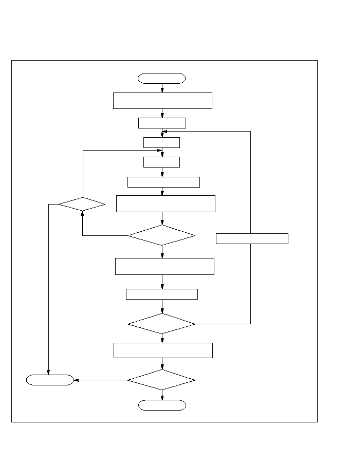
Figure 17-4 shows the basic high-speed programming flowchart.
Tables 17-5 and 17-6 list the electrical characteristics of the chip in the PROM mode. Figure 17-5
shows a write/verify timing chart.
SET program mode
Vcc = 6.0V ±0.25V, Vpp = 12.5V ±0.3V
Address = 0
n = 0
n + 1 1
Write time tpw = 1 ms ±5%
Verify OK?
N
N
Y
Y
SET verify mode
Vcc = 6.0V ±0.25V, Vpp = 12.5V ±0.3V
n < S
S = 25
Address + 1 Address
Last address?
N
Y
Write topw = 3n ms
SET program mode
Vcc = 6.0V ±0.25V, Vpp = 12.5V ±0.3V
SET read mode
Vcc = 5.0V ±0.5V, Vpp = Vcc
All address read?
END
NOGO
GO
Error
START
300
Figure 17-4 High-Speed Programming Flowchart

Table 17-5 DC Characteristics
(When V
CC
= 6.0V ±0.25V, V
PP
= 12.5V ±0.3V, V
SS
= 0V, Ta = 25∞C ±5∞C)
Sym-
Measurement
Item
bol
Min Typ Max
Unit Conditions
Input High voltage O
7
to O
0
, A
14
to A
0
, OE, CE V
IH
2.4
--
V
CC
+ 0.3 V
Input Low voltage
O
7
to O
0
, A
14
to A
0
, OE, CE V
IL
≠0.3 --
0.8
V
Input High voltage O
7
to O
0
V
OH
2.4
--
--
V
I
OH
=
≠200µA
Input Low voltage
O
7
to O
0
V
OL
--
--
0.45
V
I
OL
= 1.6mA
Input leakage
O
7
to O
0
, A
14
to A
0
, OE, CE |I
LI
|
--
--
2
µA
V
in
=
current
5.25V/0.5V
V
CC
current
I
CC
--
--
40
mA
V
PP
current
I
PP
--
--
40
mA
Table 17-6 AC Characteristics
(When V
CC
= 6.0V ±0.25V, V
PP
= 12.5V ±0.3V, Ta = 25∞C ±5∞C)
Sym-
Measurement
Item
bol
Min Typ Max
Unit Conditions
Address setup time
t
AS
2
--
--
µs
See figure
OE setup time
t
OES
2
--
--
µs
17-5
*
Data setup time
t
DS
2
--
--
µs
Address hold time
t
AH
0
--
--
µs
Data hold time
t
DH
2
--
--
µs
Data output disable time
t
DF
--
--
130
µs
V
PP
setup time
t
VPS
2
--
--
µs
Program pulse width
t
PW
0.95 1.0 1.05
ms
OE pulse width for
t
OPW
2.85 --
78.75
ms
overwrite-programming
V
CC
setup time
t
VCS
2
--
--
µs
Data output delay time
t
OE
0
--
500
ns
*
Input pulse level: 0.8V to 2.2V
Input rise/fall time
20ns
Timing reference levels: input--1.0V, 2.0V; output--0.8V, 2.0V
301

17.3.2 Notes on Writing
1. Write with the specified voltages and timing. The programming voltage (Vpp) in the
PROM mode is 12.5V.
Caution: Applied voltages in excess of the specified values can permanently destroy to the chip.
Be particularly careful about the PROM writer's overshoot characteristics.
If the PROM writer is set to Intel specifications or Hitachi HN27256 or HN27C256 specifications,
Vpp will be 12.5V.
2. Before writing data, check that the socket adapter and chip are correctly mounted in the
PROM writer. Overcurrent damage to the chip can result if the index marks on the PROM
writer, socket adapter, and chip are not correctly aligned.
GND
OE
CE
Write
Verify
Address
Data
Input data
Output data
V
pp
V
pp
V
cc
V
cc
V
cc
t
AS
t
DS
t
VPS
t
VCS
t
DH
t
PW
t
OES
t
OE
t
OPW
t
AH
t
DF
Figure 17-5 PROM Write/Verify Timing
302
3. Don't touch the socket adapter or chip while writing. Touching either of these can cause
contact faults and write errors.
17.3.3 Reliability of Written Data
An effective way to assure the data holding characteristics of the programmed chips is to bake
them at 150∞C, then screen them for data errors. This procedure quickly eliminates chips with
PROM memory cells prone to early failure.
Figure 17-6 shows the recommended screening procedure.
If a series of write errors occur while the same PROM writer is in use, stop programming and
check the PROM writer and socket adapter for defects, using a microcomputer with a windowed
package and on-chip EPROM.
Please inform Hitachi of any abnormal conditions noted during programming or in screening of
program data after high-temperature baking.
Write program
Bake with power off
150
∞
C 48 Hr
Read and check program
V
CC
= 4.5V and 5.5V
Install
Figure 17-6 Recommended Screening Procedure
303

17.3.4 Erasing of Data
The windowed package enables data to be erased by illuminating the window with ultraviolet
light. Table 17-7 lists the erasing conditions.
Table 17-7 Erasing Conditions
Item
Value
Ultraviolet wavelength
253.7nm
Minimum illumination
15W∑s/cm
2
The conditions in table 17-7 can be satisfied by placing a 12000µW/cm
2
ultraviolet lamp 2 or 3
centimeters directly above the chip and leaving it on for about 20 minutes.
17.4 Handling of Windowed Packages
1. Glass Erasing Window: Rubbing the glass erasing window of a windowed package with a
plastic material or touching it with an electrically charged object can create a static charge on
the window surface which may cause the chip to malfunction.
If the erasing window becomes charged, the charge can be neutralized by a short exposure to
ultraviolet light. This returns the chip to its normal condition, but it also reduces the charge
stored in the floating gates of the PROM, so it is recommended that the chip be reprogrammed
afterward.
Accumulation of static charge on the window surface can be prevented by the following
precautions:
(1) When handling the package, ground yourself. Don't wear gloves. Avoid other possible
sources of static charge.
(2) Avoid friction between the glass window and plastic or other materials that tend to
accumulate static charge.
(3) Be careful when using cooling sprays, since they may have a slight ion content.
(4) Cover the window with an ultraviolet-shield label, preferably a label including a
conductive material. Besides protecting the PROM contents from ultraviolet light, the label
protects the chip by distributing static charge uniformly.
2. Handling after Programming: Fluorescent light and sunlight contain small amounts of
ultraviolet, so prolonged exposure to these types of light can cause programmed data to invert.
304

In addition, exposure to any type of intense light can induce photoelectric effects that may lead
to chip malfunction. It is recommended that after programming the chip, you cover the erasing
window with a light-proof label (such as an ultraviolet-shield label).
3. 84-Pin LCC Package Mounting: When mounted on a printed circuit board, the 84-pin LCC
package must be mounted in a socket. The recommended socket is listed in table 17-8.
Table 17-8 Socket for 84-Pin LCC Package
Manufacturer
Product Code
Sumitomo 3-M
284-1273-00-1102J
305

Section 18 Power-Down State
18.1 Overview
The H8/532 has a power-down state that greatly reduces power consumption by stopping the CPU
functions. The power-down state includes three modes:
1. Sleep mode--
a software-triggered mode in which the CPU halts but the rest of
the chip remains active
2. Software standby mode--
a software-triggered mode in which the entire chip is inactive
3. Hardware standby mode--
a hardware-triggered mode in which the entire chip is inactive
The sleep mode and software standby mode are entered from the program execution state by
executing the SLEEP instruction under the conditions given in table 18-1. The hardware standby
mode is entered from any other state by a Low input at the STBY pin.
Table 18-1 lists the conditions for entering and leaving the power-down modes. It also indicates
the status of the CPU, on-chip supporting modules, etc., in each power-down mode.
Table 18-1 Power-Down State
Entering
CPU
Sup.
I/O
Exiting
Mode
Procedure
Clock
CPU
Reg's.
Mod's.
RAM
Ports
Methods
Sleep Execute
Run
Halt
Held
Run
Held
Held
∑
Interrupt
mode
SLEEP
∑ RES Low
instruction
∑ STBY Low
Soft-
Set SSBY bit
Halt
Halt
Held
Halt
Held
Held
∑ NMI
ware
in SBYCR to
and
∑ RES Low
standby
1, then
partly
∑ STBY Low
mode
execute SLEEP
initialized
instruction
*
Hard-
Set STBY
Halt
Halt
Not
Halt
Held
High
∑ STBY High,
ware
pin to Low
held
and
impe-
then RES
standby
level
partly
dance
Low
High
mode
initialized
state
*
The watchdog timer must also be stopped.
Notes: SBYCR Software standby control register
SSBY
Software standby bit
307

18.2 Sleep Mode
18.2.1 Transition to Sleep Mode
Execution of the SLEEP instruction causes a transition from the program execution state to the
sleep mode. After executing the SLEEP instruction, the CPU halts, but the contents of its internal
registers remain unchanged. The functions of the on-chip supporting modules do not stop in the
sleep mode.
18.2.2 Exit from Sleep Mode
The chip wakes up from the sleep mode when it receives an internal or external interrupt request,
or a Low input at the RES or STBY pin.
1. Wake-Up by Interrupt: An interrupt releases the sleep mode and starts either the CPU's
interrupt-handling sequence or the data transfer controller (DTC).
If the interrupt is served by the DTC, after the data transfer is completed the CPU executes the
instruction following the SLEEP instruction, unless the count in the data transfer count register
(DTCR) is 0.
If an interrupt on a level equal to or less than the mask level in the CPU's status register (SR) is
requested, the interrupt is left pending and the sleep mode continues. Also, if an interrupt from
an on-chip supporting module is disabled by the corresponding enable/disable bit in the
module's control register, the interrupt cannot be requested, so it cannot wake the chip up.
2. Wake-Up by RES pin: When the RES pin goes Low, the chip exits from the sleep mode to the
reset state.
3. Wake-Up by STBY pin: When the STBY pin goes Low, the chip exits from the sleep mode to
the hardware standby mode.
18.3 Software Standby Mode
18.3.1 Transition to Software Standby Mode
A program enters the software standby mode by setting the standby bit (SSBY) in the software
standby control register (SBYCR) to 1, then executing the SLEEP instruction. Table 18-2 lists the
attributes of the software standby control register.
308

Table 18-2 Software Standby Control Register
Name
Abbreviation
R/W
Initial Value
Address
Software standby control register
SBYCR
R/W
H'7F
H'FFFB
In the software standby mode, the CPU, clock, and the on-chip supporting module functions all
stop, reducing power consumption to an extremely low level. The on-chip supporting modules
and their registers are reset to their initial state, but as long as a minimum necessary voltage
supply is maintained (at least 2V), the contents of the CPU registers and on-chip RAM remain
unchanged. The I/O ports also remain in their current states.
18.3.2 Software Standby Control Register (SBYCR)
The software standby control register (SBYCR) is an 8-bit register that controls the action of the
SLEEP instruction.
Bit 7--Software Standby (SSBY): This bit enables or disables the transition to the software
standby mode.
Bit 7
SSBY
Description
0
The SLEEP instruction causes a transition to the sleep mode. (Initial value)
1
The SLEEP instruction causes a transition to the software standby mode.
The watchdog timer must be stopped before the chip can enter the software standby mode. To
stop the watchdog timer, clear the timer enable bit (TME) in the watchdog timer's timer
control/status register (TCSR) to 0. The SSBY bit cannot be set to 1 while the TME bit is set to 1.
When the chip is recovered from the software standby mode by a nonmaskable interrupt (NMI),
the SSBY bit is automatically cleared to 0. It is also cleared to 0 by a reset or transition to the
hardware standby mode.
Bits 6 to 0--Reserved: These bits cannot be modified and are always read as 1.
Bit
7
6
5
4
3
2
1
0
SSBY
--
--
--
--
--
--
--
Initial value
0
1
1
1
1
1
1
1
Read/Write
R/W
--
--
--
--
--
--
--
309

18.3.3 Exit from Software Standby Mode
The chip can be brought out of the software standby mode by an input at one of three pins: the
NMI pin, RES pin, or STBY pin.
1. Recovery by NMI Pin: When an NMI request signal is received, the clock oscillator begins
operating but clock pulses are supplied only to the watchdog timer (WDT). The watchdog
timer begins counting from H'00 at the rate determined by the clock select bits (CKS2 to
CKS0) in its timer status/control register (TCSR). This rate should be set slow enough to allow
the clock oscillator to stabilize before the count reaches H'FF. When the count overflows from
H'FF to H'00, clock pulses are supplied to the whole chip, the software standby mode ends, and
execution of the NMI interrupt-handling sequence begins.
The clock select bits (CKS2 to CKS0) should be set as follows.
(1) Crystal oscillator: Set CKS2 to CKS0 to a value that makes the watchdog timer interval
equal to or greater than 10ms, which is the clock stabilization time.
(2) External clock input: CKS2 to CKS0 can be set to any value. The minimum value
(CKS2 = CKS1 = CKS0 = 0) is recommended.
2. Recovery by RES Pin: When the RES pin goes Low, the clock oscillator starts. Next, when
the RES pin goes High, the CPU begins executing the reset sequence.
When the chip recovers from the software standby mode by a reset, clock pulses are supplied to
the entire chip at once. Be sure to hold the RES pin Low long enough for the clock to stabilize.
3. Recovery by STBY Pin: When STBY the pin goes Low, the chip exits from the software
standby mode to the hardware standby mode.
18.3.4 Sample Application of Software Standby Mode
In this example the chip enters the software standby mode on the falling edge of the NMI input
and recovers from the software standby mode on the rising edge of NMI. Figure 18-1 shows a
timing chart of the transitions.
The nonmaskable interrupt edge bit (NMIEG) in the port 1 control register (P1CR) is originally
cleared to 0, selecting the falling edge as the NMI trigger. After accepting an NMI interrupt in
this condition, software changes the NMIEG bit to 1, sets the SSBY bit to 1, and executes the
SLEEP instruction to enter the software standby mode. The chip recovers from the software
standby mode on the next rising edge at the NMI pin.
310

18.3.5 Application Notes
(1) The I/O ports retain their current states in the software standby mode. If a port is in the High
output state, its output current is not reduced in the software standby mode.
(2) If the software standby mode is entered under either condition or condition below in a
ZTAT version of the H8/532, current dissipation is greater than in normal standby mode (I
CC
=
100 to 300µA). This problem does not occur in H8/532 versions with masked ROM.
In single-chip mode (mode 3): if software standby mode is entered after even one
instruction not stored in on-chip ROM has been fetched (e.g. from on-chip RAM).
In expanded mode with on-chip ROM enabled (mode 2): if software standby mode is
entered after even one instruction not stored in on-chip ROM has been fetched (e.g. from
external memory or on-chip RAM).
This problem does not occur in the expanded mode when on-chip ROM is disabled (mode 1).
In applications in which the additional standby current must be avoided, take one of the
following actions:
NMI
NMEG
SSBY
¯
NMI interrupt handling
NMIEG = 1
SSBY = 1
SLEEP instruction
Software standby mode
(Power-down state)
Clock start-up
time
Clock setting time
WDT overflow
NMI interrupt handling
Oscillator
WDT interval (t )
OSC2
Figure 18-1 NMI Timing of Software Standby Mode (Application Example)
311

∑
Store program code only in on-chip ROM.
∑
Use the hardware standby mode. There is never any additional current in hardware standby
mode.
18.4 Hardware Standby Mode
18.4.1 Transition to Hardware Standby Mode
Regardless of its current state, the chip enters the hardware standby mode whenever the STBY pin
goes Low.
The hardware standby mode reduces power consumption drastically by halting the CPU, stopping
all the functions of the on-chip supporting modules, and placing I/O ports in the high-impedance
state.
The registers of the on-chip supporting modules are reset to their initial values. Only the on-chip
RAM is held unchanged, provided the minimum necessary voltage supply is maintained (at least
2V).*
Notes: 1
The RAME bit in the RAM control register should be cleared to 0 before the STBY
pin goes Low, to disable the on-chip RAM during the hardware standby mode.
2
Do not change the inputs at the mode pins (MD2, MD1, MD0) during hardware
standby mode. Be particularly careful not to let all three mode inputs go low, since
that would place the chip in PROM mode, causing increased current dissipation.
18.4.2 Recovery from Hardware Standby Mode
Recovery from the hardware standby mode requires inputs at both the STBY and RES pins.
When the STBY pin goes High, the clock oscillator begins running. The RES pin should be Low
at this time and should be held Low long enough for the clock to stabilize. When the RES pin
changes from Low to High, the reset sequence is executed and the chip returns to the program
execution state.
312

18.4.3 Timing Sequence of Hardware Standby Mode
Figure 18-2 shows the usual sequence for entering and leaving the hardware standby mode.
First the RES pin goes Low, placing the chip in the reset state. Then the STBY pin goes Low,
placing the chip in the hardware standby mode and stopping the clock. In the recovery sequence
first the STBY pin goes High; then after the clock stabilizes, the RES pin is returned to the High
level.
Oscillator
RES
STBY
Clock setting time
Restart
Figure 18-2 Hardware Standby Sequence
313

Section 19 E Clock Interface
19.1 Overview
For interfacing to E clock based peripheral devices, the H8/532 can generate an E clock output.
Special instructions (MOVTPE, MOVFPE) perform data transfers synchronized with the E clock.
The E clock is created by dividing the system clock (¯) by 8. The E clock is output at the P1
1
pin
when the P1
1
DDR bit in the port 1 data direction register (P1DDR) is set to 1.
When the CPU executes an instruction that synchronizes with the E clock, the address is output on
the address bus as usual, but the data bus and the R/W, DS, RD, and WR signal lines do not
become active until the falling edge of the E clock is detected. The length of the access cycle for
an instruction synchronized with the E clock is accordingly variable. Figures 19-1 and 19-2 show
the timing in the cases of maximum and minimum synchronization delay.
The wait state controller (WSC) does not insert any wait states (Tw) during the execution of an
instruction synchronized with the E clock.
315

AS,
T
1
T
2
T
E
T
E
T
E
T
E
T
E
T
E
T
E
T
E
T
E
T
E
T
E
T
E
T
E
T
E
T
3
Last state
E
¯
A to A
19
0
R/W
DS (Read access),
RD
DS (Write access),
WR
D to D
(Read access)
70
D to D
(Write access)
70
Figure 19-1 Execution Cycle of Instruction Synchronized with E Clock in
Expanded Modes (Maximum Synchronization Delay)
Figure 19-1 Execution Cycle of Instruction Synchronized with E Clock in
Expanded Modes (Maximum Synchronization Delay)
316

AS,
T
1
T
2
T
E
T
E
T
E
T
E
T
E
T
E
T
E
T
3
Last state
E
¯
A to A
19
0
R/W
DS (Read access),
RD
DS (Write access),
WR
D to D
(Read access)
7
0
D to D
(Write access)
7
0
Figure 19-2 Execution Cycle of Instruction Synchronized with E Clock in Expanded Modes
(Minimum Synchronization Delay)
317

Section 20 Electrical Specifications
20.1 Absolute Maximum Ratings
Table 20-1 lists the absolute maximum ratings.
Table 20-1 Absolute Maximum Ratings
Item
Symbol
Rating
Unit
Supply voltage
V
CC
≠0.3 to +7.0
V
Programming voltage
V
PP
≠0.3 to +13.5
V
Input voltage (except Port 8)
V
in
≠0.3 to V
CC
+ 0.3
V
(Port 8)
V
in
≠0.3 to AV
CC
+ 0.3
V
Analog supply voltage
AV
CC
≠0.3 to +7.0
V
Analog input voltage
V
AN
≠0.3 to AV
CC
+ 0.3
V
Operating temperature
T
opr
Regular specifications: ≠20 to +75
∞C
Wide-range specifications: ≠40 to +85
∞C
Storage temperature
T
stg
≠55 to +125
∞C
Note: Permanent LSI damage may occur if maximum ratings are exceeded. Normal operation
should be under recommended operating conditions.
20.2 Electrical Characteristics
20.2.1 DC Characteristics
Table 20-2 lists the DC characteristics.
319

Table 20-2 DC Characteristics
Conditions: V
CC
= 5.0V ±10%
*1
, AV
CC
= 5.0V ±10%, V
SS
= AV
SS
= 0V,
T
a
= ≠20 to +75∞C (Regular Specifications)
T
a
= ≠40 to +85∞C (Wide-Range Specifications)
Sym-
Measurement
Item
bol
Min
Typ
Max
Unit Conditions
Input High voltage RES, STBY,
V
IH
V
CC
≠ 0.7
≠
V
CC
+0.3
V
MD
2
, MD
1
, MD
0
EXTAL
V
CC
◊
0.7
≠
V
CC
+0.3
V
Port 8
2.2
≠
AV
CC
+0.3 V
Other input pins
2.2
≠
V
CC
+0.3
V
(except port 7)
Input Low voltage
RES, STBY,
V
IL
≠0.3
≠
0.5
V
MD
2
, MD
1
, MD
0
Other input pins
≠0.3
≠
0.8
V
(except port 7)
Schmitt trigger
Port 7
V
T-
1.0
≠
2.5
V
input voltage
V
T+
2.0
≠
3.5
V
V
T+
≠V
T-
0.4
≠
≠
V
Input leakage
RES
| I
in
|
≠
≠
10.0
µA
V
in
= 0.5 to
current
STBY, NMI,
≠
≠
1.0
µA
V
CC
≠0.5V
MD
2
, MD
1
, MD
0
port 8
≠
≠
1.0
µA
V
in
= 0.5 to
AV
CC
≠0.5V
Leakage current
Port 9,
| I
TSI
|
≠
≠
1.0
µA
V
in
= 0.5 to
in 3-state
ports 7 to 1
V
CC
≠0.5V
(off state)
Input pull-up
ports 6 and 5
≠I
P
50
≠
200
µA
V
in
= 0V
MOS current
Output High
All output pins
V
OH
V
CC
≠0.5
≠
≠
V
I
OH
= ≠200µA
Voltage
3.5
≠
≠
V
I
OH
= ≠1mA
Output Low
All output pins
V
OL
≠
≠
0.4
V
I
OL
= 1.6mA
Voltage
Port 4
≠
≠
1.0
V
I
OL
= 8mA
≠
≠
1.2
V
I
OL
= 10mA
Input capacitance
RES
C
in
≠
≠
60
pF
V
in
= 0 V
NMI
≠
≠
30
pF
f = 1MHz
All input pins
≠
≠
15
pF
T
a
= 25∞C
except RES, NMI
Note:
*
1 AVcc must be connected to a power supply line, even when the A/D converter is not used.
*
1
320

Table 20-2 DC Characteristics (cont)
Sym-
Measurement
Item
bol
Min
Typ
Max
Unit
Conditions
Current dissipation
Normal operation
I
CC
≠
20
30
mA
f = 6 MHz
≠
25
40
mA
f = 8 MHz
≠
30
50
mA
f = 10 MHz
Sleep mode
≠
12
20
mA
f = 6 MHz
≠
16
25
mA
f = 8 MHz
≠
20
30
mA
f = 10 MHz
Standby
≠
0.01
5.0
µA
T
a
50∞C
≠
≠
20
µA
T
a
> 50∞C
Analog supply
During A/D
AI
CC
≠
1.2
2.0
mA
current
conversion
While waiting
≠
0.01
5.0
µA
RAM standby voltage
V
RAM
2.0
≠
≠
V
*
2 Current dissipation values assume that V
IH
min = V
CC
≠ 0.5V, V
IL
max = 0.5V, all output pins are
in the no-load state, and all MOS input pull-ups are off.
Table 20-3 Allowable Output Current Sink Values
Conditions: V
CC
= 5.0V ±10%, AV
CC
= 5.0V ±10%, V
SS
= AV
SS
= 0V,
T
a
= ≠20 to +75∞C (Regular Specifications)
T
a
= ≠40 to +85∞C (Wide-Range Specifications)
Item
Symbol
Min
Typ
Max
Unit
Allowable output Low
Port 4
I
OL
≠
≠
10
mA
current sink (per pin)
Other output pins
≠
≠
2.0
mA
Allowable output Low
Port 4, total of 8 pins
I
OL
≠
≠
40
mA
current sink (total)
Total of all other
≠
≠
80
mA
output pins
Allowable output High
All output pins
≠I
OH
≠
≠
2.0
mA
current sink (per pin)
Allowable output High
Total of all output
≠I
OH
≠
≠
25
mA
current sink (total)
pins
Note: To avoid degrading the reliability of the chip, be careful not to exceed the output current sink
values in table 20-3. In particular, when driving a Darlington transistor pair or LED directly,
be sure to insert a current-limiting resistor in the output path. See figures 20-1 and 20-2.
*
2
321

20.2.2 AC Characteristics
The AC characteristics of the H8/532 chip are listed in three tables. Bus timing parameters are
given in table 20-4, control signal timing parameters in table 20-5, and timing parameters of the
on-chip supporting modules in table 20-6.
Table 20-4 Bus Timing
Conditions: V
CC
= 5.0V ±10%, AV
CC
= 5.0V ±10%, ¯ = 0.5 to 10MHz, V
SS
= 0V
T
a
= ≠20 to +75∞C (Regular Specifications)
T
a
= ≠40 to +85∞C (Wide-Range Specifications)
6MHz
8MHz
10MHz
Measurement
Item
Symbol Min
Max
Min
Max
Min Max Unit Conditions
Clock cycle time
t
cyc
166.7 2000
125
2000 100 2000 ns
See figure 20-4
Clock pulse width Low
t
CL
65
≠
45
≠
35
≠
ns
Clock pulse width High
t
CH
65
≠
45
≠
35
≠
ns
Clock rise time
t
Cr
≠
15
≠
15
≠
15
ns
Clock fall time
t
Cf
≠
15
≠
15
≠
15
ns
Address delay time
t
AD
≠
70
≠
65
≠
65
ns
Address hold time
t
AH
30
≠
25
≠
20
≠
ns
Data strobe delay time 1
t
DSD1
≠
70
≠
60
≠
40
ns
Data strobe delay time 2
t
DSD2
≠
70
≠
60
≠
50
ns
Data strobe delay time 3
t
DSD3
≠
70
≠
60
≠
50
ns
Write data strobe pulse width
t
DSWW
200
≠
150
≠
120 ≠
ns
Address setup time 1
t
AS1
25
≠
20
≠
15
≠
ns
- - - - - - - - - - - - -
- - - - - - - - - - - - -
- - - - - - -
- - -
- - - - - - -
- - -
H8/532
Port
2 k
Darlington pair
Vcc
600
LED
Port 4
H8/532
Figure 20-1 Example of Circuit for Driving a
Darlington Transistor Pair
Figure 20-2 Example of Circuit for Driving
an LED
322

Table 20-4 Bus Timing (cont)
6MHz
8MHz
10MHz
Measurement
Item
Symbol Min
Max
Min
Max
Min Max
Unit Conditions
Address setup time 2
t
AS2
105
≠
80
≠
65
≠
ns
See figure 20-4
Read data setup time
t
RDS
60
≠
50
≠
40
≠
ns
Read data hold time
t
RDH
0
≠
0
≠
0
≠
ns
Read data access time
t
ACC
≠
280
≠
190
≠
160
ns
Write data delay time
t
WDD
≠
70
≠
65
≠
65
ns
Write data setup time
t
WDS
30
≠
15
≠
10
≠
ns
Write data hold time
t
WDH
30
≠
25
≠
20
≠
ns
Wait setup time
t
WTS
40
≠
40
≠
40
≠
ns
See figure 20-5
Wait hold time
t
WTH
10
≠
10
≠
10
≠
ns
Bus request setup time
t
BRQS
40
≠
40
≠
40
≠
ns
See figure 20-10
Bus acknowledge delay time 1 t
BACD1
≠
70
≠
60
≠
55
ns
Bus acknowledge delay time 2 t
BACD2
≠
70
≠
60
≠
55
ns
Bus floating delay time
t
BZD
≠
t
BACD1
≠
t
BACD1
≠
t
BACD1
ns
E clock delay time
t
ED
≠
20
≠
15
≠
15
ns
See figure 20-
11
E clock rise time
t
Er
≠
15
≠
15
≠
15
ns
E clock fall time
t
Ef
≠
15
≠
15
≠
15
ns
Read data hold time
t
RDHE
0
≠
0
≠
0
≠
ns
See figure 20-6
(E clock sync)
Write data hold time
t
WDHE
50
≠
40
≠
30
≠
ns
(E clock sync)
323

Table 20-5 Control Signal Timing
Conditions: V
CC
= 5.0V ±10%, AV
CC
= 5.0V ±10%, ¯ = 0.5 to 10MHz, V
SS
= 0V
T
a
= ≠20 to +75∞C (Regular Specifications)
T
a
= ≠40 to +85∞C (Wide-Range Specifications)
6MHz
8MHz
10MHz
Measurement
Item
Symbol Min
Max
Min
Max
Min Max
Unit Conditions
RES setup time
t
RESS
200
≠
200
≠
200 ≠
ns
See figure 20-7
RES pulse width
t
RESW
6.0
≠
6.0
≠
6.0
≠
t
cyc
Mode programming
t
MDS
4.0
≠
4.0
≠
4.0
≠
t
cyc
setup time
NMI setup time
t
NMIS
150
≠
150
≠
150 ≠
ns
See figure 20-8
NMI hold time
t
NMIH
10
≠
10
≠
10
≠
ns
IRQ
0
setup time
t
IRQ0S
50
≠
50
≠
50
≠
ns
IRQ
1
setup time
t
IRQ1S
50
≠
50
≠
50
≠
ns
IRQ
1
hold time
t
IRQ1H
10
≠
10
≠
10
≠
ns
NMI pulse width
t
NMIW
200
≠
200
≠
200 ≠
ns
See figure 20-9
(for recovery from
software standby mode)
Crystal oscillator settling
t
OSC1
20
≠
20
≠
20
≠
ms
See figure 20-12
time (reset)
Crystal oscillator settling time t
OSC2
10
≠
10
≠
10
≠
ms
See figure 18-1
(software standby)
324
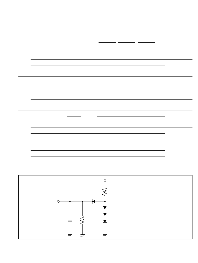
Table 20-6 Timing Conditions of On-Chip Supporting Modules
Conditions: V
CC
= 5.0V ±10%, AV
CC
= 5.0V ±10%, ¯ = 0.5 to 10MHz, V
SS
= 0V
T
a
= ≠20 to +75∞C (Regular Specifications)
T
a
= ≠40 to +85∞C (Wide-Range Specifications)
6MHz
8MHz
10MHz
Measurement
Item
Symbol
Min
Max
Min
Max
Min Max Unit Conditions
FRT
Timer output delay time
t
FTOD
≠
100
≠
100
≠
100
ns
See figure 20-14
Timer input setup time
t
FTIS
50
≠
50
≠
50
≠
ns
Timer clock input setup time
t
FTCS
50
≠
50
≠
50
≠
ns
See figure 20-15
Timer clock pulse width
t
FTCWL
,
t
FTCWH
1.5
≠
1.5
≠
1.5
≠
t
cyc
TMR
Timer output delay time
t
TMOD
≠
100
≠
100
≠
100
ns
See figure 20-16
Timer clock input setup time
t
TMCS
50
≠
50
≠
50
≠
ns
See figure 20-17
Timer clock pulse width
t
TMCWL
,
t
TMCWH
1.5
≠
1.5
≠
1.5
≠
t
cyc
Timer reset input setup time
t
TMRS
50
≠
50
≠
50
≠
ns
See figure 20-18
PWM
Timer output delay time
t
PWOD
≠
100
≠
100
≠
100
ns
See figure 20-19
SCI
Input clock cycle
(Async)
t
Scyc
2
≠
2
≠
2
≠
t
cyc
See figure 20-20
(Sync)
4
≠
4
≠
4
≠
t
cyc
Input clock pulse width
t
SCKW
0.4
0.6
0.4
0.6
0.4
0.6
t
Scyc
Transmit data delay time (Sync)
t
TXD
≠
100
≠
100
≠
100
ns
See figure 20-21
Receive data setup time (Sync)
t
RXS
100
≠
100
≠
100 ≠
ns
Receive data hold time
(Sync)
t
RXH
100
≠
100
≠
100 ≠
ns
Port
Output data delay time
t
PWD
≠
100
≠
100
≠
100
ns
See figure 20-13
Input data setup time
t
PRS
50
≠
50
≠
50
≠
ns
Input data hold time
t
PRH
50
≠
50
≠
50
≠
ns
∑ Measurement Conditions for AC Characteristics
H8/532
output pin
5 V
C
R
H
C
R
R
Input/output timing reference levels
Low:
High:
= 90 pF: P1, P2, P3, P4, P5, P6
= 30 pF: P7, P9
= 2.4 k
= 12 k
0.8V
2.0V
L
H
R
L
C = 90 pF: P1, P2, P3, P4, P5, P6
= 30 pF: P7, P9
R
L
= 2.4 k
R
H
= 12 k
Input/output timing reference levels
Low: 0.8V
High: 2.0V
Figure 20-3 Output Load Circuit
325

20.2.3 A/D Converter Characteristics
Table 20-7 lists the characteristics of the on-chip A/D converter.
Table 20-7 A/D Converter Characteristics
Conditions: V
CC
= 5.0V ±10%, AV
CC
= 5.0V ±10%, V
SS
= AV
SS
= 0V,
T
a
= ≠20 to +75∞C (Regular Specifications)
T
a
= ≠40 to +85∞C (Wide-Range Specifications)
6MHz
8MHz
10MHz
Item
Min
Typ Max
Min
Typ Max
Min Typ Max
Unit
Resolution
10
10
10
10
10
10
10
10
10
Bits
Conversion time
--
--
23.0
--
--
17.25 --
--
13.8
µs
Analog input capacitance
--
--
20
--
--
20
--
--
20
pF
Allowable signal-source impedance
--
--
10
--
--
10
--
--
10
k
Nonlinearity error
--
--
±2.0
--
--
±2.0
--
--
±2.0
LSB
Offset error
--
--
±2.0
--
--
±2.0
--
--
±2.0
LSB
Full-scale error
--
--
±2.0
--
--
±2.0
--
--
±2.0
LSB
Quantizing error
--
--
±0.5
--
--
±0.5
--
--
±0.5
LSB
Absolute accuracy
--
--
±2.5
--
--
±2.5
--
--
±2.5
LSB
20.3 MCU Operational Timing
This section provides the following timing charts:
20.3.1 Bus timing
Figures 20-4 to 20-6
20.3.2 Control Signal Timing
Figures 20-7 to 20-10
20.3.3 Clock Timing
Figures 20-11 and 20-12
20.3.4 I/O Port Timing
Figure 20-13
20.3.5 16-Bit Free-Running Timer Timing
Figures 20-14 and 20-15
20.3.6 8-Bit Timer Timing
Figures 20-16 to 20-18
20.3.7 Pulse Width Modulation Timer Timing
Figure 20-19
20.3.8 Serial Communication InterfaceTiming
Figure 20-20 and 20-21
326

20.3.1 Bus Timing
1. Basic Bus Cycle (without Wait States) in Expanded Modes
AS,
¯
A to A
19
0
R/W
DS (Read),
RD
DS (Write),
D to D
(Read)
7
0
D to D
(Write)
7
0
WR
t
CH
t
cyc
T
1
T
2
T
3
t
CL
t
AD
t
Cf
t
Cr
t
DSD1
t
AS1
t
ACC
t
DSD2
t
AS2
t
WDS
t
WDD
t
DSD3
t
DSWW
t
RDS
t
RDH
t
WDH
t
AH
t
AH
t
DSD3
Figure 20-4 Basic Bus Cycle (without Wait States) in Expanded Modes
327
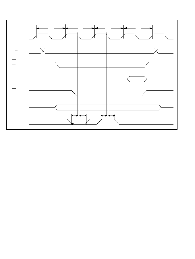
2. Basic Bus Cycle (with 1 Wait State) in Expanded Modes
T
1
T
2
T
W
T
3
¯
A to A
19
0
R/W
DS (Read),
RD
DS (Write),
D to D
(Read)
7
0
D to D
(Write)
7
0
WR
WAIT
t
WTS
t
WTH
t
WTS
t
WTH
Figure 20-5 Basic Bus Cycle (with 1 Wait State) in Expanded Modes
328
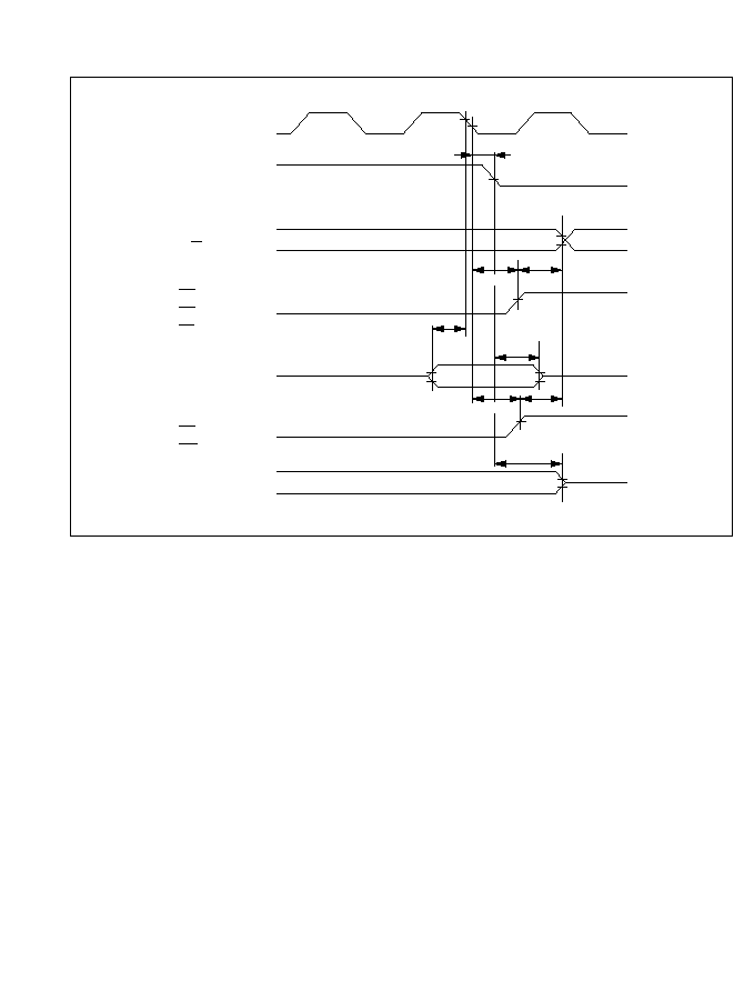
3. Bus Cycle Synchronized with E Clock
¯
A to A
19
0
R/W
DS (Read),
RD
D to D (Read)
7
0
D to D (Write)
7
0
DS (Write),
WR
AS,
E
t
RDS
t
WDHE
t
AH
t
RDHE
t
ED
t
DSD3
t
AH
t
DSD3
Figure 20-6 Bus Cycle Synchronized with E Clock
329

20.3.2 Control Signal Timing
1. Reset Input Timing
2. Interrupt Input Timing
3. NMI Pulse Width
RES
¯
t
RESW
t
MDS
MD to MD
2
0
t
RESS
t
RESS
IRQ
0
IRQ
1
NMI
¯
t
IRQ1S
t
IRQ0S
t
IRQ1H
t
NMIH
t
NMIS
NMI
t
NMIW
Figure 20-7 Reset Input Timing
Figure 20-8 Interrupt Input Timing
Figure 20-9 NMI Pulse Width (for Recovery from Software Standby Mode)
330
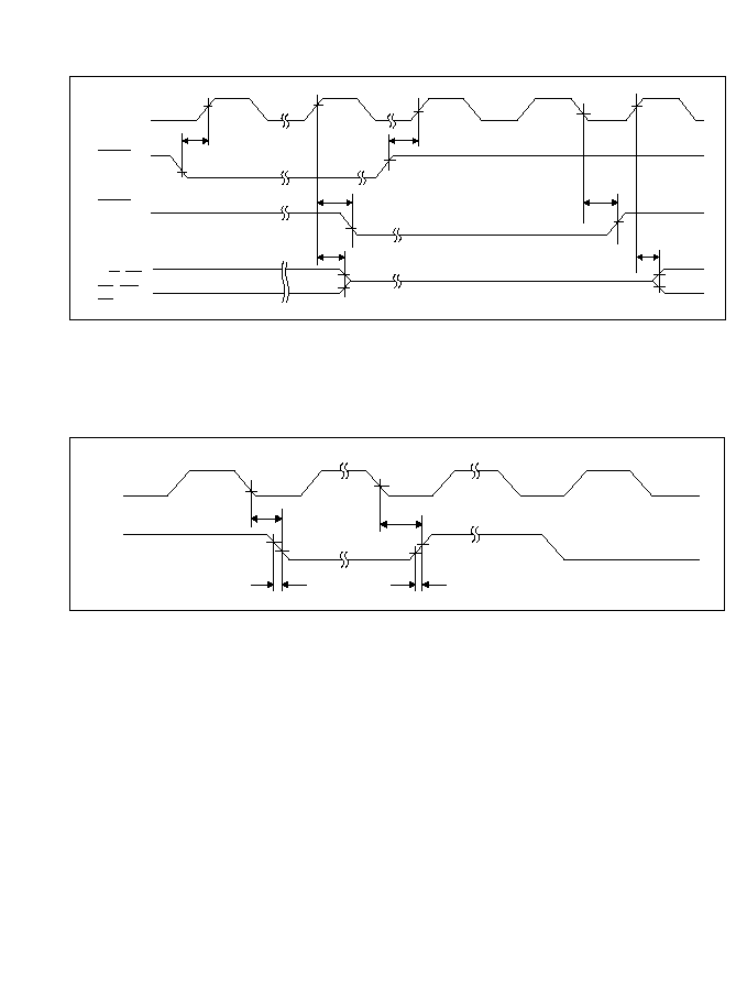
4. Bus Release State Timing
20.3.3 Clock Timing
1. E Clock Timing
BREQ
(Input)
¯
BACK
(Output)
A to A ,
R/W, DS,
RD, WR,
AS
19
0
t
BRQS
t
BACD1
t
BZD
t
BRQS
t
BACD2
t
AD
¯
E
t
Ef
t
ED
t
ED
t
Er
Figure 20-10 Bus Release State Timing
Figure 20-11 E Clock Timing
331
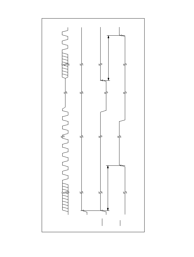
2. Clock Oscillator Stabilization Timing
STBY
RES
V
CC
¯
t
OSC1
t
OSC1
Figure 20-12 Clock Oscillator Stabilization Timing
332
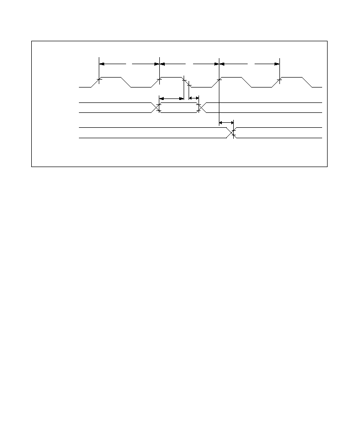
20.3.4 I/O Port Timing
t
PRS
t
PRH
t
PWD
T
1
T
2
T
3
Port 1
to (Input)
port 9
Port 1*
to (Output)
port 9
* Except P1 , P1 , and P8 to P8
1
0
7
0
Port read/write cycle
¯
Figure 20-13 I/O Port Input/Output Timing
333

20.3.5 16-Bit Free-Running Timer Timing
1. Free-Running Timer Input/Output Timing
2. External Clock Input Timing for Free-Running Timers
t
FTOD
¯
Free-running
timer counter
FTOA , FTOB ,
1
1
FTOA , FTOB ,
2
2
FTOA , FTOB
3
3
FTI , FTI , FTI
1
3
2
Compare-match
t
FTIS
t
FTCS
t
FTCWL
t
FTCWH
FTCI ,
1
¯
FTCI ,
2
FTCI
3
Figure 20-14 Free-Running Timer Input/Output Timing
Figure 20-15 External Clock Input Timing for Free-Running Timers
334
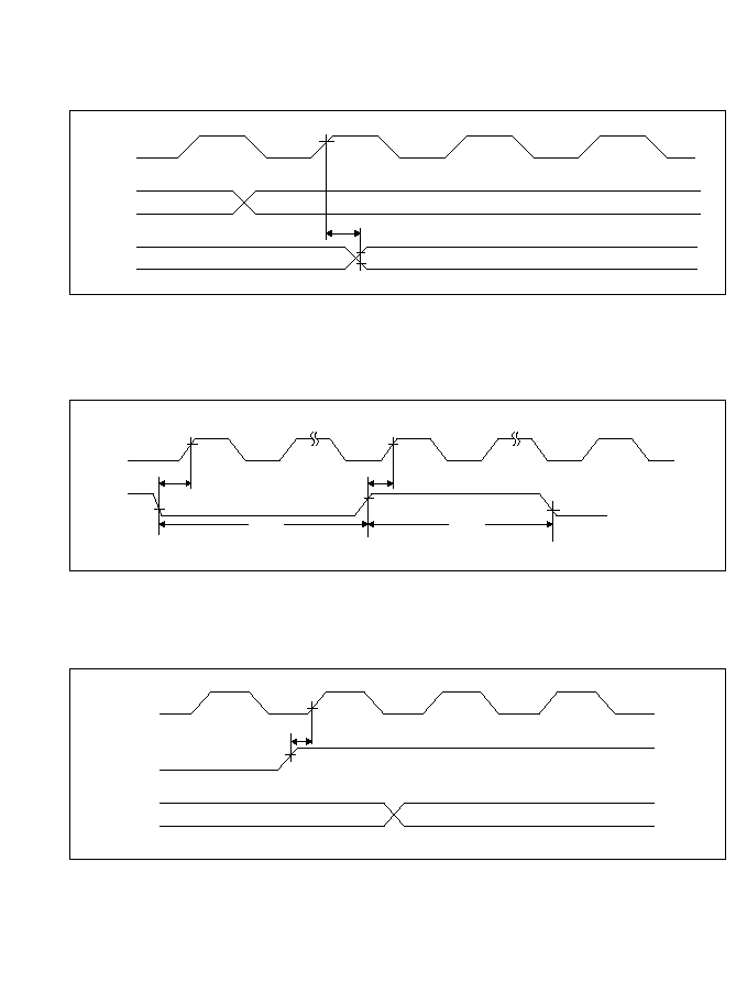
20.3.6 8-Bit Timer Timing
1. 8-Bit Timer Output Timing
2. 8-Bit Timer Clock Input Timing
3. 8-Bit Timer Reset Input Timing
t
TMOD
¯
Timer
counter
TMO
Compare-match
¯
TMCI
t
TMCS
t
TMCS
t
TMCWL
t
TMCWH
t
TMRS
n
¯
TMRI
Timer
counter
H'00
Figure 20-16 8-Bit Timer Output Timing
Figure 20-17 8-Bit Timer Clock Input Timing
Figure 20-18 8-Bit Timer Reset Input Timing
335

20.3.7 Pulse Width Modulation Timer Timing
20.3.8 Serial Communication Interface Timing
PW , PW ,
1
t
PWOD
Compare-match
¯
Timer
counter
2
PW
3
t
SCKW
t
Scyc
t
Scyc
t
rXD
t
RXS
t
RXH
Serial clock
Transmit
data
Receive
data
Figure 20-19 PWM Timer Output Timing
Figure 20-20 SCI Input Clock Timing
Figure 20-21 SCI Input/Output Timing (Synchronous Mode)
336

Appendix A Instructions
A.1 Instruction Set
Operation Notation
Rd
General register (destination operand)
FP
Frame pointer
Rs
General register (source operand)
#IMM
Immediate data
Rn
General register
disp
Displacement
(EAd)
Destination operand
+
Add
(EAs)
Source operand
≠
Subtract
CCR
Condition code register
◊
Multiply
N
N (Negative) flag in CCR
˜
Divide
Z
Z (Zero) flag in CCR
Logical AND
V
V (Overflow) flag in CCR
Logical OR
C
C (Carry) flag in CCR
Logical exclusive OR
CR
Control register
Move
PC
Program counter
Swap
CP
Code page register
¨
Logical NOT
SP
Stack pointer
Condition Code Notation
§
Changed after instruction execution
0
Cleared to 0
1
Set to 1
--
Value before operation is retained
Changed depending on condition
337

Size
CCR Bit
Mnemonic
Operation
B/W
N
Z
V
C
Data
MOV: G
(EAs)
Rd
B/W
§
§
0
--
transfer
Rs
(EAd)
#IMM
(EAd)
MOV: E
#IMM
Rd
(short format)
B
§
§
0
--
MOV: F
@ (d: 8, FP)
Rd
B/W
§
§
0
--
Rs
@ (d: 8, FP)(short format)
MOV: I
#IMM
Rd
(short format)
W
§
§
0
--
MOV: L
(@aa: 8)
Rd
(short format)
B/W
§
§
0
--
MOV: S
Rs
(@aa: 8)
(short format)
B/W
§
§
0
--
LDM
@ SP +
Rn (register list)
W
--
-- --
--
STM
Rn (register list)
@ ≠ SP
W
--
-- --
--
XCH
Rs
Rd
W
--
-- --
--
SWAP
Rd (upper byte)
Rd (lower byte)
B
§
§
0
--
MOVTPE
Rs
(EAd) Synchronized with E clock B
--
-- --
--
MOVFPE
(EAs)
Rd Synchronized with E clock B
--
-- --
--
Arith-
ADD: G
Rd + (EAs)
Rd
B/W
§
§
§
§
metic
ADD: Q
(EAd) + #IMM
(EAd)
B/W
§
§
§
§
opera-
(#IMM = ±1, ±2)
(short format)
tions
ADDS
Rd + (EAs)
Rd
B/W
--
-- --
--
(Rd is always word size)
ADDX
Rd + (EAs) + C
Rd
B/W
§
§
§
§
DADD
(Rd)
10
+ (Rs)
10
+ C
(Rd)
10
B
--
§
--
§
SUB
Rd ≠ (EAs)
Rd
B/W
§
§
§
§
SUBS
Rd ≠ (EAs)
Rd
B/W
--
-- --
--
SUBX
Rd ≠ (EAs) ≠ C
Rd
B/W
§
§
§
§
DSUB
(Rd)
10
≠ (Rs)
10
≠ C
(Rd)
10
B
--
§
--
§
MULXU
Rd
◊
(EAs)
Rd
8
◊
8
B/W
§
§
0
0
(Unsigned)
16
◊
16
DIVXU
Rd
˜
(EAs)
Rd
16
˜
8
B/W
§
§
§
0
(Unsigned)
32
˜
16
CMP: G
Rd ≠ (EAs), Set CCR
B/W
§
§
§
§
(EAd) ≠ #IMM, Set CCR
CMP: E
Rd ≠ #IMM, Set CCR
(short format)
B
§
§
§
§
CMP: I
Rd ≠ #IMM, Set CCR
(short format)
W
§
§
§
§
338

Size
CCR Bit
Mnemonic
Operation
B/W
N
Z
V
C
Arith-
EXTS
(< Bit 7 > of < Rd >)
B
§
§
0
0
metic
(< Bit 15 to 8 > of < Rd >)
opera-
EXTU
0
(<Bit 15 to 8 > of < Rd >)
B
0
§
0
0
tions
TST
(EAd) ≠ 0, Set CCR
B/W
§
§
0
0
NEG
0 ≠ (EAd)
(EAd)
B/W
§
§
0
§
CLR
0
(EAd)
B/W
0
1
0
0
TAS
(EAd) ≠ 0, Set CCR
B
§
§
0
0
(1)
2
(< Bit 7 > of < EAd >)
Shift
SHAL
B/W
§
§
§
§
opera-
tions
SHAR
B/W
§
§
0
§
SHLL
B/W
§
§
0
§
SHLR
B/W
0
§
0
§
ROTL
B/W
§
§
0
§
ROTR B/W
§
§
0
§
ROTXL B/W
§
§
0
§
ROTXR B/W
§
§
0
§
Logic
AND
Rd
(EAs)
Rd
B/W
§
§
0
--
opera-
OR
Rd
(EAs)
Rd
B/W
§
§
0
--
tions
XOR
Rd
(EAs)
Rd
B/W
§
§
0
--
NOT
¨ (EAd)
(EAd)
B/W
§
§
0
--
Bit
BSET
¨ (< Bit number > of < EAd >)
Z
B/W
--
§
--
--
manipu-
1
(< Bit number > of < EAd >)
lations
BCLR
¨ (< Bit number > of < EAd >)
Z
B/W
--
§
--
--
0
(< Bit number > of < EAd >)
BTST
¨ (< Bit number > of < EAd >)
Z
B/W
--
§
--
--
BNOT
¨ (< Bit number > of < EAd >)
Z
B/W
--
§
--
--
(< Bit number > of < EAd >)
MSB
LSB
MSB
LSB
MSB
LSB
MSB
LSB
MSB
LSB
MSB
LSB
MSB
LSB
MSB
LSB
C
C
C
C
0
C
C
0
0
C
C
339

Size
CCR Bit
Mnemonic
Operation
B/W
N
Z
V
C
Branch- Bcc
If condition is true then
--
--
--
--
--
ing
PC + disp
PC
instruc-
else next;
tions
JMP
Effective address
PC
--
--
-- --
--
PJMP
Effective address
CP, PC
--
--
-- --
--
BSR
PC
@ ≠ SP
--
--
-- --
--
PC + disp
PC
JSR
PC
@ ≠ SP
--
--
-- --
--
Effective address
PC
PJSR
PC
@ ≠ SP
--
--
-- --
--
CP
@ ≠ SP
Effective address
CP, PC
RTS
@ SP +
PC
--
--
-- --
--
PRTS
@ SP +
CP
--
--
-- --
--
@ SP +
PC
RTD
@ SP +
PC
--
--
-- --
--
SP + #IMM
SP
PRTD
@ SP +
CP
--
--
-- --
--
@ SP +
PC
SP + #IMM
SP
SCB
If condition is true then next;
--
--
-- --
--
SCB/F
else Rn ≠ 1
Rn;
SCB/NE If Rn = ≠1 then next;
SCB/EQ
else PC + disp
PC;
Mnemonic
Description
Condition
BRA
(BT)
Always (True)
True
BRN
(BF)
Never (False)
False
BHI
HIgh
C
Z = 0
BLS
Low or Same
C
Z = 0
Bcc
(BHS)
Carry Clear (High or Same)
C = 0
BCS
(BLO)
Carry Set (LOw)
C = 1
BNE
Not Equal
Z = 0
BEQ
EQual
Z = 1
BVC
oVerflow Clear
V = 0
BVS
oVerflow Set
V = 1
BPL
PLus
N = 0
BMI
MInus
N = 1
BGE
Greater or Equal
N
V = 0
BLT
Less Than
N
V = 1
BGT
Greater Than
Z
(N
V) = 0
BLE
Less or Equal
Z
(N
V) = 1
Mnemonic
Description
Condition
SCB/F
False
SCB/NE
Not Equal
Z = 0
SCB/EQ
Equal
Z = 1
340
Size
CCR Bit
Mnemonic
Operation
B/W
N
Z
V
C
System TRAPA
PC
@ ≠ SP
--
--
--
--
--
control
(If MAX MODE CP
@ ≠ SP)
SR
@ ≠ SP
(If MAX MODE < vector >
CP)
< vector >
PC
TRAP/VS If V bit = "1" then TRAP
--
--
--
--
--
else next;
RTE
@ SP +
SR
--
§
§
§
§
(If MAX MODE @ SP +
CP)
@ SP +
PC
LINK
FP (R6)
@ ≠ SP
--
--
--
--
--
SP
FP (R6)
SP + #IMM
SP
UNLK
FP (R6)
SP
--
--
--
--
--
@SP +
FP
SLEEP
Normal running mode
power-down state
--
--
--
--
--
LDC
(EAs)
CR
B/W
*
STC
CR
(EAd)
B/W
*
--
--
--
--
ANDC
CR
#IMM
CR
B/W
*
ORC
CR
#IMM
CR
B/W
*
XORC
CR
#IMM
CR
B/W
*
NOP
PC + 1
PC
--
--
--
--
--
*
Depends on the CR.
341
A.2 Instruction Codes
Table A-1 shows the machine-language coding of each instruction.
∑ How to read table A-1 (a) to (d)
The general operand format consists of an effective address (EA) field and operation-code (OP)
field specified in the following order.
EA field
Op field
1
2
3
4
5
6
Bytes 2, 3, 5, 6 are not present in all instructions.
342

Instruction
Operation code (OP)
Instruction
MOV:G.B <EA >, R
s
d
MOV:G.W <EA >, R
s
d
MOV:G.B R , <EA >
s
d
MOV:G.W R , <EA >
s
d
2
3
4
2
2
3
4
4 1 0 0 1 0 r r r
2
3
4
2
2
3
4
2
2
3
4
2
2
3
4
2
2
3
4
2
2
3
4
3
4
3
s
s s
1 0 0 1 0 r r r
s
s s
1 0 0 0 0 r r r
d d d
1 0 0 0 0 r r r
d d d
4
5
6
Byte length of instruction
Shading indicates addressing
modes not available for this
instruction.
Some instructions have a special format in which the operation code comes first.
The following notation is used in the tables.
∑ Sz:
Byte:
Word:
Operand size (byte or word)
Sz = 0
Sz = 1
Address-
ing mode
Rn
@Rn
@(d:8, Rn)
@(d:16, Rn)
@≠Rn
@Rn+
@aa:8
@aa:16
#xx:8
#xx:16
1 0 1 0 Sz r r r
1 1 0 1 Sz r r r
1 1 1 0 Sz r r r
1 1 1 1 Sz r r r
1 0 1 1 Sz r r r
1 1 0 0 Sz r r r
0 0 0 0 Sz 1 0 1
0 0 0 1 Sz 1 0 1
0 0 0 0 0 1 0 0
0 0 0 0 1 1 0 0
12
3
Operation code (EA)
disp
disp (H)
address
address (H)
data
data (H)
disp (L)
address (L)
data (L)
343
∑ rrr : General register number field
rrr
Sz = 0 (Byte)
Sz = 1 (Word)
15
8 7
0
15
0
000
Not used
R0
R0
001
Not used
R1
R1
010
Not used
R2
R2
011
Not used
R3
R3
100
Not used
R4
R4
101
Not used
R5
R5
110
Not used
R6
R6
111
Not used
R7
R7
∑ ccc : Control register number field
ccc
Sz = 0 (Byte)
Sz = 1 (Word)
000
(Not allowed
*
)
001
(Not allowed)
010
(Not allowed)
(Not allowed)
011
BR
(Not allowed)
100
EP
(Not allowed)
101
DP
(Not allowed)
110
(Not allowed)
(Not allowed)
111
TP
(Not allowed)
*
"Disallowed" means that this combination of bits must not be specified. Specifying a disallowed
combination may cause abnormal results.
344
15
0
SR
7
0
CCR
∑ register list: A byte in which bits indicate general registers as follows
∑ #VEC: Four bits designating a vector number from 0 to 15. The vector numbers correspond to
addresses of entries in the exception vector table as follows:
Vector Address
Vector Address
#VEC Minimum Mode
Maximum Mode
#VEC Minimum Mode
Maximum Mode
0
H'0020 ≠ H'0021
H'0040 ≠ H'0043
8
H'0030 ≠ H'0031
H'0060 ≠ H'0063
1
H'0022 ≠ H'0023
H'0044 ≠ H'0047
9
H'0032 ≠ H'0033
H'0064 ≠ H'0067
2
H'0024 ≠ H'0025
H'0048 ≠ H'004B
10
H'0034 ≠ H'0035
H'0068 ≠ H'006B
3
H'0026 ≠ H'0027
H'004C ≠ H'004F
11
H'0036 ≠ H'0037
H'006C ≠ H'006F
4
H'0028 ≠ H'0029
H'0050 ≠ H'0053
12
H'0038 ≠ H'0039
H'0070 ≠ H'0073
5
H'002A ≠ H'002B
H'0054 ≠ H'0057
13
H'003A ≠ H'003B
H'0074 ≠ H'0077
6
H'002C ≠ H'002D
H'0058 ≠ H'005B
14
H'003C ≠ H'003D
H'0078 ≠ H'007B
7
H'002E ≠ H'002F
H'005C ≠ H'005F
15
H'003E ≠ H'003F
H'007C ≠ H'007F
∑ Examples of machine-language coding
Example 1: ADD:G.B @R0, R1
EA Field
OP Field
Table A-1 (a)
1101Szrrr
00100r
d
r
d
r
d
Machine code
11010000
00100 0 0 1
H'D021
Example 2: ADD:G.W @H'11:8, R1
EA Field
OP Field
Table A-1 (a)
0000Sz101
00010001
00100r
d
r
d
r
d
Machine code
0000 1 101
00010001
00100 0 0 1
H'0D1121
Bit
7
6
5
4
3
2
1
0
R7
R6
R5
R4
R3
R2
R1
R0
345
Instruction
Operation code (OP)
Data transfer instruction
MOV:G.B <EA >, R
s
d
MOV:G.W <EA >, R
s
d
MOV:G.B R , <EA >
s
d
MOV:G.W R , <EA >
s
d
2
3
4
2
2
3
4
4 1 0 0 1 0
2
3
4
2
2
3
4
2
2
3
4
2
2
3
4
2
2
3
4
2
2
3
4
3
4
1 0 0 1 0
1 0 0 0 0
1 0 0 0 0
d
4
5
6
Note: Short format instruction
Address-
ing mode
Rn
@Rn
@(d:8, Rn)
@(d:16, Rn)
@≠Rn
@Rn+
@aa:8
@aa:16
#xx:8
#xx:16
1 0 1 0 Sz r r r
1 1 0 1 Sz r r r
1 1 1 0 Sz r r r
1 1 1 1 Sz r r r
1 0 1 1 Sz r r r
1 1 0 0 Sz r r r
0 0 0 0 Sz 1 0 1
0 0 0 1 Sz 1 0 1
0 0 0 0 0 1 0 0
0 0 0 0 1 1 0 0
12
3
Operation code (EA)
disp
disp (H)
address
address (H)
data
data (H)
disp (L)
address (L)
data (L)
MOV:G.B #xx:8, <EA >
d
3
4
5
3
3
4
5
0 0 0 0 0 1 1 0
r
d
r
d
r
d
r
d
r
d
r
s
r
s
r
s
r
s
r
s
r
s
r
data
MOV:G.W #xx:8, <EA >
d
3
4
5
3
3
4
5
0 0 0 0 0 1 1 0
data
MOV:G.W #xx:16, <EA >
d
4
5
6
4
4
5
6
0 0 0 0 0 1 1 1
data (H)
data (L)
LDM.W @SP+,
<register list>
2
0 0 0 0 0 0 1 0
register list
STM.W ,@≠SP
<register list>
2
0 0 0 0 0 0 1 0
register list
XCH.W R ,R
s
d
2
1 0 0 1 0
d
r
d
r
d
r
SWAP.B R
d
2
0 0 0 1 0 0 0 0
MOVTPE.B R , <EA >
s
d
3
4
5
3
3
4
5
0 0 0 0 0 0 0 0 1 0 0 1 0
s
r
s
r
s
r
MOVTPE.B <EA >, R
s
d
3
4
5
3
3
4
5
0 0 0 0 0 0 0 0 1 0 0 1 0
d
r
d
r
d
r
Arithmetic operation instruction
ADD:G.B <EA >, R
s
d
2
2
3
4
2
2
3
4
3
0 0 1 0 0
d
r
d
r
d
r
ADD:G.W <EA >, R
d
2
2
3
4
2
2
3
4
4 0 0 1 0 0
d
r
d
r
d
r
s
ADD:Q.B #1, <EA >
d
2
2
3
4
2
2
3
4
0 0 0 0 1 0 0 0
*
ADD:Q.W #1, <EA >
d
2
2
3
4
2
2
3
4
0 0 0 0 1 0 0 0
*
ADD:Q.B #2, <EA >
d
2
2
3
4
2
2
3
4
0 0 0 0 1 0 0 1
*
ADD:Q.W #2, <EA >
d
2
2
3
4
2
2
3
4
0 0 0 0 1 0 0 1
*
ADD:Q.B #-1, <EA >
d
2
2
3
4
2
2
3
4
0 0 0 0 1 1 0 0
*
ADD:Q.W #-1, <EA >
d
2
2
3
4
2
2
3
4
0 0 0 0 1 1 0 0
*
ADD:Q.B #-2, <EA >
d
2
2
3
4
2
2
3
4
0 0 0 0 1 1 0 1
*
ADD:Q.W #-2, <EA >
d
2
2
3
4
2
2
3
4
0 0 0 0 1 1 0 1
*
ADDS.B <EA >, R
d
2
2
3
4
2
2
3
4
3
0 0 1 0 1
d
r
d
r
d
r
s
ADDS.W <EA >, R
d
2
2
3
4
2
2
3
4
4 0 0 1 0 1
d
r
d
r
d
r
s
ADDX.B <EA >, R
d
2
2
3
4
2
2
3
4
3
1 0 1 0 0
d
r
d
r
d
r
s
ADDX.W <EA >, R
d
2
2
3
4
2
2
3
4
4 1 0 1 0 0
d
r
d
r
d
r
s
*
Table A-1 (a) Machine Language Coding [General Format]
346
Instruction
Operation code (OP)
DADD.B R ,R
s
d
SUB.B <EA >, R
s
d
SUB.W <EA >, R
s
d
SUBS.B <EA >, R
s
d
2
3
4
2
2
3
4
0 0 1 1 1
2
3
4
2
2
3
4
2
2
3
4
2
2
3
4
4
3
0 0 1 1 0
0 0 1 1 0
0 0 0 0 0 0 0 0
4
5
6
Address-
ing mode
Rn
@Rn
@(d:8, Rn)
@(d:16, Rn)
@≠Rn
@Rn+
@aa:8
@aa:16
#xx:8
#xx:16
1 0 1 0 Sz r r r
1 1 0 1 Sz r r r
1 1 1 0 Sz r r r
1 1 1 1 Sz r r r
1 0 1 1 Sz r r r
1 1 0 0 Sz r r r
0 0 0 0 Sz 1 0 1
0 0 0 1 Sz 1 0 1
0 0 0 0 0 1 0 0
0 0 0 0 1 1 0 0
12
3
Operation code (EA)
disp
disp (H)
address
address (H)
data
data (H)
disp (L)
address (L)
data (L)
SUBS.W <EA >,R
d
2
3
4
2
2
3
4
0 0 1 1 1
d
r
d
r
d
r
d
r
d
r
d
r
d
r
d
r
d
r
SUBX.B <EA >, R
d
2
3
4
2
2
3
4
1 0 1 1 0
data
SUBX.W <EA >, R
d
2
3
4
2
2
3
4
1 0 1 1 0
data (H)
data (L)
DSUB.B R , R
0 0 0 0 0 0 0 0
MULXU.B <EA >, R
s
2
1 0 1 0 1
MULXU.X <EA >, R
s
d
2
1 0 1 0 1
d
r
d
r
d
r
DIVXU.B <EA >, R
d
2
1 0 1 1 1
DIVXU.W <EA >, R
s
d
2
3
4
2
2
3
4
1 0 1 1 1
CMP:G.B <EA >, R
s
d
3
4
5
3
3
4
5
0 1 1 1 0
1 0 1 0 0
d
r
d
r
d
r
Arithmetic operation instruction
CMP:G.W <EA >, R
s
d
2
2
3
4
2
2
3
4
3
0 1 1 1 0
d
r
d
r
d
r
CMP:G.B #xx, <EA >
d
3
4
5
3
3
4
5
0 0 0 0 0 1 0 0
CMP:G.W #xx, <EA >
d
4
5
6
4
4
5
6
0 0 0 0 0 1 0 1
EXTS.B R
d
2
0 0 0 1 0 0 0 1
EXTU.B R
d
2
0 0 0 1 0 0 1 0
TST.B <EA >
d
2
2
3
4
2
2
3
4
0 0 0 1 0 1 1 0
TST.W <EA >
d
2
2
3
4
2
2
3
4
0 0 0 1 0 1 1 0
NEG.B <EA >
d
2
2
3
4
2
2
3
4
0 0 0 1 0 1 0 0
NEG.W <EA >
d
2
2
3
4
2
2
3
4
0 0 0 1 0 1 0 0
CLR.B <EA >
d
2
2
3
4
2
2
3
4
0 0 0 1 0 0 1 1
CLR.W <EA >
d
2
2
3
4
2
2
3
4
0 0 0 1 0 0 1 1
TAS.B <EA >
d
2
2
3
4
2
2
3
4
0 0 0 1 0 1 1 1
s
s
s
d
s
d
s
4
3
4
3
4
2
2
2
3
2
2
3
4
4
2
3
2
2
3
4
4
2
3
2
3
4
4
2
3
2
4
2
3
2
4
2
3
2
1 0 1 1 0
d
r
d
r
d
r
d
r
d
r
d
r
d
r
d
r
d
r
d
r
d
r
d
r
d
r
d
r
d
r
d
r
d
r
d
r
d
r
d
r
d
r
d
r
d
r
d
r
Table A-1 (a) Machine Language Coding [General Format] (cont)
347
Instruction
Operation code (OP)
SHAL.B <EA >
d
SHAL.W <EA >
d
SHAR.B <EA >
d
SHAR.W <EA >
d
2
3
4
2
2
3
4
0 0 0 1 1 0 0 1
2
3
4
2
2
3
4
2
2
3
4
2
2
3
4
0 0 0 1 1 0 0 1
0 0 0 1 1 0 0 0
0 0 0 1 1 0 0 0
4
5
6
Address-
ing mode
Rn
@Rn
@(d:8, Rn)
@(d:16, Rn)
@≠Rn
@Rn+
@aa:8
@aa:16
#xx:8
#xx:16
1 0 1 0 Sz r r r
1 1 0 1 Sz r r r
1 1 1 0 Sz r r r
1 1 1 1 Sz r r r
1 0 1 1 Sz r r r
1 1 0 0 Sz r r r
0 0 0 0 Sz 1 0 1
0 0 0 1 Sz 1 0 1
0 0 0 0 0 1 0 0
0 0 0 0 1 1 0 0
12
3
Operation code (EA)
disp
disp (H)
address
address (H)
data
data (H)
disp (L)
address (L)
data (L)
SHLL.B <EA >
d
2
3
4
2
2
3
4
0 0 0 1 1 0 1 0
SHLL.W <EA >
d
2
3
4
2
2
3
4
0 0 0 1 1 0 1 0
SHLR.B <EA >
d
2
3
4
2
2
3
4
0 0 0 1 1 0 1 1
SHLR.W <EA >
0 0 0 1 1 0 1 1
ROTL.B <EA >
2
0 0 0 1 1 1 0 0
ROTL.W <EA >
d
2
0 0 0 1 1 1 0 0
d
r
d
r
d
r
ROTR.B <EA >
d
2
0 0 0 1 1 1 0 1
ROTR.W <EA >
d
2
3
4
2
2
3
4
0 0 0 1 1 1 0 1
ROTXL.B <EA >
d
2
3
4
2
2
3
4
0 0 0 1 1 1 1 0
Shift instruction
ROTXL.W <EA >
d
2
2
3
4
2
2
3
4
3
0 0 0 1 1 1 1 0
d
r
d
r
d
r
ROTXR.B <EA >
d
2
3
4
2
2
3
4
0 0 0 1 1 1 1 1
ROTXR.W <EA >
d
2
3
4
2
2
3
4
0 0 0 1 1 1 1 1
AND.B <EA >, R
d
2
0 1 0 1 0
AND.W <EA >, R
d
2
0 1 0 1 0
OR.B.B <EA >, R
d
2
2
3
4
2
2
3
4
0 1 0 0 0
OR.B.W <EA >, R
d
2
2
3
4
2
2
3
4
0 1 0 0 0
XOR.B <EA >, R
d
2
2
3
4
2
2
3
4
0 1 1 0 0
XOR.W <EA >, R
d
2
2
3
4
2
2
3
4
0 1 1 0 0
NOT.B <EA >
d
2
2
3
4
2
2
3
4
0 0 0 1 0 1 0 1
NOT.W <EA >
d
2
2
3
4
2
2
3
4
0 0 0 1 0 1 0 1
d
d
4
3
4
3
4
2
2
2
3
2
2
3
4
4
2
3
2
2
3
4
4
2
3
2
3
4
4
2
2
2
2
2
2
2
d
r
d
r
d
r
d
r
d
r
d
r
d
r
d
r
d
r
d
r
d
r
d
r
Logic operation instruction
s
s
s
s
s
s
2
3
4
2
2
3
4
2
3
4
2
2
3
4
2
2
2
2
3
2
3
4
4
2
2
3
4
2
2
3
4
Table A-1 (a) Machine Language Coding [General Format] (cont)
348

Instruction
Operation code (OP)
BSET.B #xx, <EA >
d
BSET.W #xx, <EA >
d
BSET.B R , <EA >
d
BSET.W R , <EA >
s
2
3
4
2
2
3
4
0 1 0 0 1
2
3
4
2
2
3
4
2
2
3
4
2
2
3
4
0 1 0 0 1
1 1 0 0
1 1 0 0
4
5
6
Address-
ing mode
Rn
@Rn
@(d:8, Rn)
@(d:16, Rn)
@≠Rn
@Rn+
@aa:8
@aa:16
#xx:8
#xx:16
1 0 1 0 Sz r r r
1 1 0 1 Sz r r r
1 1 1 0 Sz r r r
1 1 1 1 Sz r r r
1 0 1 1 Sz r r r
1 1 0 0 Sz r r r
0 0 0 0 Sz 1 0 1
0 0 0 1 Sz 1 0 1
0 0 0 0 0 1 0 0
0 0 0 0 1 1 0 0
12
3
Operation code (EA)
disp
disp (H)
address
address (H)
data
data (H)
disp (L)
address (L)
data (L)
BCLR.B #xx, <EA >
d
2
3
4
2
2
3
4
1 1 0 1
BCLR.W #xx, <EA >
d
2
3
4
2
2
3
4
1 1 0 1
BCLR.B R , <EA >
s
2
3
4
2
2
3
4
0 1 0 1 1
BCLR.W R , <EA >
0 1 0 1 1
BTST.B #xx, <EA >
2
1 1 1 1
BTST.W #xx, <EA >
d
2
1 1 1 1
BTST.B R , <EA >
s
2
0 1 1 1 1
BTST.W R , <EA >
s
2
3
4
2
2
3
4
0 1 1 1 1
BNOT.B #xx, <EA >
d
2
3
4
2
2
3
4
1 1 1 0
Bit manipulate instruction
BNOT.W #xx, <EA >
d
2
2
3
4
2
2
3
4
1 1 1 0
BNOT.B R , <EA >
s
2
3
4
2
2
3
4
0 1 1 0 1
BNOT.W R , <EA >
s
2
3
4
2
2
3
4
0 1 1 0 1
LDC.B <EA >, CR
2
1 0 0 0 1 c c c
LDC.W <EA >, CR
2
1 0 0 0 1 c c c
STC.B CR, <EA >
d
2
2
3
4
2
2
3
4
1 0 0 1 1 c c c
STC.W CR, <EA >
d
2
2
3
4
2
2
3
4
1 0 0 1 1 c c c
ANDC.B #xx:8, CR
0 1 0 1 1 c c c
ANDC.W #xx:16, CR
0 1 0 1 1 c c c
ORC.B #xx:8, CR
0 1 0 0 1 c c c
ORC.W #xx:16, CR
0 1 0 0 1 c c c
d
3
4
3
4
2
2
2
3
2
2
3
4
4
2
3
2
2
3
4
4
2
3
2
3
4
4
2
2
2
2
2
2
2
System control instruction
s
s
2
3
4
2
2
3
4
2
3
4
2
2
3
4
2
2
2
2
3
2
3
4
4
2
2
3
4
2
2
3
4
s
d
d
d
s
d
d
d
d
XORC.B #xx:8, CR
XORC.W #xx:16, CR
3
4
3
4
(data)
(data)
s
r
s
r
s
r
s
r
s
r
s
r
(data)
(data)
s
r
s
r
s
r
s
r
s
r
s
r
(data)
(data)
s
r
s
r
s
r
s
r
s
r
s
r
(data)
(data)
s
r
s
r
s
r
s
r
s
r
s
r
0 1 1 0 1 c c c
0 1 1 0 1 c c c
Table A-1 (a) Machine Language Coding [General Format] (cont)
349
Table A-1 (b) Machine Language Coding [Special Format: Short Format]
Operation code
1
2
3
4
MOV:E,B #xx:8,Rd
2
01010r
d
r
d
r
d
data
MOV:I.W #xx:16,Rd
3
01011r
d
r
d
r
d
data (H)
data (L)
MOV:L.B @aa:8,Rd
2
01100r
d
r
d
r
d
address (L)
MOV:L.W @aa:8,Rd
2
01101r
d
r
d
r
d
address (L)
MOV:S.B Rs,@aa:8
2
01110r
s
r
s
r
s
address (L)
MOV:S.W Rs,@aa:8
2
01111r
s
r
s
r
s
address (L)
MOV:F.B @(d:8,R6),Rd
2
10000r
d
r
d
r
d
disp
MOV:F.W @(d:8,R6),Rd
2
10001r
d
r
d
r
d
disp
MOV:F.B Rs @(d:8,R6)
2
10010r
s
r
s
r
s
disp
MOV:F.W Rs,@(d:8,R6)
2
10011r
s
r
s
r
s
disp
CMP:E.B #xx:8,Rd
2
01000r
d
r
d
r
d
data
CMP:I.W #xx:16,Rd
3
01001r
d
r
d
r
d
data (H)
data (L)
Instruction
Byte
350

Table A-1 (c) Machine Language Coding [Special Format: Branch Instruction]
Operation code
1
2
3
4
Bcc d:8
BRA (BT)
2
00100000
disp
BRN (BF)
00100001
disp
BHI
00100010
disp
BLS
00100011
disp
BCC (BHS)
00100100
disp
BCS (BLO)
00100101
disp
BNE
00100110
disp
BEQ
00100111
disp
BVC
00101000
disp
BVS
00101001
disp
BPL
00101010
disp
BMI
00101011
disp
BGE
00101100
disp
BLT
00101101
disp
BGT
00101110
disp
BLE
00101111
disp
Bcc d:16
BRA (BT)
3
00110000
disp (H)
disp (L)
BRN (BF)
00110001
disp (H)
disp (L)
BHI
00110010
disp (H)
disp (L)
BLS
00110011
disp (H)
disp (L)
BCC (BHS)
00110100
disp (H)
disp (L)
BCS (BLO)
00110101
disp (H)
disp (L)
BNE
00110110
disp (H)
disp (L)
BEQ
00110111
disp (H)
disp (L)
BVC
00111000
disp (H)
disp (L)
BVS
00111001
disp (H)
disp (L)
BPL
00111010
disp (H)
disp (L)
BMI
00111011
disp (H)
disp (L)
BGE
00111100
disp (H)
disp (L)
BLT
00111101
disp (H)
disp (L)
BGT
00111110
disp (H)
disp (L)
BLE
00111111
disp (H)
disp (L)
JMP @Rn
2
00010001
11010rrr
JMP @aa:16
3
00010000
address (H)
address (L)
Instruction
Byte
351
Table A-1 (c) Machine Language Coding [Special Format: Branch Instruction]
Operation code
1
2
3
4
JMP @(d:8,Rn)
3
00010001
11100rrr
disp
JMP @(d:16,Rn)
4
00010001
11110rrr
disp (H)
disp (L)
BSR d:8
2
00001110
disp
BSR d:16
3
00011110
disp (H)
disp (L)
JSR @Rn
2
00010001
11011rrr
JSR @aa:16
3
00011000
address (H)
address (L)
JSR @(d:8,Rn)
3
00010001
11101rrr
disp
JSR @(d:16,Rn)
4
00010001
11111rrr
disp (H)
disp (L)
RTS
1
00011001
RTD #xx:8
2
00010100
data
RTD #xx:16
3
00011100
data (H)
data (L)
SCB/cc Rn,disp SCB/F
3
00000001
10111rrr
disp
SCB/NE
00000110
10111rrr
disp
SCB/EQ
00000111
10111rrr
disp
PJMP @aa:24
4
00010011
page
address (H)
address (L)
PJMP @Rn
2
00010001
11000rrr
PJSR @aa:24
4
00000011
page
address (H)
address (L)
PJSR @Rn
2
00010001
11001rrr
PRTS
2
00010001
00011001
PRTD #xx:8
3
00010001
00010100
data
PRTD #xx:16
4
00010001
00011100
data (H)
data (L)
Table A-1 (d) Machine Language Coding [Special Format: System Control Instructions]
Operation code
1
2
3
4
TRAPA #xx
2
00001000
0001 #VEC
TRAP/VS
1
00001001
RTE
1
00001010
LINK FP,#xx:8
2
00010111
data
LINK FP,#xx:16
3
00011111
data (H)
data (L)
UNLK FP
1
00001111
SLEEP
1
00011010
NOP
1
00000000
Instruction
Byte
Instruction
Byte
352

A.3 Operation Code Map
T
ables A-2 through A-6 are maps of the operation codes. T
able A-2 sho
ws the meaning of the f
i
rst byte of the instruction code,
indicating
both operation codes and addressing modes. T
ables A-2 through A-6 indicate the meanings of operation codes in the second and th
ird bytes.
T
able A-2 Operation Codes in Byte 1
Notes:
H'11 is the first operation code byte of the following instructions:
JMP,JSR, PJSR (register indirect addressing mode)
JMP,JSR (register indirect addressing mode with displacement)
PRTS, PRTD (all addressing modes)
*
References to tables A-3 through A-6 indicate that the instruction code has one or more additional bytes, described in those ta
bles.
2
BRA
BRN
BHI
BLS
Bcc
BCS
BNE
BEQ
BVC
BVS
BPL
BMI
BGE
BLT
BGT
BLE
d:8
3
BRA
BRN
BHI
BLS
Bcc
BCS
BNE
BEQ
BVC
BVS
BPL
BMI
BGE
BLT
BGT
BLE
d:16
CMP:E #xx:8, Rn
CMP:I #xx:16, Rn
4
R0
R1
R2
R3
R4
R5
R6
R7
R0
R1
R2
R3
R4
R5
R6
R7
5
MOV:E #xx:8, Rn
MOV:I #xx:16, Rn
6
MOV:L.B @aa:8, Rn
MOV:L.W @aa:8, Rn
7
MOV:S.B Rn, @aa:8
MOV:S.W Rn, @aa:8
8
MOV:F.B @ (d:8, R6), Rn
MOV:F.W @ (:8, R6), Rn
9
MOV:F.B Rn, @ (d:8, R6)
MOV:F.W Rn, @ (d:8,R6)
A
Rn
(Byte)
Rn
(Word)
B
@≠Rn
(Byte)
@≠Rn
(Word)
C
@Rn+
(Byte)
@Rn+
(Word)
D
@Rn
(Byte)
@Rn
(Word)
E
@(d:8,Rn)
(Byte)
@(d:8,Rn)
(Word)
F
@(d:16,Rn)
(Byte)
@(d:16,Rn)
(Word)
0
1
2
3
4
5
6
7
8
9
A
B
C
D
E
F
NOP
SCB/F
LDM
PJSR
#xx:8
#aa:8.B
SCB/NE
SCB/EQ
TRAPA
T
R
A
P
/
V
S
RTE
#xx:16
@aa:8.W
BSR
UNLK
0
See
@aa:24
See
See
See
See
See
See
d:8
Tbl.
Tbl.
Tbl.
Tbl.
Tbl.
Tbl.
Tbl.
A-6
A-5
A-4
A-6
A-6
A-5
A-4
JMP
See
STM
PJMP
RTD
@aa:16.B
LINK
JSR
RTS
SLEEP
RTD
@aa:16.W
BSR
LINK
1
Tbl.
@aa:24
#xx:8
See
#xx:8
#xx:16
See
d:16
#xx:16
A-6
Tbl.
Tbl.
*
A-4
A-4
LO
HI
See Table A-3
See Table A-4
See Table A-4
See Table A-4
See Table A-4
See Table A-4
See Table A-3
See Table A-4
See Table A-4
See Table A-4
See Table A-4
See Table A-4
353

T
able A-3 Operation Codes in Byte 2 (Axxx)
0
1
2
3
4
5
6
7
8
9
A
B
C
D
E
F
LO
HI
1
2
3
4
5
6
7
8
9
A
B
C
D
E
F
0
BSET (Immediate specification of bit number)
b0
b1
b2
b3
b4
b5
b6
b7
b8
b9
b10
b11
b12
b13
b14
b15
R0
R1
R2
R3
R4
R5
R6
R7
R0
R1
R2
R3
R4
R5
R6
R7
SWAP
EXTS
EXTU
CLR
NEG
NOT
TST
TAS
SHAL
SHAR
SHLR
ROTL
ROTR
ROTXL
ROTXR
See
Tbl.
A-6
*
SHLL
ADD
ADD:Q
#1
ADD:Q
#-1
ADD:Q
#2
ADD:Q
#-2
ADDS
Note:
*
The operation code is in byte 3, given in table A-6.
BSET (Register indirect specification of bit number)
STC
SUBS
BCLR (Register indirect specification of bit number)
BNOT (Register indirect specification of bit number)
BTST (Register indirect specification of bit number)
LDC
DIVXU
MULXU
XCH
SUB
OR
AND
XOR
CMP
MOV
ADDX
SUBX
BCLR (Immediate specification of bit number)
BNOT (Immediate specification of bit number)
BTST (Immediate specification of bit number)
354

T
able A-4 Operation Codes in Byte 2 (05xx, 15xx, 0Dxx, 1Dxx, Bxxx, Cxxx, Dxxx, Exxx, Fxxx)
0
1
2
3
4
5
6
7
8
9
A
B
C
D
E
F
LO
HI
1
2
3
4
5
6
7
8
9
A
B
C
D
E
F
0
BSET (Register indirect specification of bit number)
CLR
NEG
NOT
TST
TAS
SHAL
SHAR
SHLR
ROTL
ROTR
ROTXL
ROTXR
See
Tbl.
A-6
*
SHLL
ADD:Q
#1
ADD:Q
#-1
ADD:Q
#2
ADD:Q
#-2
STC
Note:
*
The operation code is in byte 3, given in table A-6.
#xx:16
#xx:16
#xx:8
#xx:8
(load)
(store)
CMP
CMP
MOV
MOV
MOV
ADD
SUB
OR
AND
XOR
CMP
MOV
ADDX
SUBX
ADDS
SUBS
BCLR (Register indirect specification of bit number)
BNOT (Register indirect specification of bit number)
BTST (Register indirect specification of bit number)
LDC
DIVXU
MULXU
BSET (Immediate specification of bit number)
BCLR (Immediate specification of bit number)
BNOT (Immediate specification of bit number)
BTST (Immediate specification of bit number)
355
T
able A-5 Operation Codes in Byte 2 (04xx, 0Cxx)
1
2
3
4
5
6
7
8
9
A
B
C
D
E
F
0
1
2
3
4
5
6
7
8
9
A
B
C
D
E
F
LO
HI
0
ADD
ADDS
SUB
SUBS
OR
ORC
AND
ANDC
XOR
XORC
CMP
MOV
LDC
ADDX
MULXU
SUBX
DIVXU
356
T
able A-6 Operation Codes in Bytes 2 and 3 (11xx, 01xx, 06xx, 07xx, xx00xx)
0
1
2
3
4
5
6
7
8
9
A
B
C
D
E
F
LO
HI
1
2
3
4
5
6
7
8
9
A
B
C
D
E
F
0
#xx:8
#xx:16
PRTD
MOVFPE
R0
R1
R2
R3
R4
R5
R6
R7
MOVTPE
DADD
SCB
DSUB
R0
R1
R2
R3
R4
R5
R6
R7
PJMP @Rn
PJSR @Rn
JMP @Rn
JSR @Rn
JMP @(d:8,Rn)
JSR @(d:8,Rn)
JMP @(d:16,Rn)
JSR @(d:16,Rn)
PRTD
PRTS
357

A.4 Instruction Execution Cycles
Tables A-7 (1) through (6) list the number of cycles required by the CPU to execute each
instruction in each addressing mode.
The meaning of the symbols in the tables is explained below. The values of I, J, and K are used to
calculate the number of execution cycles when off-chip memory is accessed for an instruction
fetch or operand read/write. The formulas for these calculations are given next.
A.4.1 Calculation of Instruction Execution States
Instruction Fetch
Operand Read/Write
Number of States
On-chip memory
On-chip memory
(Value given in table A-7) +
(Value in table A-8)
On-chip memory module
Byte
(Value in table A-7) +
or off-chip memory
(Value in table A-8) + I
Word
((Value in table A-7) +
(Value in table A-8) + 2I
Off-chip memory
On-chip memory
(Value given in table A-7) + 2(J + K)
On-chip supporting module
Byte
(Value in table A-7) +
or off-chip memory
I + 2(J + K)
Word
((Value in table A-7) +
2(I + J + K)
Notes:
*
1. When the instruction is fetched from on-chip memory (ROM or RAM), the number of
execution states varies by 1 or 2 depending of whether the instruction is stored at an
even or odd address. This difference must be noted when software is used for timing,
and in other cases in which the exact number of states is important.
*
2. If wait states are inserted in access to external memory, add the necessary number of
cycles.
*
1
*
2
*
2
*
2
358

A.4.2 Tables of Instruction Execution Cycles
Tables A-7 (1) through (6) should be read as shown below:
J + K: Number of
instruction fetch cycles.
Instruction
Rn
@Rn
@(d:8, Rn)
@(d:16, Rn)
@≠Rn
@Rn+
@aa:8
@aa:16
#xx:8
#xx:16
Addressing mode
ADD.B
ADD.W
ADD:Q.B
ADD:Q.W
DADD
1
1
2
5
5
6
5
6
5
6
3
1
J
1
1
2
3
1
1
2
3
2
K
3
2
1
2
5
5
6
5
6
5
6
4
2
1
2
7
7
8
7
8
7
8
4
1
2
7
7
8
7
8
7
8
2
I: Total number of bytes
written and read when
operand is in memory.
Shading in the I column means
the operand cannot be in memory.
Shading indicates addressing modes
that cannot be used with this instruction.
4
359

∑ Examples of Calculation of Number of States Required for Execution
(Example 1) Instruction fetch from on-chip memory
Operand
Start
Assembler Notation
Table A-7 + Number
Read/Write
Addr.
Address
Code
Mnemonic
Table A-8
of States
On-chip memory
Even
H'0100
H'D821
ADD @R0, R1
5 + 1
6
or general register
Odd
H'0101
H'D821
ADD @R0, R1
5 + 0
5
(Example 2) Instruction fetch from on-chip memory
Operand
Start
Assembler Notation
Table A-7 +
Number
Read/Write
Addr.
Address
Code
Mnemonic
Table A-8 + 2I
of States
On-chip supporting
Even
H'FC00
H'11D8
JSR @R0
9 + 0 + 2
◊
2
13
module or external
Odd
H'FC01
H'11D8
JSR @R0
9 + 1 + 2
◊
2
14
memory (word)
(Example 3) Instruction fetch from external memory
Operand
Assembler Notation
Table A-7 +
Number
Read/Write
Address
Code
Mnemonic
2(J + K)
of States
On-chip memory or
H'9002
H'D821
ADD @R0, R1
5 + 2
◊
(1 + 1)
9
general register
360

Instruction
Rn
@Rn
@(d:8, Rn)
@(d:16, Rn)
@≠Rn
@Rn+
@aa:8
@aa:16
#xx:8
#xx:16
Addressing mode
ADD:G.B
ADD:G.W
ADD:Q.B
ADD:Q.W
ADDS.B
ADDS.W
ADDX.B
ADDX.W
AND.B
AND.W
ANDC
BCLR.B
BCLR.W
BNOT.B
BNOT.W
BSET.B
BSET.W
BTST.B
BTST.W
CLR.B
CLR.W
CMP:G.B
CMP:G.W
CMP:G.B #XX:8, <EA>
CMP:G.B #XX:16, <EA>
1
1
2
5
5
6
5
6
5
6
3
1
J
1
1
2
3
1
1
2
3
2
K
3
2
1
2
5
5
6
5
6
5
6
4
2
1
2
7
7
8
7
8
7
8
4
1
2
7
7
8
7
8
7
8
1
1
3
5
5
6
5
6
5
6
3
2
1
3
5
5
6
5
6
5
6
4
1
1
2
5
5
6
5
6
5
6
3
2
1
2
5
5
6
5
6
5
6
4
1
1
2
5
5
6
5
6
5
6
3
2
1
2
5
5
6
5
6
5
6
4
1
9
5
2
1
4
7
7
8
7
8
7
8
4
1
4
7
7
8
7
8
7
8
2
1
4
7
7
8
7
8
7
8
4
1
4
7
7
8
7
8
7
8
2
1
4
7
7
8
7
8
7
8
4
1
4
7
7
8
7
8
7
8
1
1
3
5
5
6
5
6
5
6
2
1
3
5
5
6
5
6
5
6
1
1
2
5
5
6
5
6
5
6
2
1
2
5
5
6
5
6
5
6
1
1
2
5
5
6
5
6
5
6
3
2
1
2
5
5
6
5
6
5
6
4
1
2
6
6
7
6
7
6
7
2
3
7
7
8
7
8
7
8
Table A-7 Instruction Execution Cycles (1)
361
I
J
Addressing mode
Rn
@Rn
@(d:8,Rn)
@(d:16,Rn)
@-Rn
@Rn+
@aa:8
@aa:16
#xx:8
#xx:16
K
CMP:E #xx:8,Rd
0
2
CMP:I #xx:16,Rd
0
3
DADD
2
4
DIVXU.B
1
1
20
23
23
24 23 24
23
24
21
DIVXU.W
2
1
26
29
29
30 29 30
29
30
28
DSUB
2
4
EXTS
1
3
EXTU
1
3
LDC.B
1
1
3
6
6
7
6
7
6
7
4
LDC.W
2
1
4
7
7
8
7
8
7
8
6
MOV.B
1
1
2
5
5
6
5
6
5
6
3
MOV.W
2
1
2
5
5
6
5
6
5
6
4
MOV.B #xx:8,<EA>
1
2
7
7
8
7
8
7
8
MOV.W #xx:16,<EA>
2
3
8
8
9
8
9
8
9
MOV:E #xx:8,Rd
0
2
MOV:I #xx:16,Rd
0
3
MOV:L.B @aa:8,Rd
1
0
5
MOV:L.W @aa:8,Rd
2
0
5
MOV:S.B Rs,@aa:8
1
0
5
MOV:S.W Rs,@aa:8
2
0
5
MOV:F.B @(d:8, R6), Rd
1
0
5
MOV:F.W @(d:8, R6), Rd
2
0
5
Instruction
1
1
2
3
1
1
2
3
2
3
MOV:F.B Rs, @(d:8, R6)
1
0
5
MOV:F.W Rs, @(d:8, R6)
2
0
5
Instruction
Rn
@Rn
@(d:8, Rn)
@(d:16, Rn)
@≠Rn
@Rn+
@aa:8
@aa:16
#xx:8
#xx:16
Addressing mode
CMP:E #xx:8, R
CMP:I #xx:16, R
DADD
DIVXU.B
DIVXU.W
DSUB
EXTS
EXTU
LDC.B
LDC.W
MOV.B
MOV.W
MOV.B #xx:8, <EA>
MOV.B #xx:16, <EA>
MOV:E #xx:8, R
MOV:I #xx:8, R
MOV:L.B @aa:8, R
MOV:L.W @aa:8, R
MOV:S.B R ,@aa:8
MOV:S.W R ,@aa:8
MOV:F.B @(d:8, R6), R
MOV:F.W @(d:8, R6), R
MOV:F.B R , @(d:8, R6)
MOV:F.W R , @(d:8, R6)
0
2
1
J
1
1
2
3
1
1
2
3
2
K
3
0
3
2
4
1
1
20
23
23
24
23
24
23
24
2
1
26
29
29
30
29
30
29
30
2
4
1
3
1
3
1
1
3
6
6
7
6
7
6
7
4
2
1
4
7
7
8
7
8
7
8
6
1
3
2
1
2
5
5
6
5
6
5
6
1
2
7
7
8
7
8
7
8
2
3
8
8
9
8
9
8
9
0
0
1
0
5
2
0
5
1
0
5
2
0
5
1
0
5
2
0
5
1
0
5
2
0
5
d
d
d
d
d
d
d
d
d
d
d
d
1
21
28
2
5
5
6
5
6
5
6
4
2
3
Table A-7 Instruction Execution Cycles (2)
362

Instruction
Rn
@Rn
@(d:8, Rn)
@(d:16, Rn)
@≠Rn
@Rn+
@aa:8
@aa:16
#xx:8
#xx:16
Addressing mode
MOVFPE
MOVTPE
MULXU.B
MULXU.W
NEG.B
NEG.W
NOT.B
NOT.W
OR.B
OR.W
ORC
ROTL.B
ROTL.W
ROTR.B
ROTR.W
ROTXL.B
ROTXL.W
ROTXR.B
ROTXR.W
SHAL.B
SHAL.W
SHAR.B
SHAR.W
0
2
13
|
20
13
|
20
14
|
21
13
|
20
13
|
20
14
|
21
1
J
1
1
2
3
1
1
2
3
2
K
3
0
2
13
|
20
13
|
20
14
|
21
13
|
20
14
|
21
13
|
20
14
|
21
1
1
16
19
19
20
19
20
19
20
18
2
1
23
25
25
26
25
26
25
26
25
2
1
2
7
7
8
7
8
7
8
4
1
2
7
8
7
8
7
8
2
1
2
7
7
8
7
8
7
8
1
3
2
1
2
5
5
6
5
6
5
6
1
5
2
1
2
7
7
8
7
8
7
8
4
1
2
7
7
8
7
8
7
8
2
1
2
7
7
8
7
8
7
8
4
1
2
7
7
8
7
8
7
8
2
1
2
4
1
3
2
1
2
4
1
2
2
1
2
4
1
2
2
1
4
1
7
7
8
7
8
7
8
*
*
SHLL.B
SHLL.W
MOVFPE and MOVTPE are executed synchronous with the E-clock, so the number of execution
states will change depending on timing of the execution.
*
2
1
7
7
8
7
8
7
8
4
1
7
7
8
7
8
7
8
14
|
21
7
4
1
2
7
8
7
8
7
8
1
1
2
5
5
6
5
6
5
6
7
4
9
2
2
2
2
7
7
8
7
8
7
8
7
7
8
7
8
7
8
7
7
8
7
8
7
8
7
7
8
7
8
7
8
7
7
8
7
8
7
8
7
7
8
7
8
7
8
7
7
8
7
8
7
8
Table A-7 Instruction Execution Cycles (3)
363

Instruction
Rn
@Rn
@(d:8, Rn)
@(d:16, Rn)
@≠Rn
@Rn+
@aa:8
@aa:16
#xx:8
#xx:16
Addressing mode
SHLR.B
SHLR.W
STC.B
STC.W
SUB.B
SUB.W
SUBS.B
SUBS.W
SUBX.B
SUBX.W
SWAP
TAS
TST.B
TST.W
XCH
XOR.B
XOR.W
XORC
DIVXU.B
DIVXU.B
DIVXU.W
DIVXU.W
DIVXU.B
DIVXU.W
2
1
2
7
7
8
7
8
7
8
1
J
1
1
2
3
1
1
2
3
2
K
3
4
1
2
1
1
2
7
7
8
7
8
7
8
2
1
2
7
7
8
7
8
7
8
1
1
2
5
5
6
5
6
5
6
3
2
1
2
5
5
6
5
6
5
6
4
1
1
3
5
5
6
5
6
5
6
3
2
1
3
5
5
6
5
6
5
6
4
1
1
2
5
5
6
5
6
5
6
3
2
1
2
5
5
6
5
6
5
6
4
1
9
5
2
1
4
7
7
8
7
8
7
8
1
1
2
5
5
6
5
6
5
6
2
1
2
5
5
6
5
6
5
6
1
4
1
1
2
4
1
4
1
6
1
20
23
23
24
23
24
23
24
1
25
28
28
29
28
29
28
29
1
20
23
23
24
23
24
23
24
27
1
25
28
28
29
28
29
28
29
27
1
1
11
11
12
11
12
11
12
2
1
11
11
12
11
12
11
12
Zero divide, minimum mode
Zero divide, maximum mode
Zero divide, minimum mode
Zero divide, maximum mode
Overflow
Overflow
21
21
8
8
9
10
7
10
12
6
8
10
11
7
7
8
7
8
7
8
3
5
5
6
5
6
5
6
5
5
6
5
6
5
6
3
4
For register and immediate
operands
For memory operand
*
*
Table A-7 Instruction Execution Cycles (4)
364

Instruction
(Condition)
Execution Cycles
I
J + K
Bcc d:8
Condition false, branch not taken
3
2
2
5
3
6
4
5
5
5
5
6
5
5
5
6
2
2
3
1
4
5
4
4
4
3
3
6
0
2
7
3
7
9
9
7
6
7
8
9
9
9
10
6 + 4n
*
6
7
2
9
9
13
15
8
3
4
8
2
6 + 3n
*
2
2
2
2
2
2n
2
2
2
2
4
6
2
2n
Bcc d:16
BSR
JMP
JSR
LDM
LINK
NOP
RTD
RTE
RTS
SCB
SLEEP
STM
Condition true, branch taken
Condition false, branch not taken
Condition true, branch taken
d:8
d:16
@aa:16
@Rn
@(d:8, Rn)
@(d:16, Rn)
@aa:16
@Rn
@(d:8, Rn)
@(d:16, Rn)
#xx:8
#xx:16
#xx:8
#xx:16
Minimum mode
Maximum mode
Condition false, branch not taken
Count = ≠1, branch not taken
Other than the above, branch taken
Cycles preceding transition to power-
down mode
*
n is the number of registers specified in the register list.
Table A-7 Instruction Execution Cycles (5)
365

Table A-7 Instruction Execution Cycles (6)
Table A-8 (b) Adjusted Value (Other Instructions by Addressing Modes)
Table A-8 (a) Adjusted Value (Branch Instruction)
Instruction
Address
Adjusted Value
BSR, JMP, JSR, RTS, RTD, RTE
even
0
TRAPA, PJMP, PJSR, PRTS, PRTD
odd
1
Bcc, SCB, TRAP/VS (When branches)
even
0
odd
1
Instruction
(Condition)
Execution Cycles
J + K
TRAPA
Minimum mode
17
10
4
4
1
4
4
1
6
5
6
5
5
5
6
22
3
18
23
5
9
8
15
13
12
13
13
2
TRAP/VS
UNLK
PJMP
PRTS
Maximum mode
V = 0, trap not taken
V = 1, trap taken, minimum mode
V = 1, trap taken, maximum mode
@aa:24
@Rn
@aa:24
@Rn
#xx:8
#xx:16
PJSR
PRTD
6
10
I
6
4
4
4
4
4
Instruction
MOV.B #xx:8, <EA>
MOVTPE, MOVFPE
MOV.W #xx:16, <EA>
Instruction other than above
Start
address
Rn
@Rn
@(d:8, Rn)
@(d:16, Rn)
@≠Rn
@Rn+
@aa:8
@aa:16
#xx:8
#xx:16
even
odd
even
odd
even
odd
1
1
2
0
1
0
0
0
0
0
0
0
1
1
0
2
0
1
1
1
2
0
1
0
1
1
2
0
1
0
1
1
2
0
1
0
1
1
0
2
0
1
1
1
2
0
1
0
366

Appendix B Register Field
B.1 Register Addresses and Bit Names
Addr.
(last
Register
Bit Names
byte) Name
Bit 7
Bit 6
Bit 5
Bit 4
Bit 3
Bit 2
Bit 1
Bit 0
Module
H'80
P1DDR
P1
7
DDR P1
6
DDR P1
5
DDR P1
4
DDR P1
3
DDR P1
2
DDR P1
1
DDR P1
0
DDR Port 1
H'81
P2DDR
--
--
--
P2
4
DDR P2
3
DDR P2
2
DDR P2
1
DDR P2
0
DDR Port 2
H'82
P1DR
P1
7
P1
6
P1
5
P1
4
P1
3
P1
2
P1
1
P1
0
Port 1
H'83
P1DR
--
--
--
P2
4
P2
3
P2
2
P2
1
P2
0
Port 2
H'84
P3DDR
P3
7
DDR P3
6
DDR P3
5
DDR P3
4
DDR P3
3
DDR P3
2
DDR P3
1
DDR P3
0
DDR Port 3
H'85
P4DDR
P4
7
DDR P4
6
DDR P4
5
DDR P4
4
DDR P4
3
DDR P4
2
DDR P4
1
DDR P4
0
DDR Port 4
H'86
P3DR
P3
7
P3
6
P3
5
P3
4
P3
3
P3
2
P3
1
P3
0
Port 3
H'87
P4DR
P4
7
P4
6
P4
5
P4
4
P4
3
P4
2
P4
1
P4
0
Port 4
H'88
P5DDR
P5
7
DDR P5
6
DDR P5
5
DDR P5
4
DDR P5
3
DDR P5
2
DDR P5
1
DDR P5
0
DDR Port 5
H'89
P6DDR
--
--
--
--
P6
3
DDR P6
2
DDR P6
1
DDR P6
0
DDR Port 6
H'8A
P5DR
P5
7
P5
6
P5
5
P5
4
P5
3
P5
2
P5
1
P5
0
Port 5
H'8B
P6DR
--
--
--
--
P6
3
P6
2
P6
1
P6
0
Port 6
H'8C
P7DDR
P7
7
DDR P7
6
DDR P7
5
DDR P7
4
DDR P7
3
DDR P7
2
DDR P7
1
DDR P7
0
DDR Port 7
H'8D
--
--
--
--
--
--
--
--
--
--
H'8E
P7DR
P7
7
P7
6
P7
5
P7
4
P7
3
P7
2
P7
1
P7
0
Port 7
H'8F
P8DR
P8
7
P8
6
P8
5
P8
4
P8
3
P8
2
P8
1
P8
0
Port 8
H'90
TCR
ICIE
OCIEB
OCIEA
OVIE
OEB
OEA
CKS1
CKS0
H'91
TCSR
ICF
OCFB
OCFA
OVF
OLVLB
OLVLA
IEDG
CCLRA
H'92
FRC (H)
H'93
FRC (L)
H'94
OCRA (H)
H'95
OCRA (L)
H'96
OCRB (H)
H'97
OCRB (L)
H'98
ICR (H)
FRT 1
H'99
ICR (L)
H'9A
--
--
--
--
--
--
--
--
--
H'9B
--
--
--
--
--
--
--
--
--
H'9C
--
--
--
--
--
--
--
--
--
H'9D
--
--
--
--
--
--
--
--
--
H'9E
--
--
--
--
--
--
--
--
--
H'9F
--
--
--
--
--
--
--
--
--
Note:
(Continued on next page)
FRT1: Free-Running Timer channel 1
367

(Continued from preceding page)
Addr.
(last
Register
Bit Names
byte) Name
Bit 7
Bit 6
Bit 5
Bit 4
Bit 3
Bit 2
Bit 1
Bit 0
Module
H'A0
TCR
ICIE
OCIEB
OCIEA
OVIE
OEB
OEA
CKS1
CKS0
H'A1
TCSR
ICF
OCFB
OCFA
OVF
OLVLB
OLVLA
IEDG
CCLRA
H'A2
FRC (H)
H'A3
FRC (L)
H'A4
OCRA (H)
H'A5
OCRA (L)
H'A6
OCRB (H)
H'A7
OCRB (L)
H'A8
ICR (H)
FRT2
H'A9
ICR (L)
H'AA
--
--
--
--
--
--
--
--
--
H'AB
--
--
--
--
--
--
--
--
--
H'AC
--
--
--
--
--
--
--
--
--
H'AD
--
--
--
--
--
--
--
--
--
H'AE
--
--
--
--
--
--
--
--
--
H'AF
--
--
--
--
--
--
--
--
--
H'B0
TCR
ICIE
OCIEB
OCIEA
OVIE
OEB
OEA
CKS1
CKS0
H'B1
TCSR
ICF
OCFB
OCFA
OVF
OLVLB
OLVLA
IEDG
CCLRA
H'B2
FRC (H)
H'B3
FRC (L)
H'B4
OCRA (H)
H'B5
OCRA (L)
H'B6
OCRB (H)
H'B7
OCRB (L)
H'B8
ICR (H)
FRT 3
H'B9
ICR (L)
H'BA
--
--
--
--
--
--
--
--
--
H'BB
--
--
--
--
--
--
--
--
--
H'BC
--
--
--
--
--
--
--
--
--
H'BD
--
--
--
--
--
--
--
--
--
H'BE
--
--
--
--
--
--
--
--
--
H'BF
--
--
--
--
--
--
--
--
--
Notes:
(Continued on next page)
FRT2: Free-Running Timer channel 2
FRT3: Free-Running Timer channel 3
368

369
(Continued from preceding page)
Addr.
(last
Register
Bit Names
byte) Name
Bit 7
Bit 6
Bit 5
Bit 4
Bit 3
Bit 2
Bit 1
Bit 0
Module
H'C0
TCR
OE
OS
--
--
--
CKS2
CKS1
CKS0
H'C1
DTR
PWM1
H'C2
TCNT
H'C3
--
--
--
--
--
--
--
--
--
H'C4
TCR
OE
OS
--
--
--
CKS2
CKS1
CKS0
H'C5
DTR
PWM2
H'C6
TCNT
H'C7
--
--
--
--
--
--
--
--
--
H'C8
TCR
OE
OS
--
--
--
CKS2
CKS1
CKS0
H'C9
DTR
PWM3
H'CA
TCNT
H'CB
--
--
--
--
--
--
--
--
--
H'CC --
--
--
--
--
--
--
--
--
H'CD --
--
--
--
--
--
--
--
--
--
H'CE
--
--
--
--
--
--
--
--
--
H'CF
--
--
--
--
--
--
--
--
--
H'D0
TCR
CMIEB
CMIEA
OVIE
CCLR1
CCLR0
CKS2
CKS1
CKS0
H'D1
TCSR
CMFB
CMFA
OVF
--
OS3
OS2
OS1
OS0
H'D2
TCORA
H'D3
TCORB
TMR
H'D4
TCNT
H'D5
--
--
--
--
--
--
--
--
--
H'D6
--
--
--
--
--
--
--
--
--
H'D7
--
--
--
--
--
--
--
--
--
H'D8
SMR
C/A
CHR
PE
O/E
STOP
--
CKS1
CKS0
H'D9
BRR
H'DA
SCR
TIE
RIE
TE
RE
--
--
CKE1
CKE0
H'DB
TDR
SCI
H'DC SSR
TDRE
RDRF
ORER
FER
PER
--
--
--
H'DD RDR
H'DE
--
--
--
--
--
--
--
--
--
H'DF
--
--
--
--
--
--
--
--
--
Notes:
(Continued on next page)
PWM1: Pulse-Width Modulation timer channel 1
PWM2: Pulse-Width Modulation timer channel 2
PWM3: Pulse-Width Modulation timer channel 3
TMR:
8-Bit Timer
SCI:
Serial Communication Interface
370
(Continued from preceding page)
Addr.
(last
Register
Bit Names
byte) Name
Bit 7
Bit 6
Bit 5
Bit 4
Bit 3
Bit 2
Bit 1
Bit 0
Module
H'E0
ADDRA (H)
AD
9
AD
8
AD
7
AD
6
AD
5
AD
4
AD
3
AD
2
H'E1
ADDRA (L)
AD
1
AD
0
--
--
--
--
--
--
H'E2
ADDRB (H)
AD
9
AD
8
AD
7
AD
6
AD
5
AD
4
AD
3
AD
2
H'E3
ADDRB (L)
AD
1
AD
0
--
--
--
--
--
--
A/D
H'E4
ADDRC (H)
AD
9
AD
8
AD
7
AD
6
AD
5
AD
4
AD
3
AD
2
H'E5
ADDRC (L)
AD
1
AD
0
--
--
--
--
--
--
H'E6
ADDRD (H)
AD
9
AD
8
AD
7
AD
6
AD
5
AD
4
AD
3
AD
2
H'E7
ADDRD (L)
AD
1
AD
0
--
--
--
--
--
--
H'E8
ADCSR
ADF
ADIE
ADST
SCAN
CKS
CH2
CH1
CH0
H'E9
--
--
--
--
--
--
--
--
--
H'EA
--
--
--
--
--
--
--
--
--
H'EB
--
--
--
--
--
--
--
--
--
H'EC
TCSR
*
OVF
WT/IT
TME
--
--
CKS2
CKS1
CKS0
WDT
H'ED
TCNT
*
--
--
--
--
--
--
--
--
H'EE
--
--
--
--
--
--
--
--
--
H'EF
--
--
--
--
--
--
--
--
--
Notes:
(Continued on next page)
A/D:
Analog-to-Digital converter
WDT:
Watchdog Timer
* Read addresses are shown. Write addresses of both TCSR and TCNT are H'FFED. See section 13.2.3,
"Notes on Register Access" for details.
--
371
(Continued from preceding page)
Addr.
(last
Register
Bit Names
byte) Name
Bit 7
Bit 6
Bit 5
Bit 4
Bit 3
Bit 2
Bit 1
Bit 0
Module
H'F0
IPRA
--
IRQ
0
--
IRQ
1
H'F1
IPRB
--
FRT
1
--
FRT
2
H'F2
IPRC
--
FRT
3
--
8 Bit Timer
H'F3
IPRD
--
SCI
--
A/D
INTC
H'F4
DTEA
--
--
--
IRQ
0
--
--
--
IRQ
1
H'F5
DTEB
--
OCIB1
OCIA1
ICI1
--
OCIB2
OCIA2
ICI2
H'F6
DTEC
--
OCIB3
OCIA3
ICI3
--
--
CMIB
CMIA
H'F7
DTED
--
TXI
RXI
--
--
--
--
ADI
H'F8
WCR
--
--
--
--
WMS1
WMS0
WC1
WC0
WSC
H'F9
RAMCR
RAME
--
--
--
--
--
--
--
RAM
H'FA
MDCR
--
--
--
--
--
MDS2
MDS1
MDS0
H'FB
SBYCR
SSBY
--
--
--
--
--
--
--
H'FC
P1CR
--
IRQ
1
E
IRQ
0
E
NMIEG
BRLE
--
--
--
Port 1
H'FD
--
--
--
--
--
--
--
--
--
H'FE
P9DDR
P9
7
DDR P9
6
DDR P9
5
DDR P9
4
DDR P9
3
DDR P9
2
DDR P9
1
DDR P9
0
DDR Port 9
H'FF
P9DR
P9
7
P9
6
P9
5
P9
4
P9
3
P9
2
P9
1
P9
0
Notes:
INTC:
Interrupt Controller
WSC:
Wait State Controller

SYSCR1--System Control Register 1
H'FEFC
Port 1
Bit
7
6
5
4
3
2
1
0
--
IRQ
1
E
IRQ
0
E
NMIEG
BRLE
--
--
--
Initial value
1
0
0
0
0
1
1
1
Read/Write
--
R/W
R/W
R/W
R/W
--
--
--
Nonmaskable Interrupt Edge
0
An NMI request is generated on the falling edge of the NMI pin input.
1
An NMI request is generated on the rising edge of the NMI pin input.
Bus Release Enable
0
P1
2
and P1
3
are I/O ports.
1
P1
2
is the BACK output pin. P1
3
is the BREQ input pin.
Register name
Name of the on-chip
supporting module
Names of the
bits.
Dashes (--)
indicate
reserved bits.
Address to which the
register is mapped
Acronym of the register
Bit
numbers
Initial bit
values
Full name of the bit
Functions of the bit settings
Interrupt Request 0 Enable
0
P1
5
is an I/O port; IRQ
0
input is disabled.
1
P1
5
is the IRQ
0
input pin.
Interrupt Request 1 Enable
0
P1
6
is an I/O port; IRQ
1
input is disabled.
1
P1
6
is the IRQ
1
input pin.
Type of access permitted
R
Read only
W
Write only
R/W Both read and write
B.2 Register Descriptions
372
Bit
7
6
5
4
3
2
1
0
P1
7
DDR P1
6
DDR P1
5
DDR P1
4
DDR P1
3
DDR P1
2
DDR P1
1
DDR P1
0
DDR
Initial value
0
0
0
0
0
0
0
0
Read/Write
W
W
W
W
W
W
W
W
P1DR--Port 1 Data Register
H'FF82
Port 1
Bit
7
6
5
4
3
2
1
0
P1
7
P1
6
P1
5
P1
4
P1
3
P1
2
P1
1
P1
0
Initial value
0
0
0
0
0
0
--
--
Read/Write
R/W
R/W
R/W
R/W
R/W
R/W
R
R
Port 1 Input/Output Selection
0
Input port
1
Output port
P1DDR--Port 1 Data Direction Register
H'FF80
Port 1
373
P1CR--Port 1 Control Register
H'FFFC
Port 1
Bit
7
6
5
4
3
2
1
0
--
IRQ
1
E
IRQ
0
E
NMIEG
BRLE
--
--
--
Initial value
1
0
0
0
0
1
1
1
Read/Write
--
R/W
R/W
R/W
R/W
--
--
--
Nonmaskable Interrupt Edge
0
An NMI request is generated on the
falling edge of the NMI pin input.
1
An NMI request is generated on the
rising edge of the NMI pin input.
Bus Release Enable
0
P1
2
and P1
3
are I/O ports.
1
P1
2
is the output pin and
P1
3
is the input pin.
Interrupt Request 0 Enable
0
P1
5
is an I/O port; input is disabled.
1
P1
5
is the input pin.
Interrupt Request 1 Enable
0
P1
6
is an I/O port; input is disabled.
1
P1
6
is the input pin.
P2DDR--Port 2 Data Direction Register
H'FF81
Port 2
Bit
7
6
5
4
3
2
1
0
--
--
--
P2
4
DDR P2
3
DDR P2
2
DDR P2
1
DDR P2
0
DDR
Initial value
1
1
1
0
0
0
0
0
Read/Write
--
--
--
W
W
W
W
W
Port 2 Input/Output Selection
0
Input port
1
Output port
374
P2DR--Port 2 Data Register
H'FF83
Port 2
Bit
7
6
5
4
3
2
1
0
--
--
--
P2
4
P2
3
P2
2
P2
1
P2
0
Initial value
1
1
1
0
0
0
0
0
Read/Write
--
--
--
R/W
R/W
R/W
R/W
R/W
P3DR--Port 3 Data Register
H'FF86
Port 3
Bit
7
6
5
4
3
2
1
0
P3
7
P3
6
P3
5
P3
4
P3
3
P3
2
P3
1
P3
0
Initial value
0
0
0
0
0
0
0
0
Read/Write
R/W
R/W
R/W
R/W
R/W
R/W
R/W
R/W
P3DDR--Port 3 Data Direction Register
H'FF84
Port 3
Bit
7
6
5
4
3
2
1
0
P3
7
DDR P3
6
DDR P3
5
DDR P3
4
DDR P3
3
DDR P3
2
DDR P3
1
DDR P3
0
DDR
Initial value
0
0
0
0
0
0
0
0
Read/Write
W
W
W
W
W
W
W
W
P4DDR--Port 4 Data Direction Register
H'FF85
Port 4
Bit
7
6
5
4
3
2
1
0
P4
7
DDR P4
6
DDR P4
5
DDR P4
4
DDR P4
3
DDR P4
2
DDR P4
1
DDR P4
0
DDR
Initial value
0
0
0
0
0
0
0
0
Read/Write
W
W
W
W
W
W
W
W
Port 3 Input/Output Selection
0
Input port
1
Output port
Port 4 Input/Output Selection
0
Input port
1
Output port
375

376
P4DR--Port 4 Data Register
H'FF87
Port 4
Bit
7
6
5
4
3
2
1
0
P4
7
P4
6
P4
5
P4
4
P4
3
P4
2
P4
1
P4
0
Initial value
0
0
0
0
0
0
0
0
Read/Write
R/W
R/W
R/W
R/W
R/W
R/W
R/W
R/W
P5DR--Port 5 Data Register
H'FF8A
Port 5
Bit
7
6
5
4
3
2
1
0
P5
7
P5
6
P5
5
P5
4
P5
3
P5
2
P5
1
P5
0
Initial value
0
0
0
0
0
0
0
0
Read/Write
R/W
R/W
R/W
R/W
R/W
R/W
R/W
R/W
P5DDR--Port 5 Data Direction Register
H'FF88
Port 5
Bit
7
6
5
4
3
2
1
0
P5
7
DDR P5
6
DDR P5
5
DDR P5
4
DDR P5
3
DDR P5
2
DDR P5
1
DDR P5
0
DDR
Initial value
0
0
0
0
0
0
0
0
Read/Write
W
W
W
W
W
W
W
W
P6DDR--Port 6 Data Direction Register
H'FF89
Port 6
Bit
7
6
5
4
3
2
1
0
--
--
--
--
P6
3
DDR P6
2
DDR P6
1
DDR P6
0
DDR
Initial value
1
1
1
1
0
0
0
0
Read/Write
--
--
--
--
W
W
W
W
Port 5 Input/Output Selection
0
Input port
1
Output port
Port 6 Input/Output Selection
0
Input port
1
Output port
377
P6DR--Port 6 Data Register
H'FF8B
Port 6
Bit
7
6
5
4
3
2
1
0
--
--
--
--
P6
3
P6
2
P6
1
P6
0
Initial value
1
1
1
1
0
0
0
0
Read/Write
--
--
--
--
R/W
R/W
R/W
R/W
P7DR--Port 7 Data Register
H'FF8E
Port 7
Bit
7
6
5
4
3
2
1
0
P7
7
P7
6
P7
5
P7
4
P7
3
P7
2
P7
1
P7
0
Initial value
0
0
0
0
0
0
0
0
Read/Write
R/W
R/W
R/W
R/W
R/W
R/W
R/W
R/W
P8DR--Port 8 Data Register
H'FF8F
Port 8
Bit
7
6
5
4
3
2
1
0
P8
7
P8
6
P8
5
P8
4
P8
3
P8
2
P8
1
P8
0
Read/Write
R
R
R
R
R
R
R
R
P7DDR--Port 7 Data Direction Register
H'FF8C
Port 7
Bit
7
6
5
4
3
2
1
0
P7
7
DDR P7
6
DDR P7
5
DDR P7
4
DDR P7
3
DDR P7
2
DDR P7
1
DDR P7
0
DDR
Initial value
0
0
0
0
0
0
0
0
Read/Write
W
W
W
W
W
W
W
W
Port 7 Input/Output Selection
0
Input port
1
Output port
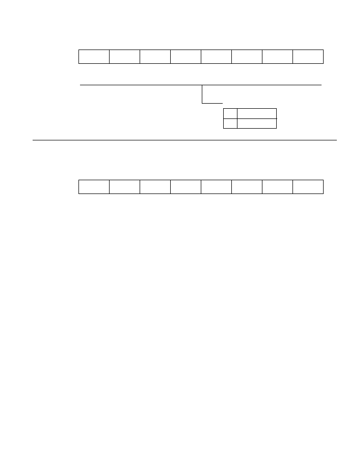
378
P9DDR--Port 9 Data Direction Register
H'FFFE
Port 9
Bit
7
6
5
4
3
2
1
0
P9
7
DDR P9
6
DDR P9
5
DDR P9
4
DDR P9
3
DDR P9
2
DDR P9
1
DDR P9
0
DDR
Initial value
0
0
0
0
0
0
0
0
Read/Write
W
W
W
W
W
W
W
W
P9DR--Port 9 Data Register
H'FFFF
Port 9
Bit
7
6
5
4
3
2
1
0
P9
7
P9
6
P9
5
P9
4
P9
3
P9
2
P9
1
P9
0
Initial value
0
0
0
0
0
0
0
0
Read/Write
R/W
R/W
R/W
R/W
R/W
R/W
R/W
R/W
Port 9 Input/Output Selection
0
Input port
1
Output port

379
TCR--Timer Control Register
H'FF90
FRT1
Bit
7
6
5
4
3
2
1
0
ICIE
OCIEB
OCIEA
OVIE
OEB
OEA
CKS1
CKS0
Initial value
0
0
0
0
0
0
0
0
Read/Write
R/W
R/W
R/W
R/W
R/W
R/W
R/W
R/W
Output Enable A
0
Compare-A output is disabled.
1
Compare-A output is enabled.
Output Enable B
0
Compare-B output is disabled.
1
Compare-B output is enabled.
Timer Overflow Interrupt Enable
0
Overflow interrupt request is disabled.
1
Overflow interrupt request is enabled.
Output Compare Interrupt Enable A
0
Compare-match A interrupt request is disabled.
1
Compare-match A interrupt request is enabled.
Output Compare Interrupt Enable B
0
Compare-match B interrupt request is disabled.
1
Compare-match B interrupt request is enabled.
Input Capture Interrupt Enable
0
Input capture interrupt is disabled.
1
Input capture interrupt is enabled.
Clock Select
00 Internal clock
source: ¯4
01 Internal clock
source: ¯8
10 Internal clock
source: ¯32
11 External clock source:
counted on rising edge
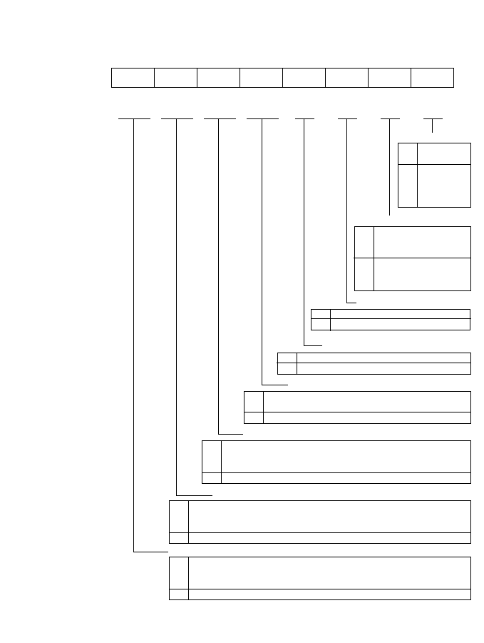
380
TCSR--Timer Control/Status Register
H'FF91
FRT1
Bit
7
6
5
4
3
2
1
0
ICF
OCFB
OCFA
OVF
OLVLB
OLVLA
IEDG
CCLRA
Initial value
0
0
0
0
0
0
0
0
Read/Write
R/(W)
*
R/(W)
*
R/(W)
*
R/(W)
*
R/W
R/W
R/W
R/W
Input Edge Select
0
Count is captured on
falling edge of input
capture signal (FTI).
1
Count is captured on
rising edge of input
capture signal.
Output Level A
0
Compare-match A causes 0 output.
1
Compare-match A causes 1 output.
Output Level B
0
Compare-match B causes 0 output.
1
Compare-match B causes 1 output.
Timer Overflow
0
Cleared from 1 to 0 when CPU reads OVF =
1, then writes 0 in OVF.
1
Set to 1 when FRC changes from H'FFFF to H'0000.
Output Compare Flag A
0
Cleared from 1 to 0 when:
1. CPU reads OCFA = 1, then writes 0 in OCFA.
2. OCIA interrupt is served by DTC.
1
Set to 1 when FRC = OCRA.
Output Compare Flag B
0
Cleared from 1 to 0 when:
1. CPU reads OCFB = 1, then writes 0 in OCFB.
2. OCIB interrupt is served by DTC.
1
Set to 1 when FRC = OCRB.
Input Capture Flag
0
Cleared from 1 to 0 when:
1. CPU reads ICF = 1, then writes 0 in ICF.
2. ICI interrupt is served by DTC.
1
Set to 1 when input capture signal is received and FRC count is copied to ICR.
Counter Clear A
0
FRC count
is not cleared.
1
FRC count is
cleared by
compare-
match A.
*
Only writing of a 0 to
clear the flag is enabled.
381
FRC (H and L)--Free-Running Counter
H'FF92, H'FF93
FRT 1
Bit
7
6
5
4
3
2
1
0
Initial value
0
0
0
0
0
0
0
0
Read/Write
R/W
R/W
R/W
R/W
R/W
R/W
R/W
R/W
Count value
OCRA (H and L)--Output Compare Register A
H'FF94, H'FF95
FRT 1
Bit
7
6
5
4
3
2
1
0
Initial value
1
1
1
1
1
1
1
1
Read/Write
R/W
R/W
R/W
R/W
R/W
R/W
R/W
R/W
Continually compared with FRC. OCFA is set to 1 when OCRA = FRC.
OCRB (H and L)--Output Compare Register B
H'FF96, H'FF97
FRT 1
Bit
7
6
5
4
3
2
1
0
Initial value
1
1
1
1
1
1
1
1
Read/Write
R/W
R/W
R/W
R/W
R/W
R/W
R/W
R/W
Continually compared with FRC. OCFB is set to 1 when OCRB = FRC.
ICR (H and L)--Input Capture Register
H'FF98, H'FF99
FRT 1
Bit
7
6
5
4
3
2
1
0
Initial value
0
0
0
0
0
0
0
0
Read/Write
R
R
R
R
R
R
R
R
Contains FRC count captured when external input capture signal changes.

382
TCR--Timer Control Register
H'FFA0
FRT 2
Bit
7
6
5
4
3
2
1
0
ICIE
OCIEB
OCIEA
OVIE
OEB
OEA
CKS1
CKS0
Initial value
0
0
0
0
0
0
0
0
Read/Write
R/W
R/W
R/W
R/W
R/W
R/W
R/W
R/W
Note: Bit functions are the same as for FRT1.
TCSR--Timer Control/Status Register
H'FFA1
FRT 2
Bit
7
6
5
4
3
2
1
0
ICF
OCFB
OCFA
OVF
OLVLB
OLVLA
IEDG
CCLRA
Initial value
0
0
0
0
0
0
0
0
Read/Write
R/(W)
*
R/(W)
*
R/(W)
*
R/(W)
*
R/W
R/W
R/W
R/W
Note: Bit functions are the same as for FRT1.
*
Only writing of a 0 to clear the flag is enabled.
FRC (H and L)--Free-Running Counter
H'FFA2, H'FFA3
FRT 2
Bit
7
6
5
4
3
2
1
0
Initial value
0
0
0
0
0
0
0
0
Read/Write
R/W
R/W
R/W
R/W
R/W
R/W
R/W
R/W
Note: Bit functions are the same as for FRT1.

OCRA (H and L)--Output Compare Register A
H'FFA4, H'FFA5
FRT 2
Bit
7
6
5
4
3
2
1
0
Initial value
1
1
1
1
1
1
1
1
Read/Write
R/W
R/W
R/W
R/W
R/W
R/W
R/W
R/W
Note: Bit functions are the same as for FRT1.
OCRB (H and L)--Output Compare Register B
H'FFA6, H'FFA7
FRT 2
Bit
7
6
5
4
3
2
1
0
Initial value
1
1
1
1
1
1
1
1
Read/Write
R/W
R/W
R/W
R/W
R/W
R/W
R/W
R/W
Note: Bit functions are the same as for FRT1.
ICR (H and L)--Input Capture Register
H'FFA8, H'FFA9
FRT 2
Bit
7
6
5
4
3
2
1
0
Initial value
0
0
0
0
0
0
0
0
Read/Write
R
R
R
R
R
R
R
R
Note: Bit functions are the same as for FRT1.
TCR--Timer Control Register
H'FFB0
FRT 3
Bit
7
6
5
4
3
2
1
0
ICIE
OCIEB
OCIEA
OVIE
OEB
OEA
CKS1
CKS0
Initial value
0
0
0
0
0
0
0
0
Read/Write
R/W
R/W
R/W
R/W
R/W
R/W
R/W
R/W
Note: Bit functions are the same as for FRT1.
383

TCSR--Timer Control/Status Register
H'FFB1
FRT 3
Bit
7
6
5
4
3
2
1
0
ICF
OCFB
OCFA
OVF
OLVLB
OLVLA
IEDG
CCLRA
Initial value
0
0
0
0
0
0
0
0
Read/Write
R/(W)
*
R/(W)
*
R/(W)
*
R/(W)
*
R/W
R/W
R/W
R/W
Note: Bit functions are the same as for FRT1.
*
Only writing of 0 to clear the flag is enabled.
FRC (H and L)--Free-Running Counter
H'FFB2, H'FFB3
FRT 3
Bit
7
6
5
4
3
2
1
0
Initial value
0
0
0
0
0
0
0
0
Read/Write
R/W
R/W
R/W
R/W
R/W
R/W
R/W
R/W
Note: Bit functions are the same as for FRT1.
OCRA (H and L)--Output Compare Register A
H'FFB4, H'FFB5
FRT 3
Bit
7
6
5
4
3
2
1
0
Initial value
1
1
1
1
1
1
1
1
Read/Write
R/W
R/W
R/W
R/W
R/W
R/W
R/W
R/W
Note: Bit functions are the same as for FRT1.
384

OCRB (H and L)--Output Compare Register B
H'FFB6, H'FFB7
FRT 3
Bit
7
6
5
4
3
2
1
0
Initial value
1
1
1
1
1
1
1
1
Read/Write
R/W
R/W
R/W
R/W
R/W
R/W
R/W
R/W
Note: Bit functions are the same as for FRT1.
ICR (H and L)--Input Capture Register
H'FFB8, H'FFB9
FRT 3
Bit
7
6
5
4
3
2
1
0
Initial value
0
0
0
0
0
0
0
0
Read/Write
R
R
R
R
R
R
R
R
Note: Bit functions are the same as for FRT1.
385
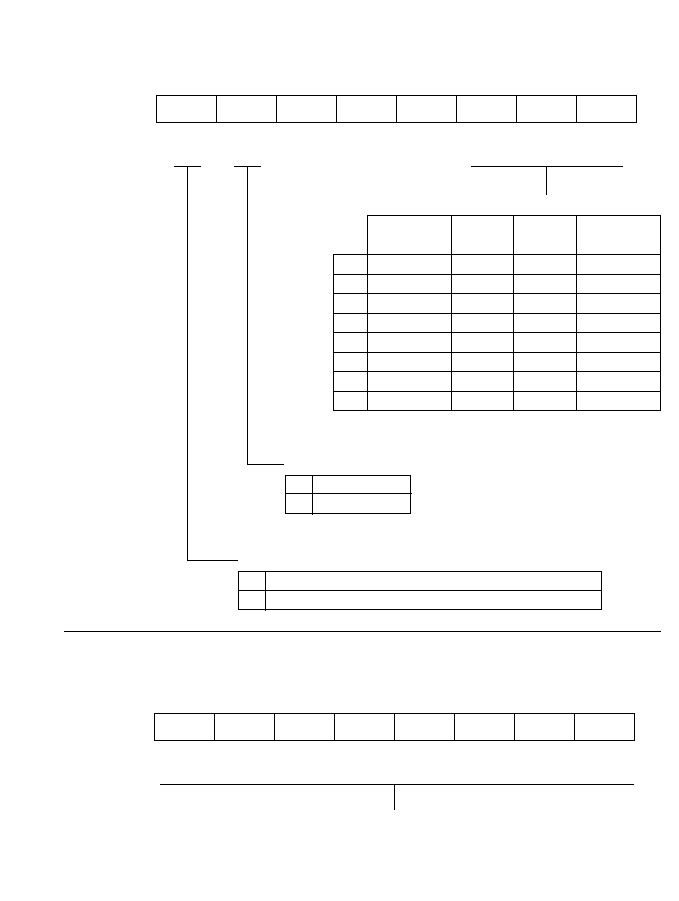
386
TCR--Timer Control Register
H'FFC0
PWM1
Bit
7
6
5
4
3
2
1
0
OE
OS
--
--
--
CKS2
CKS1
CKS0
Initial value
0
0
1
1
1
0
0
0
Read/Write
R/W
R/W
--
--
--
R/W
R/W
R/W
Clock Select (Values When ¯ = 10MHz)
Internal
Reso-
PW
PW
Clock Freq. lution
Period
Frequency
000
¯/2
200ns
50µs
20kHz
001
¯/8
800ns
200µs
5kHz
010
¯/32
3.2µs
800µs
1.25kHz
011
¯/128
12.8µs
3.2ms
312.5kHz
100
¯/256
25.6µs
6.4ms
156.3Hz
101
¯/1024
102.4µs
25.6ms
39.1Hz
110
¯/2048
204.8µs
51.2ms
19.5Hz
111
¯/4096
409.6µs
102.4ms 9.8Hz
Output Enable
0
PW output disabled; TCNT cleared to H'00 and stops.
1
PW output enabled; TCNT runs.
Output Select
0
Positive logic
1
Negative logic
DTR--Duty Register
H'FFC1
PWM1
Bit
7
6
5
4
3
2
1
0
Initial value
1
1
1
1
1
1
1
1
Read/Write
R/W
R/W
R/W
R/W
R/W
R/W
R/W
R/W
Pulse duty factor

387
TCNT--Timer Counter
H'FFC2
PWM1
Bit
7
6
5
4
3
2
1
0
Initial value
0
0
0
0
0
0
0
0
Read/Write
R/(W)
*
R/(W)
*
R/(W)
*
R/(W)
*
R/(W)
*
R/(W)
*
R/(W)
*
R/(W)
*
*
Write function is for test purposes only. Writing to this register during normal operation may have
unpredictable effects
Count value (runs from H'00 to H'F9, then repeats from H'00)
TCR--Timer Control Register
H'FFC4
PWM2
Bit
7
6
5
4
3
2
1
0
OE
OS
--
--
--
CKS2
CKS1
CKS0
Initial value
0
0
1
1
1
0
0
0
Read/Write
R/W
R/W
--
--
--
R/W
R/W
R/W
Note: Bit functions are the same as for PWM1.
DTR--Duty Register
H'FFC5
PWM2
Bit
7
6
5
4
3
2
1
0
Initial value
1
1
1
1
1
1
1
1
Read/Write
R/W
R/W
R/W
R/W
R/W
R/W
R/W
R/W
Note: Bit functions are the same as for PWM1.

388
TCNT--Timer Counter
H'FFC6
PWM2
Bit
7
6
5
4
3
2
1
0
Initial value
0
0
0
0
0
0
0
0
Read/Write
R/(W)
*
R/(W)
*
R/(W)
*
R/(W)
*
R/(W)
*
R/(W)
*
R/(W)
*
R/(W)
*
Note: Bit functions are the same as for PWM1.
*
Write function is for test purposes only. Writing to this register during normal operation may have
unpredictable effects
TCR--Timer Control Register
H'FFC8
PWM3
Bit
7
6
5
4
3
2
1
0
OE
OS
--
--
--
CKS2
CKS1
CKS0
Initial value
0
0
1
1
1
0
0
0
Read/Write
R/W
R/W
--
--
--
R/W
R/W
R/W
Note: Bit functions are the same as for PWM1.
DTR--Duty Register
H'FFC9
PWM3
Bit
7
6
5
4
3
2
1
0
Initial value
1
1
1
1
1
1
1
1
Read/Write
R/W
R/W
R/W
R/W
R/W
R/W
R/W
R/W
Note: Bit functions are the same as for PWM1.

TCNT--Timer Counter
H'FFCA
PWM3
Bit
7
6
5
4
3
2
1
0
Initial value
0
0
0
0
0
0
0
0
Read/Write
R/(W)
*
R/(W)
*
R/(W)
*
R/(W)
*
R/(W)
*
R/(W)
*
R/(W)
*
R/(W)
*
Note: Bit functions are the same as for PWM1.
*
Write function is for test purposes only. Writing to this register during normal operation may have
unpredictable effects.
389
390
TCR--Timer Control Register
H'FFD0
TMR
Bit
7
6
5
4
3
2
1
0
CMIEB
CMIEA
OVIE
CCLR1
CCLR0
CKS2
CKS1
CKS0
Initial value
0
0
0
0
0
0
0
0
Read/Write
R/W
R/W
R/W
R/W
R/W
R/W
R/W
R/W
Counter Clear
0 0 Counter is not cleared.
0 1 Cleared by compare-match A.
1 0 Cleared by compare-match B.
1 1 Cleared on rising edge of external reset input.
Clock Select
0 0 0 No clock source; timer stops.
0 0 1 Internal clock source: ¯8,
counted on falling edge.
0 1 0 Internal clock source: ¯64,
counted on falling edge.
0 1 1 Internal clock source: ¯1024,
counted on falling edge.
1 0 0 No clock source; timer stops.
1 0 1 External clock source, counted
on rising edge.
1 1 0 External clock source, counted
on falling edge.
1 1 1
External clock source, counted
on both rising and falling edges.
Timer Overflow Interrupt Enable
0
Overflow interrupt request is disabled.
1
Overflow interrupt request is enabled.
Compare-Match Interrupt Enable A
0
Compare-match A interrupt request is disabled.
1
Compare-match A interrupt request is enabled.
Compare-Match Interrupt Enable B
0
Compare-match B interrupt request is disabled.
1
Compare-match B interrupt request is enabled.

391
TCSR--Timer Control/Status Register
H'FFD1
TMR
Bit
7
6
5
4
3
2
1
0
CMFB
CMFA
OVF
--
OS3
*
2
OS2
*
2
OS1
*
2
OS0
*
2
Initial value
0
0
0
1
0
0
0
0
Read/Write
R/(W)
*
1
R/(W)
*
1
R/(W)
*
1
--
R/W
R/W
R/W
R/W
Output Select
0 0 No change on compare-match B.
0 1 Output 0 on compare-match B.
1 0 Output 1 on compare-match B.
1 1 Invert (toggle) output on compare-match B.
Output Select
0 0 No change on compare-match A.
0 1 Output 0 on compare-match A.
1 0 Output 1 on compare-match A.
1 1 Invert (toggle) output on compare-match A.
Timer Overflow Flag
0
Cleared from 1 to 0 when CPU reads OVF =
1, then writes 0 in OVF.
1
Set to 1 when TCNT changes from H'FF to H'00.
Compare-Match Flag B
0
Cleared from 1 to 0 when:
1. CPU reads CMFB = 1, then writes 0 in CMFB.
2. CMB interrupt is served by the DTC.
1
Set to 1 when TCNT = TCORB.
*1 Only writing of 0 to clear the flag is enabled.
*2 When all four bits (OS3 to OS0) are cleared to 0, output is disabled.
Compare-Match Flag A
0
Cleared from 1 to 0 when:
1. CPU reads CMFA = 1, then writes 0 in CMFA.
2. CMA interrupt is served by the DTC.
1
Set to 1 when TCNT = TCORA.

392
TCORA--Time Constant Register A
H'FFD2
TMR
Bit
7
6
5
4
3
2
1
0
Initial value
1
1
1
1
1
1
1
1
Read/Write
R/W
R/W
R/W
R/W
R/W
R/W
R/W
R/W
The CMFA bit is set to 1 when TCORA = TCNT.
TCORB--Time Constant Register B
H'FFD3
TMR
Bit
7
6
5
4
3
2
1
0
Initial value
1
1
1
1
1
1
1
1
Read/Write
R/W
R/W
R/W
R/W
R/W
R/W
R/W
R/W
The CMFB bit is set to 1 when TCORB = TCNT.
TCNT--Timer Counter
H'FFD4
TMR
Bit
7
6
5
4
3
2
1
0
Initial value
0
0
0
0
0
0
0
0
Read/Write
R/W
R/W
R/W
R/W
R/W
R/W
R/W
R/W
Count value

393
SMR--Serial Mode Register
H'FFD8
SCI
Bit
7
6
5
4
3
2
1
0
C/A
CHR
PE
O/E
STOP
--
CKS1
CKS0
Initial value
0
0
0
0
0
1
0
0
Read/Write
R/W
R/W
R/W
R/W
R/W
--
R/W
R/W
Stop Bit Length
0
One stop bit
1
Two stop bits
Parity Mode
0
Even parity
1
Odd parity
Character Length
0
8-Bit data length
1
7-Bit data length
Communication Mode
0
Asynchronous
1
Synchronous
Parity Enable
0
Transmit: No parity bit added.
Receive: Parity bit not checked.
1
Transmit: Parity bit added.
Receive: Parity bit checked.
Clock Select
0 0 ¯ clock
0 1 ¯/4 clock
1 0 ¯/16 clock
1 1 ¯/64 clock
BRR--Bit Rate Register
H'FFD9
SCI
Bit
7
6
5
4
3
2
1
0
Initial value
1
1
1
1
1
1
1
1
Read/Write
R/W
R/W
R/W
R/W
R/W
R/W
R/W
R/W
Constant that determines the baud rate
SCR--Serial Control Register
H'FFDA
SCI
Bit
7
6
5
4
3
2
1
0
TIE
RIE
TE
RE
--
--
CKE1
CKE0
Initial value
0
0
0
0
1
1
0
0
Read/Write
R/W
R/W
R/W
R/W
--
--
R/W
R/W
Clock Enable 0
0
SCK pin is NOT USED.
1
SCK pin is used for output.
Clock Enable 1
0
Internal clock
1
External clock, input at SCK pin
Receive Enable
0
Receive disabled
1
Receive enabled
Transmit Enable
0
Transmit disabled
1
Transmit enabled
Receive Interrupt Enable
0
Receive interrupt request (RXI) is disabled.
1
Receive interrupt request (RXI) is enabled.
Transmit Interrupt Enable
0
Transmit interrupt request (TXI) is disabled.
1
Transmit interrupt request (TXI) is enabled.
394

TDR--Transmit Data Register
H'FFDB
SCI
Bit
7
6
5
4
3
2
1
0
Initial value
1
1
1
1
1
1
1
1
Read/Write
R/W
R/W
R/W
R/W
R/W
R/W
R/W
R/W
Transmit data
395
396
SSR--Serial Status Register
H'FFDC
SCI
Bit
7
6
5
4
3
2
1
0
TDRE
RDRF
ORER
FER
PER
--
--
--
Initial value
1
0
0
0
0
1
1
1
Read/Write
R/(W)
*
R/(W)
*
R/(W)
*
R/(W)
*
R/(W)
*
--
--
--
Parity Error
0 Cleared from 1 to 0 when:
1. CPU reads PER = 1, then writes 0 in PER.
2. The chip is reset or enters a standby mode.
1 Set to 1 when a parity error occurs (parity of
receive data does not match parity selected by bit).
Framing Error
0 Cleared from 1 to 0 when:
1. CPU reads FER = 1, then writes 0 in FER.
2. The chip is reset or enters a standby mode.
1 Set to 1 when a framing error occurs (stop bit is 0).
Overrun Error
0 Cleared from 1 to 0 when:
1. CPU reads ORER = 1, then writes 0 in ORER.
2. The chip is reset or enters a standby mode.
1 Set to 1 when an overrun error occurs (next data is
completely received while RDRF bit is set to 1).
Receive Data Register Full
0 Cleared from 1 to 0 when:
1. CPU reads RDRF = 1, then writes 0 in RDRF.
2. RDR is read by the DTC.
3. The chip is reset or enters a standby mode.
1 Set to 1 when one character is received normally and
transferred from RSR to RDR.
* Only writing of 0 to clear the flag is enabled.
Transmit Data Register Empty
0 Cleared from 1 to 0 when:
1. CPU reads TDRE = 1, then writes 0 in TDRE.
2. The DTC writes data in TDR.
1 Set to 1 when:
1. The chip is reset or enters a standby mode.
2. Data is transferred from TDR to TSR.
3. CPU reads TDRE = 0, then clears 0 in TE.

RDR--Receive Data Register
H'FFDD
SCI
Bit
7
6
5
4
3
2
1
0
Initial value
0
0
0
0
0
0
0
0
Read/Write
R
R
R
R
R
R
R
R
Receive data
ADDRn (H)--A/D Data Register n (High)
H'FFE0, H'FFE2, H'FFE4, H'FFE6
(n = A, B, C, D)
A/D
Bit
7
6
5
4
3
2
1
0
AD
9
AD
8
AD
7
AD
6
AD
5
AD
4
AD
3
AD
2
Initial value
0
0
0
0
0
0
0
0
Read/Write
R
R
R
R
R
R
R
R
Upper 8 bits of 10-bit A/D conversion result
ADDRn (L)--A/D Data Register n (Low)
H'FFE1, H'FFE3, H'FFE5, H'FFE7
(n = A, B, C, D)
A/D
Bit
7
6
5
4
3
2
1
0
AD
1
AD
0
--
--
--
--
--
--
Initial value
0
0
0
0
0
0
0
0
Read/Write
R
R
R
R
R
R
R
R
Lower 2 bits of 10-bit A/D conversion result
397
398
ADCSR--A/D Control/Status Register
H'FFE8
A/D
Bit
7
6
5
4
3
2
1
0
ADF
ADIE
ADST
SCAN
CKS
CH2
CH1
CH0
Initial value
0
0
0
0
0
0
0
0
Read/Write
R/(W)
*
R/W
R/W
R/W
R/W
R/W
R/W
R/W
Channel Select
CH2 CH1 CH0
Single Mode
Scan Mode
0
0
AN
0
AN
0
0
1
AN
1
AN
0
, AN
1
1
0
AN
2
AN
0
to AN
2
1
1
AN
3
AN
0
to AN
3
0
0
AN
4
AN
4
0
1
AN
5
AN
4
, AN
5
1
0
AN
6
AN
4
to AN
6
1
1
AN
7
AN
4
to AN
7
0
1
Clock Select
0 Conversion time = 274 states
1 Conversion time = 138 states
Scan Mode
0 Single mode
1 Scan mode
A/D Start
0 A/D conversion is halted.
1 1. Single mode: One A/D conversion is performed,
then this bit is automatically cleared to 0.
2. Scan mode: A/D conversion starts and continues
cyclically on all selected channels until 0 is
written in this bit.
A/D Interrupt Enable
0 The A/D interrupt request (ADI) is disabled.
1 The A/D interrupt request (ADI) is enabled.
* Only writing of 0 to clear the flag is enabled.
A/D End Flag
0 Cleared from 1 to 0 when:
1. The chip is reset or enters a standby mode.
2. CPU reads ADF = 1, then writes 0 in ADF.
3. DTC is served by ADI.
1 Set to 1 at the following times:
1. Single mode: at the completion of A/D conversion.
2. Scan mode: when all selected channels have been converted.
399
TCSR--Timer Status/Control Register
H'FFEC
*1
, H'FFED
*2
WDT
Bit
7
6
5
4
3
2
1
0
OVF
WT/IT
TME
--
--
CKS2
CKS1
CKS0
Initial value
0
0
0
1
1
0
0
0
Read/Write
R/(W)
*3
R/W
R/W
--
--
R/W
R/W
R/W
Timer Enable
0 Timer is disabled.
∑ TCNT is initialized to H'00 and stopped.
1 Timer is enabled.
∑ TCNT starts incrementing.
∑ CPU interrupt request is enabled.
Timer Mode Select
0 Interval timer mode (IRQ
0
interrupt request)
1 Watchdog timer mode (NMI interrupt request)
*1 Read address
*2 Write address
*3 Only writing of 0 to clear the flag is enabled.
*4 Times in parentheses are the times for TCNT to increment from H'00 to H'FF and change to
H'00 again when ¯ = 10MHz.
Overflow Flag
0 Cleared from 1 to 0 when CPU reads OVF = 1, then wtites 0
in OVF.
1 Set to 1 when TCNT changes from H'FF to H'00.
Clock Select
0 0 0 ¯/2
(51.2µs)
*4
0 0 1 ¯/32
(819.2µs)
0 1 0 ¯/64
(1.6ms)
0 1 1 ¯/128
(3.3ms)
1 0 0 ¯/256
(6.6ms)
1 0 1 ¯/512
(13.1ms)
1 1 0 ¯/2048
(52.4ms)
1 1 1 ¯/4096
(104.9ms)
TCNT--Timer Counter
H'FFED
WDT
Bit
7
6
5
4
3
2
1
0
Initial value
0
0
0
0
0
0
0
0
Read/Write
R/W
R/W
R/W
R/W
R/W
R/W
R/W
R/W
Count value
IPRA--Interrupt Priority Register A
H'FFF0
INTC
Bit
7
6
5
4
3
2
1
0
--
--
Initial value
0
0
0
0
0
0
0
0
Read/Write
R
R/W
R/W
R/W
R
R/W
R/W
R/W
IRQ
0
interrupt priority level (0 to 7)
IRQ
1
interrupt priority level (0 to 7)
IPRB--Interrupt Priority Register B
H'FFF1
INTC
Bit
7
6
5
4
3
2
1
0
--
--
Initial value
0
0
0
0
0
0
0
0
Read/Write
R
R/W
R/W
R/W
R
R/W
R/W
R/W
16-Bit FRT1 interrupt
priority level (0 to 7)
16-Bit FRT2 interrupt
priority level (0 to 7)
400

IPRC--Interrupt Priority Register C
H'FFF2
INTC
Bit
7
6
5
4
3
2
1
0
--
--
Initial value
0
0
0
0
0
0
0
0
Read/Write
R
R/W
R/W
R/W
R
R/W
R/W
R/W
8-Bit timer interrupt
priority level (0 to 7)
16-Bit FRT3 interrupt
priority level (0 to 7)
IPRD--Interrupt Priority Register D
H'FFF3
INTC
Bit
7
6
5
4
3
2
1
0
--
--
Initial value
0
0
0
0
0
0
0
0
Read/Write
R
R/W
R/W
R/W
R
R/W
R/W
R/W
A/D interrupt priority
level (0 to 7)
SCI interrupt priority
level (0 to 7)
IPRD--Interrupt Priority Register D
H'FFF4
INTC
Bit
7
6
5
4
3
2
1
0
--
--
--
--
--
--
Initial value
0
0
0
0
0
0
0
0
Read/Write
R/W
R/W
R/W
R/W
R/W
R/W
R/W
R/W
IRQ
0
0 Served by CPU
1 Served by DTC
IRQ
1
0 Served by CPU
1 Served by DTC
401

DTEB--Data Transfer Enable Register B
H'FFF5
INTC
Bit
7
6
5
4
3
2
1
0
--
--
Initial value
0
0
0
0
0
0
0
0
Read/Write
R/W
R/W
R/W
R/W
R/W
R/W
R/W
R/W
ICI
0 Served by CPU
1 Served by DTC
OCIA
0 Served by CPU
1 Served by DTC
OCIB
0 Served by CPU
1 Served by DTC
16-Bit FRT channel 1
16-Bit FRT channel 2
ICI
0 Served by CPU
1 Served by DTC
OCIA
0 Served by CPU
1 Served by DTC
OCIB
0 Served by CPU
1 Served by DTC
402

DTEC--Data Transfer Enable Register C
H'FFF6
INTC
Bit
7
6
5
4
3
2
1
0
--
--
--
Initial value
0
0
0
0
0
0
0
0
Read/Write
R/W
R/W
R/W
R/W
R/W
R/W
R/W
R/W
ICI
0 Served by CPU
1 Served by DTC
OCIA
0 Served by CPU
1 Served by DTC
OCIB
0 Served by CPU
1 Served by DTC
16-Bit FRT channel 3
8-Bit timer
CMIA
0 Served by CPU
1 Served by DTC
CMIB
0 Served by CPU
1 Served by DTC
403
DTED--Data Transfer Enable Register D
H'FFF7
INTC
Bit
7
6
5
4
3
2
1
0
--
--
--
--
--
Initial value
0
0
0
0
0
0
0
0
Read/Write
R/W
R/W
R/W
R/W
R/W
R/W
R/W
R/W
RXI
0 Served by CPU
1 Served by DTC
TXI
0 Served by CPU
1 Served by DTC
SCI
A/D converter
ADI
0 Served by CPU
1 Served by DTC
404
WCR--Wait-State Control Register
H'FFF8
WSC
Bit
7
6
5
4
3
2
1
0
--
--
--
--
WMS1
WMS0
WC1
WC0
Initial value
1
1
1
1
0
0
1
1
Read/Write
--
--
--
--
R/W
R/W
R/W
R/W
Wait Count 1 and 0
0 0 No wait states (T
W
)
are inserted.
0 1 1 Wait states are inserted.
1 0 2 Wait states are inserted.
1 1 3 Wait state is inserted.
Wait Mode Select 1 and 0
0 0 Programmable wait mode
0 1 No wait states are inserted,
regardless of the wait count.
1 0 Pin wait mode
1 1 Pin auto-wait mode
RAMCR--RAM Control Register
H'FFF9
RAM
Bit
7
6
5
4
3
2
1
0
RAME
--
--
--
--
--
--
--
Initial value
1
1
1
1
1
1
1
1
Read/Write
R/W
--
--
--
--
--
--
--
RAM Enable
0 On-chip RAM is disabled.
1 On-chip RAM is enabled.
405

MDCR--Mode Control Register
H'FFFA
Bit
7
6
5
4
3
2
1
0
--
--
--
--
--
MDS2
MDS1
MDS0
Initial value
1
1
0
0
0
--
*
--
*
--
*
Read/Write
--
--
--
--
--
R
R
R
Mode Select
Value input at mode pins
* Initialized according to the inputs at pins MD
2
, MD
1
, and MD
0
.
SBYCR--Software Standby Control Register
H'FFFB
Bit
7
6
5
4
3
2
1
0
SSBY
--
--
--
--
--
--
--
Initial value
0
1
1
1
1
1
1
1
Read/Write
R/W
--
--
--
--
--
--
--
Software Standby
0 SLEEP instruction causes transition to sleep mode.
1 SLEEP instruction causes transition to software standby mode.
406

Appendix C I/O Port Schematic Diagrams
C.1 Schematic Diagram of Port 1
Figure C-1 (a) to (g) gives a schematic view of the port 1 input/output circuits.
Table C-1 (a) Port 1 Port Read (Pin P1
0
)
Setting
Port Read Data
DDR = 0
Pin value
DDR = 1
¯
C
R
Q
D
P1 DDR
0
WP1D
Reset
WP1D:
RP1:
Write to P1DDR
Read Port 1
Internal data bus (PDB8)
P1
0
¯
RP1
C
R
Q
D
P1 DDR
1
WP1D
Reset
WP1D:
RP1:
Write to P1DDR
Read Port 1
Internal data bus (PDB9)
P1
1
E
RP1
Figure C-1 (a) Schematic Diagram of Port 1, Pin P1
0
Figure C-1 (b) Schematic Diagram of Port 1, Pin P1
1
407
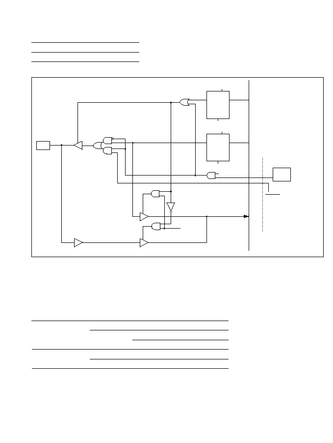
Table C-1 (b) Port 1 Port Read (Pin P1
1
)
Setting
Port Read Data
DDR = 0
Pin value
DDR = 1
E
Table C-1 (c) Port 1 Port Read (Pin P1
2
)
Mode
Setting
Port Read Data
BRLE = 1
DR value
1,2,3,4
BRLE
DDR = 0
Pin value
= 0
DDR = 1
DR value
DDR = 0
Pin value
DDR = 1
DR value
RP1
BRLE
BACK
Q
Port 1 control
register, bit 3
Mode 1, 2, 3,
or 4
WP1
C
R
Q
D
P1 DR
2
C
R
Q
D
P1 DDR
2
WP1D
Reset
Reset
WP1D:
WP1:
RP1:
Write to P1DDR
Write to Port 1
Read Port 1
Internal data bus (PDB10)
P1
2
7
Figure C-1 (c) Schematic Diagram of Port 1, Pin P1
2
408
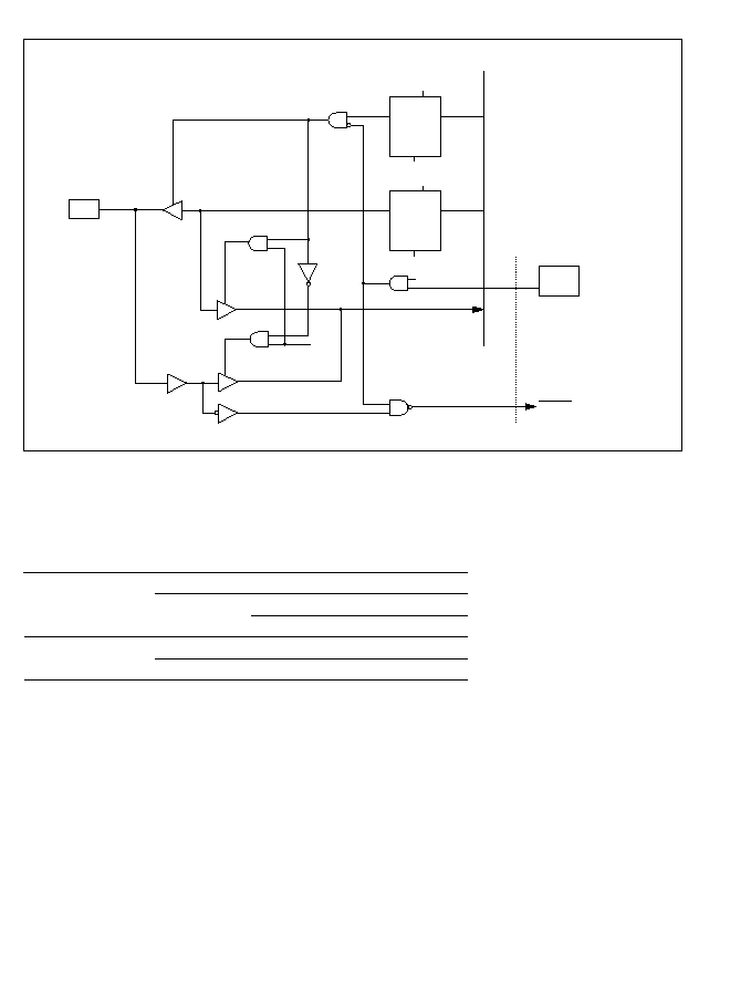
Table C-1 (d) Port 1 Port Read (Pin P1
3
)
Mode
Setting
Port Read Data
BRLE = 1
Pin value
1,2,3,4
BRLE
DDR = 0
Pin value
= 0
DDR = 1
DR value
DDR = 0
Pin value
DDR = 1
DR value
RP1
BREQ to CPU
P1
3
BRLE
Q
Port 1 control register,
bit 3
Mode 1, 2, 3,
or 4
WP1
C
R
Q
D
P1 DR
3
C
R
Q
D
P1 DDR
3
Reset
Reset
WP1D:
WP1:
RP1:
Write to P1DDR
Write to Port 1
Read Port 1
Internal data bus (PDB11)
WP1D
7
Figure C-1 (d) Schematic Diagram of Port 1, Pin P1
3
409
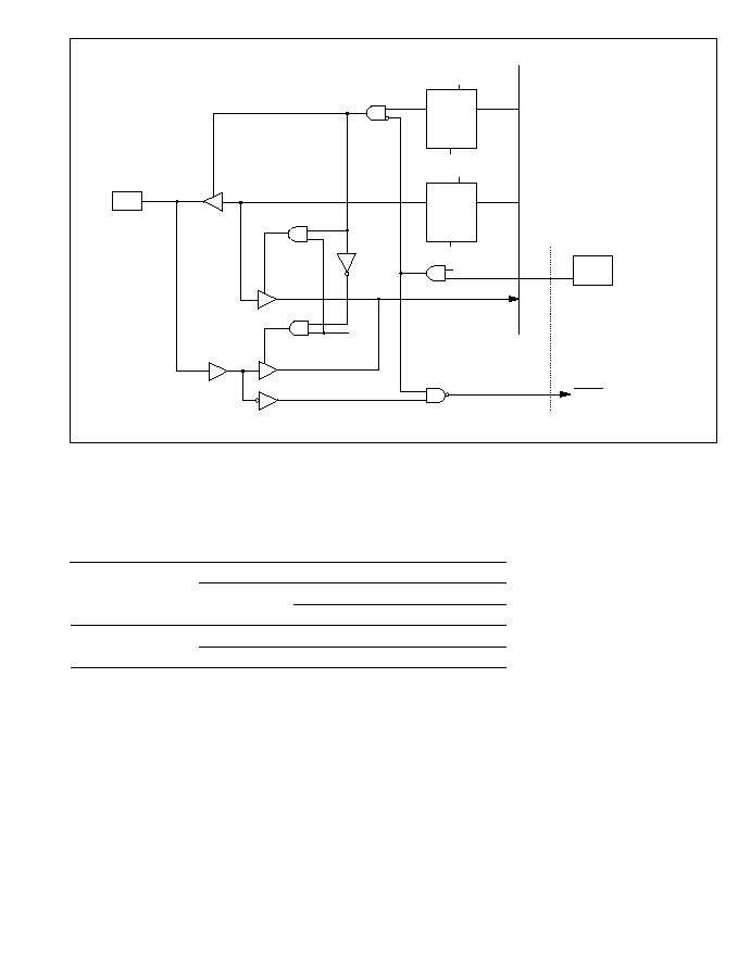
Table C-1 (e) Port 1 Port Read (Pin P1
4
)
Mode
Setting
Port Read Data
WMS 1 = 1
Pin value
1,2,3,4
WMS 1
DDR = 0
Pin value
= 0
DDR = 1
DR value
DDR = 0
Pin value
DDR = 1
DR value
RP1
WAIT to CPU
P1
4
WMS1
Q
Wait-state control
register, bit 3
Mode 1, 2, 3,
or 4
WP1
C
R
Q
D
P1 DR
4
C
R
Q
D
P1 DDR
4
Reset
Reset
WP1D:
WP1:
RP1:
Write to P1DDR
Write to Port 1
Read Port 1
Internal data bus (PDB12)
WP1D
7
Figure C-1 (e) Schematic Diagram of Port 1, Pin P1
4
410
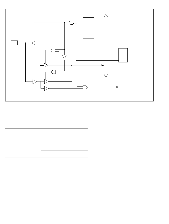
Table C-1 (f) Port 1 Port Read (Pins P1
5
, P1
6
)
Setting
Port Read Data
IRQ
0
E
or
= 1
Pin value
IRQ
1
E
IRQ
0
E
DDR = 0
Pin value
or
= 0
IRQ
1
E
DDR = 1
DR value
RP1
IRQ , IRQ to CPU
P1
n
IRQ E
or
IRQ E
Q
Port 1 control register,
bits 5 and 6
WP1
C
R
Q
D
P1 DR
n
C
R
Q
D
P1 DDR
n
Reset
Reset
WP1D:
WP1:
RP1:
n:
Write to P1DDR
Write to Port 1
Read Port 1
5 or 6
Internal data bus (PDB13, PDB14)
WP1D
0
1
0
1
Figure C-1 (f) Schematic Diagram of Port 1, Pins P1
5
and P1
6
411

Table C-1 (g) Port 1 Port Read (Pin P1
7
)
Setting
Port Read Data
8-bit timer output enable
8-bit timer output value
8-bit timer
DDR = 0
Pin value
output disable
DDR = 1
DR value
RP1
P1
7
WP1
8-Bit timer module
Output enable
8-Bit timer output
WP1D:
WP1:
RP1:
Write to P1DDR
Write to Port 1
Read Port 1
Internal data bus (PDB15)
C
R
Q
D
P1 DR
7
C
R
Q
D
P1 DDR
7
Reset
Reset
WP1D
Figure C-1 (g) Schematic Diagram of Port 1, Pin P1
7
412

C.2 Schematic Diagram of Port 2
Figure C-2 gives a schematic view of the port 2 input/output circuits.
Table C-2 Port 2 Port Read
Mode
Port Read Data
1,2,3,4
DR value
DDR = 0
Pin value
DDR = 1
DR value
WP2D:
WP2:
RP2:
n:
Write to P2DDR
Write to Port 2
Read Port 2
0, 1, 2, 3, or 4
Internal data bus (PDB8 to PDB11)
Mode 1, 2, 3, or 4
Software standby
Bus release
Mode 7
Mode 1, 2, 3, or 4
RP2
Bus control signals
P2
n
WP2
C
R
Q
D
P2 DR
n
C
R
Q
D
P2 DDR
n
Reset
WP2D
Reset
S
7
Figure C-2 Schematic Diagram of Port 2
413
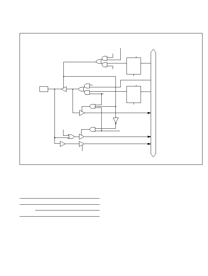
C.3 Schematic Diagram of Port 3
Figure C-3 gives a schematic view of the port 3 input/output circuits.
Table C-3 Port 3 Port Read
Mode
Port Read Data
1,2,3,4
Always reads 1
DDR = 0
Pin value
DDR = 1
DR value
Internal data bus (PDB8 to PDB15)
WP3D:
WP3:
RP3:
n:
Write to P3DDR
Write to Port 3
Read Port 3
0 to 7
WP3D
C
R
Q
D
P3 DR
n
C
R
Q
D
P3 DDR
n
Reset
WP3
Reset
Data bus control
External address read
Mode 7
RP3
Mode 7
Mode 1, 2, 3, or 4
Mode 1, 2, 3, or 4
Mode 1, 2, 3,
or 4
P3
n
7
Figure C-3 Schematic Diagram of Port 3
414

C.4 Schematic Diagram of Port 4
Figure C-4 gives a schematic view of the port 4 input/output circuits.
Table C-4 Port 4 Port Read
Mode
Port Read Data
1,2,3,4
DR value
DDR = 0
Pin value
DDR = 1
DR value
WP4D:
WP4:
RP4:
n:
Write to P4DDR
Write to Port 4
Read Port 4
0 to 7
Internal data bus (PDB8 to PDB15)
Mode 1, 2, 3, or 4
Software standby
Bus release
Mode 7
Mode 1, 2, 3, or 4
RP4
P4
n
WP4
C
R
Q
D
P4 DR
n
C
R
Q
D
P4 DDR
n
Reset
WP4D
Reset
S
Internal address bus (IAB0 to IAB7)
7
Figure C-4 Schematic Diagram of Port 4
415
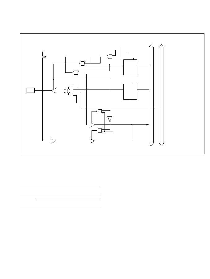
C.5 Schematic Diagram of Port 5
Figure C-5 gives a schematic view of the port 5 input/output circuits.
Table C-5 Port 5 Port Read
Mode
Port Read Data
1,3
DR value
DDR = 0
Pin value
DDR = 1
DR value
WP5D:
WP5:
RP5:
n:
Write to P5DDR
Write to Port 5
Read Port 5
0 to 7
Internal data bus (PDB8 to PDB15)
Mode 1 or 3
Software standby
Bus release
Mode 7
Mode 1, 2, 3, or 4
RP5
P5
n
WP5
C
R
Q
D
P5 DR
n
C
R
Q
D
P5 DDR
n
Reset
WP5D
Reset
S
Internal address bus (IAB8 to IAB15)
MOS
pull-up
Mode 1, 2, 3, or 4
2,4,7
Figure C-5 Schematic Diagram of Port 5
416
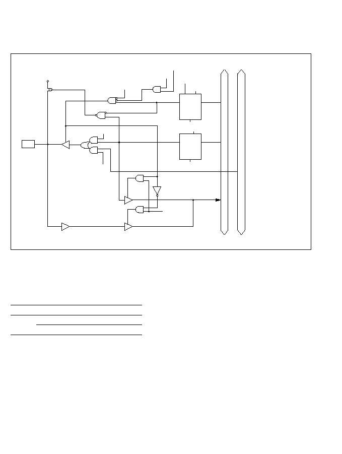
C.6 Schematic Diagram of Port 6
Figure C-6 gives a schematic view of the port 6 input/output circuits.
Table C-6 Port 6 Port Read
Mode
Port Read Data
3
DR value
DDR = 0
Pin value
DDR = 1
DR value
WP6D:
WP6:
RP6:
n:
Write to P6DDR
Write to Port 6
Read Port 6
0 to 3
Internal data bus (PDB8 to PDB15)
Mode 3
Software standby
Bus release
Mode 1, 2, or 7
Mode 3 or 4
RP6
P6
n
WP6
C
R
Q
D
P6 DR
n
C
R
Q
D
P6 DDR
n
Reset
WP6D
Reset
S
Internal address bus (IAB16 to IAB19)
MOS
pull-up
Mode 3 or 4
1,2,4,7
Figure C-6 Schematic Diagram of Port 6
417
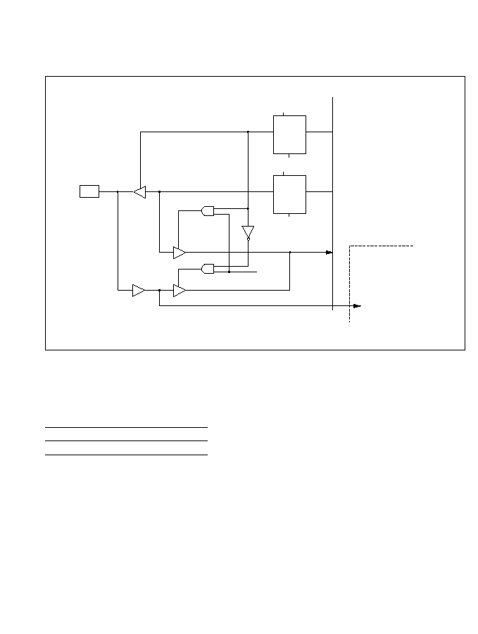
C.7 Schematic Diagram of Port 7
Figure C-7 (a) to (e) gives a schematic view of the port 7 input/output circuits.
Table C-7 (a) Port 7 Port Read (Pin P70)
Setting
Port Read Data
DDR = 0
Pin value
DDR = 1
DR value
RP7
P7
0
WP7
8-Bit timer module
Input clock
WP7D:
WP7:
RP7:
Write to P7DDR
Write to Port 7
Read Port 7
Internal data bus (PDB8)
C
R
Q
D
P7 DR
0
C
R1
Q
D
P7 DDR
0
Reset
Reset
WP7D
Figure C-7 (a) Schematic Diagram of Port 7, Pin P7
0
418
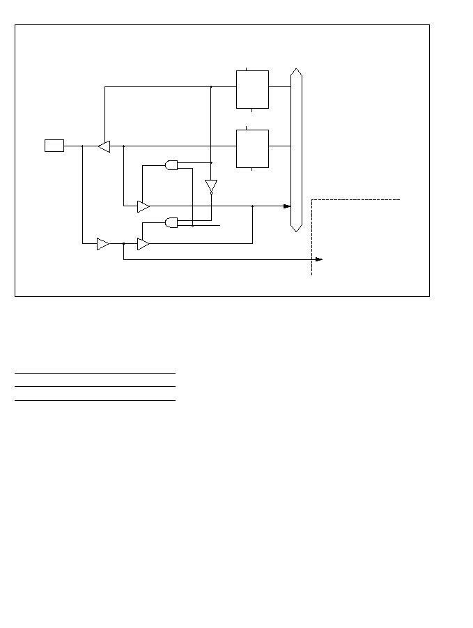
Table C-7 (b) Port 7 Port Read (Pins P7
1
, P7
2
)
Setting
Port Read Data
DDR = 0
Pin value
DDR = 1
DR value
RP7
P7
n
WP7
Free-running timer module
Input capture signal
WP7D:
WP7:
RP7:
n:
Write to P7DDR
Write to Port 7
Read Port 7
1 or 2
Internal data bus (PDB9 to 10)
C
R
Q
D
P7 DR
n
C
R1
Q
D
P7 DDR
n
Reset
Reset
WP7D
Figure C-7 (b) Schematic Diagram of Port 7, Pins P7
1
and P7
2
419
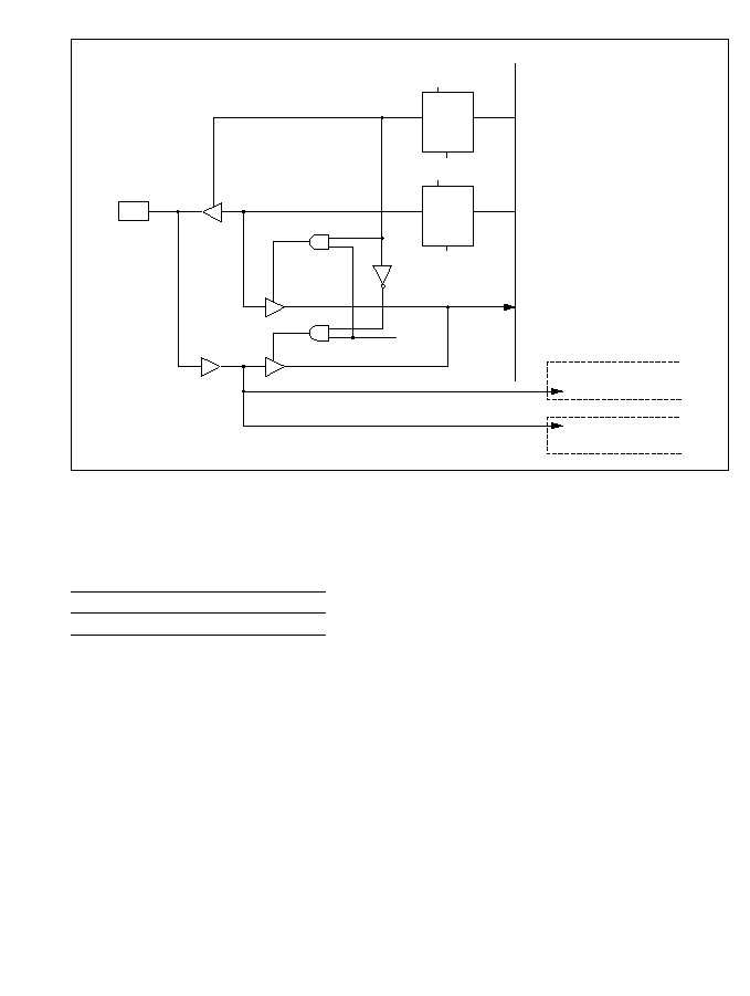
Table C-7 (c) Port 7 Port Read (Pin P7
3
)
Setting
Port Read Data
DDR = 0
Pin value
DDR = 1
DR value
RP7
P7
3
WP7
8-Bit timer module
Counter reset input
WP7D:
WP7:
RP7:
Write to P7DDR
Write to Port 7
Read Port 7
Internal data bus (PDB11)
C
R
Q
D
P7 DR
3
C
R1
Q
D
P7 DDR
3
Reset
Reset
WP7D
Free-running timer module
Input capture signal
Figure C-7 (c) Schematic Diagram of Port 7, Pin P7
3
420
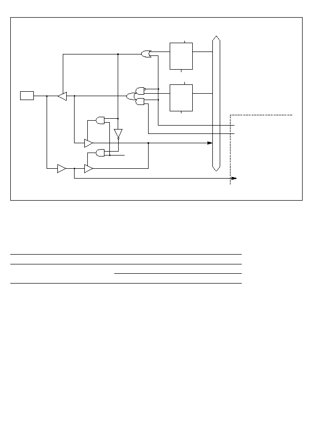
Table C-7 (d) Port 7 Port Read (Pins P7
4
≠ P7
6
)
Setting
Port Read Data
Output enable
Output compare output value
DDR = 0
Pin value
DDR = 1
DR value
RP7
P7
n
WP7
Free-running timer module
Output enable
Output compare output
WP7D:
WP7:
RP7:
n:
Write to P7DDR
Write to Port 7
Read Port 7
4, 5 or 6
Internal data bus (PDB12 to PDB14)
C
R
Q
D
P7 DR
n
C
R
Q
D
P7 DDR
n
Reset
Reset
WP7D
Counter clock output
Output disable
Figure C-7 (d) Schematic Diagram of Port 7, Pins P7
4
, P7
5
and P7
6
421

Table C-7 (e) Port 7 Port Read (Pin P7
7
)
Setting
Port Read Data
Output enable
Output compare output value
DDR = 0
Pin value
DDR = 1
DR value
RP7
P7
7
WP7
Free-running timer module
Output enable
Output compare output
WP7D:
WP7:
RP7:
Write to P7DDR
Write to Port 7
Read Port 7
Internal data bus (PDB15)
C
R
Q
D
P7 DR
7
C
R1
Q
D
P7 DDR
7
Reset
Reset
WP7D
Output disable
Figure C-7 (e) Schematic Diagram of Port 7, Pin P7
7
422

C.8 Schematic Diagram of Port 8
Figure C-8 gives a schematic view of the port 8 input circuits.
P8
n
RP8
RP8:
n:
Read Port 8
0 to 7
A/D converter module
Input multiplexer
Internal data bus
(PDB8 to PDB15)
Figure C-8 Schematic Diagram of Port 8
423
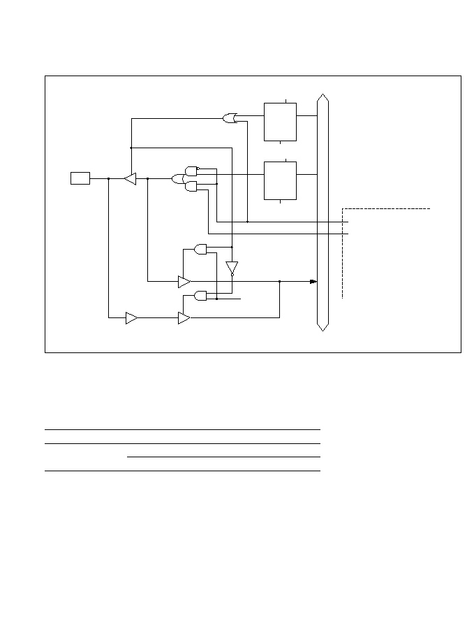
C.9 Schematic Diagram of Port 9
Figure C-9 (a) to (e) gives a schematic view of the port 9 input/output circuits.
Table C-9 (a) Port 9 Port Read (Pins P9
0
, P9
1
)
Setting
Port Read Data
Output enable
Output compare output value
DDR = 0
Pin value
DDR = 1
DR value
RP9
P9
n
WP9
Free-running timer module
Output enable
Output compare output
WP9D:
WP9:
RP9:
n:
Write to P9DDR
Write to Port 9
Read Port 9
0 or 1
Internal data bus (PDB8, PDB9)
C
R
Q
D
P9 DR
n
C
R
Q
D
P9 DDR
n
Reset
Reset
WP9D
Output disable
Figure C-9 (a) Schematic Diagram of Port 9, Pins P9
0
and P9
1
424
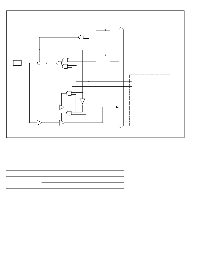
Table C-9 (b) Port 9 Port Read (Pins P9
2
≠ P9
4
)
Setting
Port Read Data
Output enable
PWM 1, 2, 3 output value
DDR = 0
Pin value
DDR = 1
DR value
RP9
P9
n
WP9
PWM timer module
Output enable
PWM , PWM , or PWM output
WP9D:
WP9:
RP9:
n:
Write to P9DDR
Write to Port 9
Read Port 9
2, 3, or 4
Internal data bus (PDB10 to PDB12)
C
R
Q
D
P9 DR
n
C
R
Q
D
P9 DDR
n
Reset
Reset
WP9D
1
2
3
Output disable
Figure C-9 (b) Schematic Diagram of Port 9, Pins P9
2
, P9
3
and P9
4
425
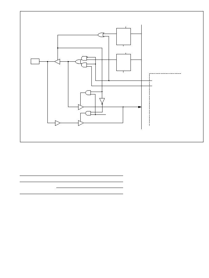
Table C-9 (c) Port 9 Port Read (Pin P9
5
)
Setting
Port Read Data
Output enable
Serial transfer data
DDR = 0
Pin value
DDR = 1
DR value
RP9
P9
5
WP9
SCI timer module
Output enable
Serial transfer data
WP9D:
WP9:
RP9:
Write to P9DDR
Write to Port 9
Read Port 9
Internal data bus (PDB13)
C
R
Q
D
P9 DR
5
C
R
Q
D
P9 DDR
5
Reset
Reset
WP9D
Output disable
Figure C-9 (c) Schematic Diagram of Port 9, Pin P9
5
426
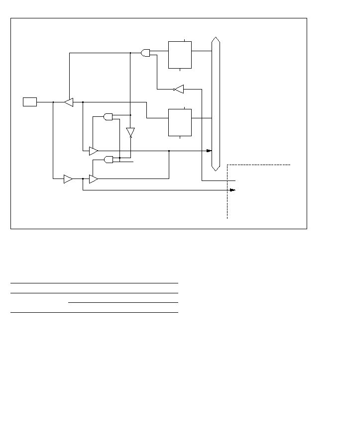
Table C-9 (d) Port 9 Port Read (Pin P9
6
)
Setting
Port Read Data
Output enable
Serial transfer data
DDR = 0
Pin value
DDR = 1
DR value
RP9
P9
6
Fig. C-9 (d)
WP9
SCI timer module
Input enable
WP9D:
WP9:
RP9:
Write to P9DDR
Write to Port 9
Read Port 9
Internal data bus (PDB14)
C
R
Q
D
P9 DR
6
C
R
Q
D
P9 DDR
6
Reset
Reset
WP9D
Serial receive data
Output disable
Figure C-9 (d) Schematic Diagram of Port 9, Pin P9
6
427
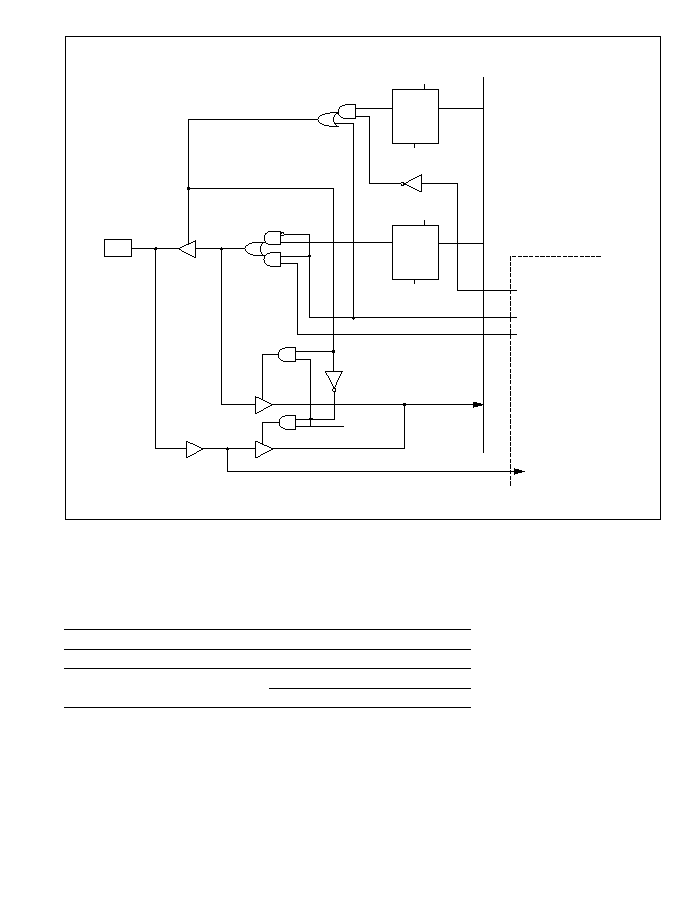
Table C-9 (e) Port 9 Port Read (Pin P9
7
)
Setting
Port Read Data
Clock input enable
Input clock value
Clock output enable
Output clock value
Clock input/output
DDR = 0
Pin value
enable
DDR = 1
DR value
RP9
P9
7
WP9
SCI timer module
Clock input enable
WP9D:
WP9:
RP9:
Write to P9DDR
Write to Port 9
Read Port 9
Internal data bus (PDB15)
C
R
Q
D
P9 DR
7
C
R
Q
D
P9 DDR
7
Reset
Reset
WP9D
Clock output enable
Clock output
Clock input
Figure C-9 (e) Schematic Diagram of Port 9, Pin P9
7
428

429
Appendix D Memory Map
Expanded maxim
um mode
Expanded maxim
um mode
Single-c
hip mode
Mode 1
Mode 2
Mode 3
Mode 4
Mode 7
V
ector tab
les
Exter
nal
memor
y
On-chip RAM
1K b
yte
Register field
128 b
ytes
V
ector tab
les
On-chip R
O
M
32K b
ytes
Exter
nal
memor
y
On-chip RAM
1K b
yte
Register field
128 b
ytes
V
ector tab
les
Exter
nal
memor
y
On-chip RAM
1K b
yte
Register field
128 b
ytes
Exter
nal
memor
y
V
ector tab
les
On-chip R
O
M
32K b
ytes
Exter
nal
memor
y
On-chip RAM
1K b
yte
Register field
128 b
ytes
Exter
nal
memor
y
V
ector tab
les
On-chip R
O
M
32K b
ytes
H'0000
H'00BF
H'00C0
H'FB7F
H'FB80
H'FF7F
H'FF80
H'FFFF
H'0000
H'00BF
H'00C0
H'7FFF
H'8000
P
age 0
H'FB7F
H'FB80
H'FF7F
H'FF80
H'FFFF
H'00000
H'0017F
H'00180
P
age 0
H'0FB7F
H'0FB80
H'0FF7F
H'0FF80
H'0FFFF
H'10000
H'1FFFF
H'F0000
H'FFFFF
H'00000
H'0017F
H'00180
H'07FFF
H'08000
P
age 0
H'0FB7F
H'0FB80
H'0FF7F
H'0FB80
H'0FFFF
H'10000
P
age 1
H'1FFFF
H'F0000
P
age 15
H'FFFFF
H'0000
H'00BF
H'00C0
H'7FFF
P
age 0
H'FB80
H'FF7F
H'FF80
H'FFFF
P
age 1
P
age 15
P
age 0
On-chip RAM
1K b
yte
Register field
128 b
ytes
430
Appendix E Pin State
E.1 Port State of Each Pin State
Table E-1 Port State
Hardware
Port
Standby Software
Bus-right
Program
Execution
Pin Name
Mode Reset
Mode
Standby mode Sleep Mode
Release Mode State (Normal Operation)
P1
7
to P1
2
1
Input/Output port or
TMO, IRQ
1
, IRQ
0
2
Control signal Input/
WAIT, BREQ,
3
T
T
keep
*
1
keep
*
3
keep
*
4
Output
BACK
4
7
keep
*
2
keep
---
Input/Output port
P1
1
/E
1
(DDR = 1)
(DDR = 1)
(DDR = 1)
(DDR = 1)
P1
0
/¯
2
Clock
¯ = H
Clock output
Clock output
Clock output
3
output
T
E = L
(DDR = 0)
(DDR = 0)
(DDR = 0)
4
(DDR = 0)
T
T
Input port
7
T
---
P2
4
to P2
0
1
WR, RD, DS,
WR, RD, DS,
2
H
T
H
T
R/W, AS
R/W, AS
3
4
7
T
keep
keep
---
Input/Output port
P3
7
to P3
0
1
D
7
to D
0
2
T
T
T
D
7
to D
0
3
T
T
4
7
keep
keep
---
Input/Output port
P4
7
to P4
0
1
A
7
to A
0
2
L
T
L
T
A
7
to A
0
3
T
4
7
T
keep
keep
---
Input/Output port
P5
7
to P5
0
1
L
T
L
T'
A
15
to A
8
A
15
to A
8
2
T
T
*
6
*
5
T
*
6
Address/Input port
3
L
T
T
L
T
A
15
to A
8
4
T
T
*
6
*
5
T
*
6
Address/Input port
7
keep
keep
---
Input/Output port
431
Table E-1 Port State (cont)
Hardware
Port
Standby Software
Bus-right
Program
Execution
Pin Name
Mode Reset
Mode
Standby mode Sleep Mode
Release Mode State (Normal Operation)
P6
3
to P6
0
1
A
19
to A
16
2
T
3
L
T
T
L
T
A
19
to A
16
4
T
T
*
6
*
5
T
*
6
Address/Input port
7
keep
keep
---
Input/Output port
P7
7
to P7
0
1
2
3
T
T
keep
*
2
keep
keep
Input port
4
7
P8
7
to P8
0
1
2
3
T
T
T
T
T
Input port
4
7
P9
7
to P9
0
1
2
3
T
T
keep
*
2
keep
keep
Input/Output port
4
7
H: "High" = High level
L: "Low" = Low level
T: High Impedance
keep: If DDR = 0 and DR = 1 in port 5 and 6, Pull-up MOS holds on-state.
Notes:
*
1 8 Bit Timer is reset, so P1
7
becomes input or output port controlled by DDR and DR. Also P1
2
goes to the high impedance state when it is programmed as BACK output.
*
2 On-chip supporting modules are reset. So these pins become input or output ports controlled
by DDR and DR.
*
3 BREQ can be accepted and BACK goes LOW.
*
4 BACK outputs LOW.
*
5 The pins programmed as address bus output LOW and others programmed as input are at the
high impedance state.
If DDR = 0 and DR = 1, the pull-up MOS's keep ON state.
*
6 If DDR = 0 and DR = 1, the pull-up MOS's keep ON state.
keep
keep
keep
Input/Output port
432

Table E-2 Pull-Up MOS State
Port
Mode
Reset
Hardware Standby Mode
Other Operating State
*
P5
7
to P5
0
1
OFF
OFF
OFF
A
15
to A
8
2
ON/OFF
3
OFF
4
ON/OFF
7
P5
7
to P5
0
1
OFF
OFF
ON/OFF
A
15
to A
8
2
3
OFF
4
ON/OFF
7
OFF: Pull-up MOS is always OFF.
ON/OFF: Pull-up MOS holds on-state only when DDR = "0" and DR = 1.
*
Including Software Standby Mode
433

E.2 Pin Status in the Reset State
1. Mode 1
Figures E-1 and E-2 show how the pin states change when the RES pin goes Low during external
memory access in mode 1.
As soon as RES goes Low, all ports are initialized to the input (high-impedance) state. The AS,
DS, RD, and WR signals all go High. The data bus (D
7
to D
0
) is placed in the high-impedance
state.
The address bus and the R/W signal are initialized 1.5 ¯ clock periods after the Low state of the
RES pin is sampled. All address bus signals are made Low. The R/W signal is made High.
The clock output pins P1
0
/¯ and P1
1
/E are initialized 0.5 ¯ clock periods after the Low state of the
RES pin is sampled. Both pins are initialized to the output state.
434

ZTAT Versions
A to A
15
0
RES
P1 / ¯*
0
Internal reset signal
R/W
AS, RD and DS (read)
WR and DS (write)
D to D (write)
7
0
I/O ports
High impedance
High impedance
H'0000
External memory access
T
1
T
2
T
3
*
The dotted line indicates that P1
0
/¯ is an input port if the corresponding DDR bit is 0,
but a clock output pin if the DDR bit is 1.
Figure E-1 Reset during Memory Access (Mode 1)
435
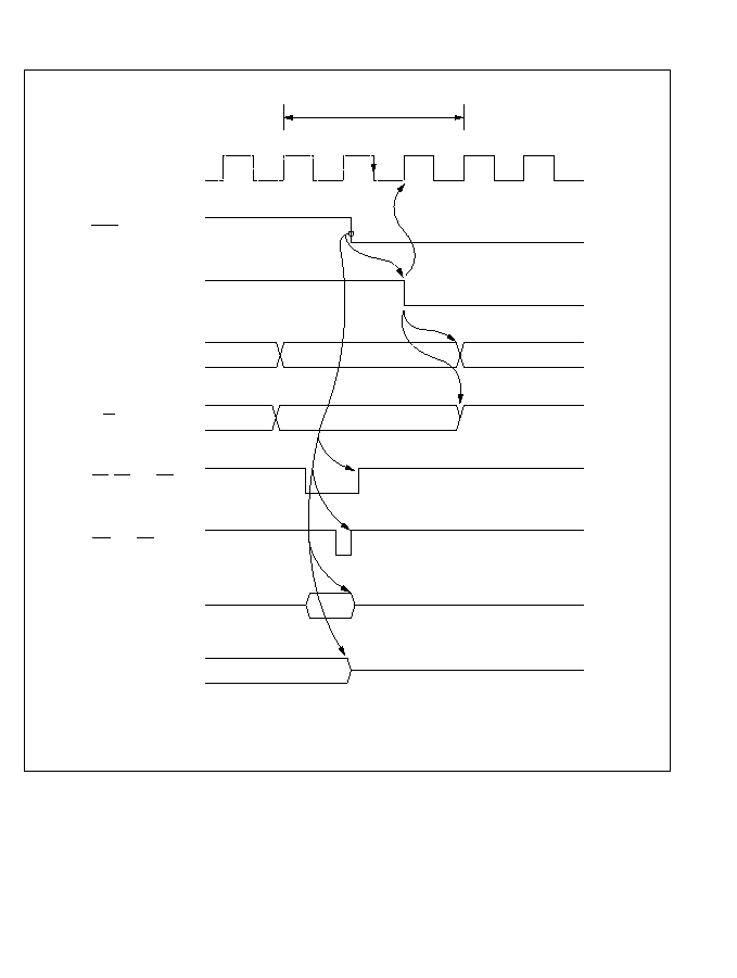
Masked-ROM Versions
Figure E-2 Reset during Memory Access (Mode 1)
A to A
15
0
RES
P1 / ¯*
0
Internal reset signal
R/W
AS, RD and DS (read)
WR and DS (write)
D to D (write)
7
0
I/O ports
High impedance
High impedance
H'0000
External memory access
T
1
T
2
T
3
*
The dotted line indicates that P1
0
/¯ is an input port if the corresponding DDR bit is 0,
but a clock output pin if the DDR bit is 1.
436

2. Mode 2
Figures E-3 and E-4 show how the pin states change when the RES pin goes Low during external
memory access in mode 2.
As soon as RES goes Low, all ports are initialized to the input (high-impedance) state. The AS,
DS, RD, and WR signals all go High. The data bus (D
7
to D
0
) is placed in the high-impedance
state. Pins P5
7
/A
15
to P5
0
/A
8
of the address bus are initialized as input ports.
Pins A
7
to A
0
of the address bus and the R/W signal are initialized 1.5 ¯ clock periods after the
Low state of the RES pin is sampled. Pins A
7
to A
0
are made Low. The signal is made High.
The clock output pins P1
0
/¯ and P1
1
/E are initialized 0.5 ¯ clock periods after the Low state of the
RES pin is sampled. Both pins are initialized to the output state.
437

ZTAT Versions
High impedance
H'00
T
1
T
2
T
3
External memory access
High impedance
High impedance
RES
P1 / ¯*
0
Internal reset signal
R/W
AS, RD and DS (read)
WR and DS (write)
D to D (write)
7
0
I/O ports
A to A
7
0
P5 /A to P5 to A
7
15
0
8
*
The dotted line indicates that P1
0
/¯ is an input port if the corresponding DDR bit is 0,
but a clock output pin if the DDR bit is 1.
Figure E-3 Reset during Memory Access (Mode 2)
438
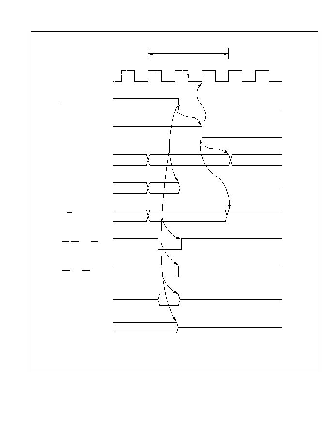
Masked-ROM Versions
A to A
7
0
RES
P1 / ¯*
0
Internal reset signal
R/W
AS, RD and DS (read)
WR and DS (write)
D to D (write)
7
0
I/O ports
High impedance
High impedance
H'00
External memory access
T
1
T
2
T
3
P5 /A to P5 /A
7
15
0
8
High impedance
*
The dotted line indicates that P1
0
/¯ is an input port if the corresponding DDR bit is 0,
but a clock output pin if the DDR bit is 1.
Figure E-4 Reset during Memory Access (Mode 2)
439

3. Mode 3
Figures E-5 and E-6 show how the pin states change when the RES pin goes Low during external
memory access in mode 3.
As soon as RES goes Low, all ports are initialized to the input (high-impedance) state. The AS,
DS, RD, and WR signals all go High. The data bus (D
7
to D
0
) is placed in the high-impedance
state.
The address bus and the signal are initialized 1.5 ¯ clock periods after the Low state of the RES
pin is sampled. All address bus signals are made Low. The R/W signal is made High.
The clock output pins P1
0
/¯ and P1
1
/E are initialized 0.5 ¯ clock periods after the Low state of the
RES pin is sampled. Both pins are initialized to the output state.
440
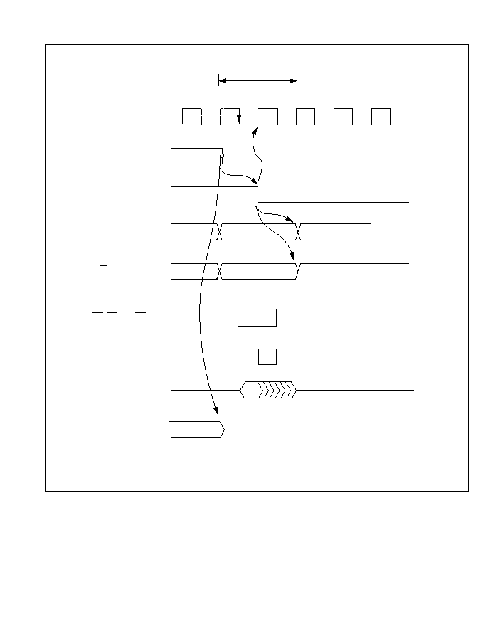
ZTAT Version
High impedance
High impedance
H'00000
T
1
T
2
External memory
access
A to A
19
0
RES
P1 / ¯*
0
Internal reset signal
R/W
AS, RD and DS (read)
WR and DS (write)
D to D (write)
7
0
I/O ports
*
The dotted line indicates that P1
0
/¯ is an input port if the corresponding DDR bit is 0,
but a clock output pin if the DDR bit is 1.
Figure E-5 Reset during Memory Access (Mode 3)
441
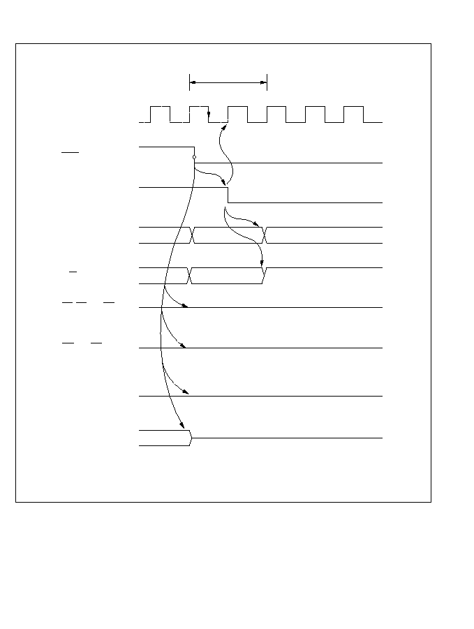
Masked-ROM Version
A to A
19
0
RES
P1 / ¯*
0
Internal reset signal
R/W
AS, RD and DS (read)
WR and DS (write)
D to D (write)
7
0
I/O ports
High impedance
H'0000
External memory access
T
1
T
2
High impedance
*
The dotted line indicates that P1
0
/¯ is an input port if the corresponding DDR bit is 0,
but a clock output pin if the DDR bit is 1.
Figure E-6 Reset during Memory Access (Mode 3)
442

4. Mode 4
Figures E-7 and E-8 show how the pin states change when the RES pin goes Low during external
memory access in mode 4.
As soon as RES goes Low, all ports are initialized to the input (high-impedance) state. The AS,
DS, RD, and WR signals all go High. The data bus (D
7
to D
0
) is placed in the high-impedance
state. Pins P5
7
/A
15
to P5
0
/A
8
of the address bus and pins P6
3
/A
19
to P6
0
/A
16
of the page address
bus are initialized as input ports.
Pins A
7
to A
0
of the address bus and the R/W signal are initialized 1.5 ¯ clock periods after the
Low state of the RES pin is sampled. Pins A
7
to A
0
are made Low. The R/W signal is made
High.
The clock output pins P1
0
/¯ and P1
1
/E are initialized 0.5 ¯ clock periods after the Low state of the
RES pin is sampled. Both pins are initialized to the output state.
443
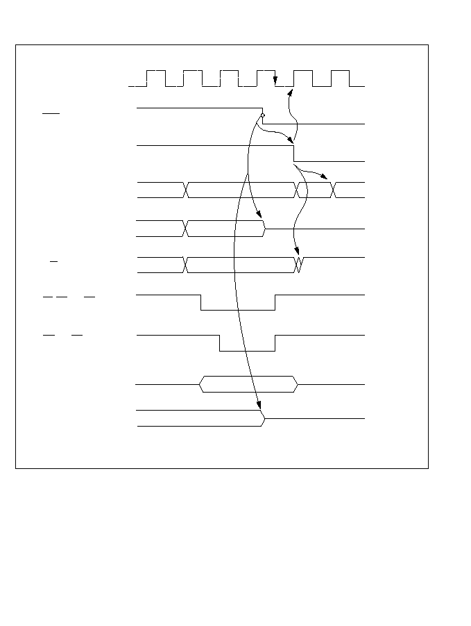
ZTAT Versions
T
1
T
2
T
3
T
1
H'00
High impedance
High impedance
High impedance
RES
P1 / ¯*
0
Internal reset signal
R/W
AS, RD and DS (read)
WR and DS (write)
D to D (write)
7
0
I/O ports
A to A
7
0
P6 /A to P6 to A and
3
19
0
16
P5 /A to P5 /A
7
15
0
8
*
The dotted line indicates that P1
0
/¯ is an input port if the corresponding DDR bit is 0,
but a clock output pin if the DDR bit is 1.
Figure E-7 Reset during Memory Access (Mode 4)
444
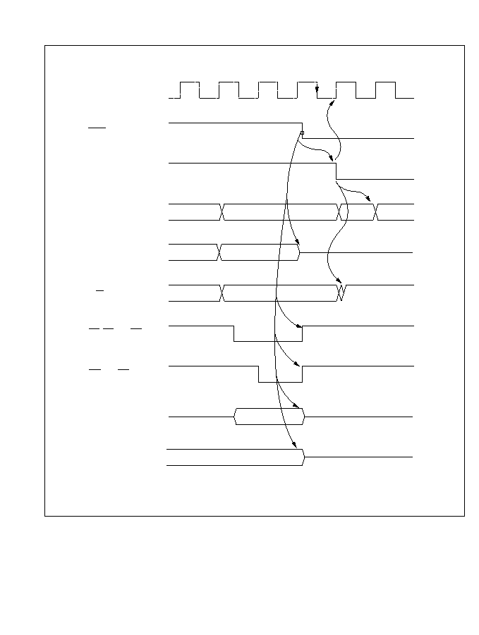
Masked-ROM Versions
A to A
7
0
RES
P1 / ¯*
0
Internal reset signal
R/W
AS, RD and DS (read)
WR and DS (write)
D to D (write)
7
0
I/O ports
High impedance
H'00
T
1
T
2
T
3
T
1
High impedance
High impedance
P6 /A to P6 /A ,
P5 /A to P5 /A
3
19
0
16
7
15
0
8
*
The dotted line indicates that P1
0
/¯ is an input port if the corresponding DDR bit is 0,
but a clock output pin if the DDR bit is 1.
Figure E-8 Reset during Memory Access (Mode 4)
445
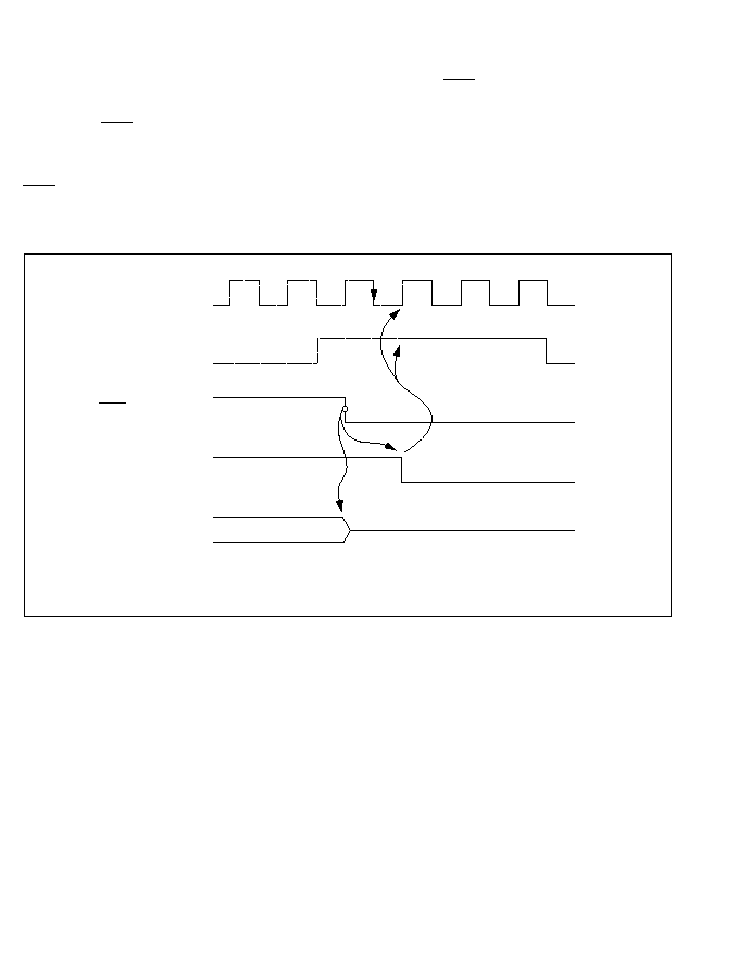
5. Mode 7
Figures E-9 and E-10 show how the pin states change when the RES pin goes Low in mode 7.
As soon as RES goes Low, all ports are initialized to the input (high-impedance) state.
The clock output pins P1
0
/¯ and P1
1
/E are initialized 0.5 ¯ clock periods after the Low state of the
RES pin is sampled. Both pins are initialized to the output state.
ZTAT Versions
High impedance
RES
P1 / ¯*
0
Internal reset signal
I/O ports
P1 / E*
0
*
The dotted line indicates that P1
0
/¯ and P1
0
/E are input port if the corresponding DDR
bit is 0, but clock output pins if the DDR bit is 1.
Figure E-9 Reset during Memory Access (Mode 7)
446

Masked-ROM Versions
RES
P1 / ¯*
0
Internal reset signal
I/O ports
High impedance
P1 /E*
0
*
The dotted line indicates that P1
0
/¯ and P1
0
/E are input port if the corresponding DDR
bit is 0, but clock output pins if the DDR bit is 1.
Figure E-10 Reset during Memory Access (Mode 7)
447

Appendix F Timing of Entry to and Recovery from
Hardware Standby Mode
Timing of Entry to Hardware Standby Mode
(1) To preserve RAM contents, drive the RES signal line low 10 system clock cycles before the
fall of the STBY signal.
The RES signal can rise any time after STBY goes low. The minimum necessary time from
STBY low to RES high is 0 ns.
(2) When it is not necessary to preserve RAM contents, RES need not be driven low as in (1).
Timing of Exit from Hardware Standby Mode
Drive the RES signal line low approximately 100 ns before the rise of the STBY signal.
RES
STBY
t
1
t
2
RES
STBY
t = 100ns
t
OSC
449

Appendix G Package Dimensions
Figure G-1 shows the dimensions of the CP-84 package. Figure G-2 shows the dimensions of the
CG-84 package. Figure G-3 shows the dimensions of the FP-80A package.
Figure G-1 Package Dimensions (CP-84)
Figure G-2 Package Dimensions (CG-84)
451

Figure G-3 Package Dimensions (FP-80A)
452