Preliminary
Rev. 1.1E '99.02.10
HD66421
(RAM-Provided 160 Channel 4-Level Grey Scale Driver
for Dot Matrix Graphics LCD)
Description
The HD66421 drives and controls a dot matrix
graphic LCD(Liquid Crystal Display) using a
bit-mapped method. It provides a highly
flexible display through its on-chip display
RAM, in which each two bits of data can be
used to turn on or off one dot on LCD panel
with four-level grey scale.
A single HD66421 can display a maximum of
160x100 dots using its powerful display
control functions. It can display only eight
lines out of one hundred lines.
This function realize low power consumption
because high voltage for driving LCD is not
needed.
An MPU can access HD66421 at any time,
because the MPU operations are asynchronous
with the HD66421's system clock and display
operation.
Its low-voltage operation at 2.2 to 5.5V and
standby function provides low power
-dissipation, making the HD66421 suitable for
small portable device applications.
Features
∑ Built-in bit-mapped display RAM: 30kbits
(160 x 100 x 2 bits)
∑ Grey scale display: PWM four-level grey
scale can be selected from 32 levels
∑ Grey scale memory management: Packed
pixel
∑ Monochrome display: two planes can be
selected. One plane is displayed while the other
plane is being written.
∑ Partial display: Eight-lines data can be
displayed in any place
∑ An 80-system MPU interface
∑ Power supply voltage for operation : 2.2V to
5.5V
∑ Power supply voltage for LCD : 18 V max.
∑ Selectable multiplex duty ratio: 1/8, 1/64, 1/80,
1/100
∑ LCD driving alternating cycle: 7, 11, 13 lines
or flame
∑ Built-in oscillator: external resister
∑ Low power consumption:
∑ Circuits for generating LCD driving voltage :
Contrast control, Operational amplifier, and
Resistive dividers
∑ Internal resistive divider: programmable bias
rate
∑ 32-level programmable contrast control
∑ Wide range of instructions
reversible display, display on/off, vertical
display scroll, blink, reversible address,
read-modify-write mode
∑ Package: TCP
Type No.
HD66421TB0
HCD66421BP
Package
TCP
Die with gold bump
Ordering Information
HD66421
1
Preliminary
Rev. 1.1E '99.02.10
HD66421
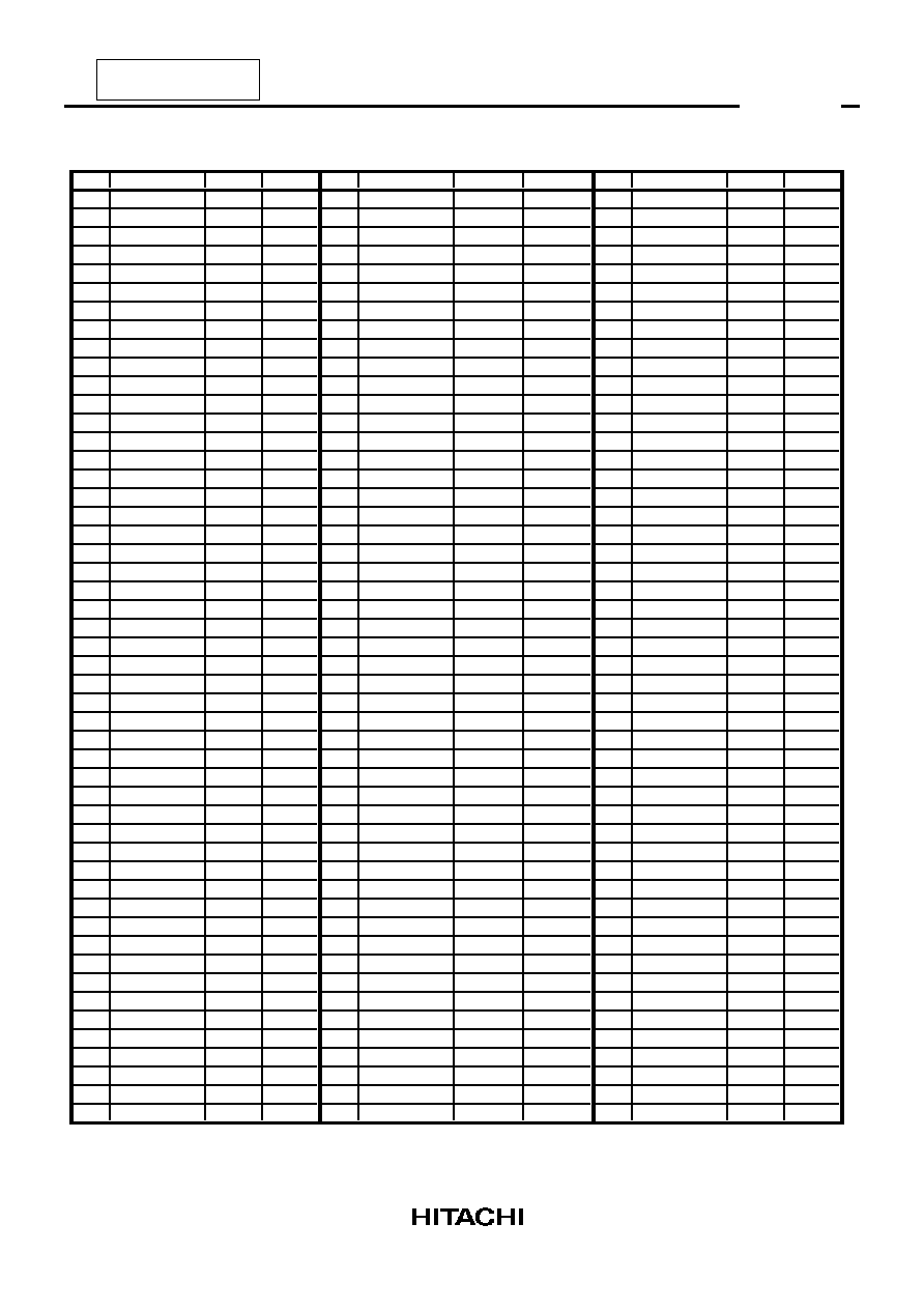
Pad Location Coordinate
No.
PAD NAME
X
Y
No.
PAD NAME
X
Y
No.
PAD NAME
X
Y
1
COM1
-4217
1731
31
COM31
-4217
230
61
SEG11
-4217
-1299
2
COM2
-4217
1681
32
COM32
-4217
179
62
SEG12
-4217
-1349
3
COM3
-4217
1631
33
COM33
-4217
129
63
SEG13
-4217
-1399
4
COM4
-4217
1581
34
COM34
-4217
79
64
SEG14
-4217
-1449
5
COM5
-4217
1531
35
COM35
-4217
29
65
SEG15
-4217
-1499
6
COM6
-4217
1481
36
COM36
-4217
-21
66
SEG16
-4217
-1549
7
COM7
-4217
1430
37
COM37
-4217
-71
67
SEG17
-4217
-1599
8
COM8
-4217
1380
38
COM38
-4217
-121
68
SEG18
-4217
-1649
9
COM9
-4217
1330
39
COM39
-4217
-171
69
SEG19
-4217
-1699
10
COM10
-4217
1280
40
COM40
-4217
-221
70
SEG20
-4217
-1749
11
COM11
-4217
1230
41
COM41
-4217
-271
71
SEG21
-4217
-1799
12
COM12
-4217
1180
42
COM42
-4217
-321
72
SEG22
-4217
-1849
13
COM13
-4217
1130
43
COM43
-4217
-371
73
SEG23
-4217
-1899
14
COM14
-4217
1080
44
COM44
-4217
-421
74
SEG24
-4217
-1949
15
COM15
-4217
1030
45
COM45
-4217
-471
75
dummy A
-4217
-2082
16
COM16
-4217
980
46
COM46
-4217
-521
76
dummy 1
-4029
-2082
17
COM17
-4217
930
47
COM47
-4217
-571
77
dummy 2
-3907
-2082
18
COM18
-4217
880
48
COM48
-4217
-621
78
dummy 3
-3827
-2082
19
COM19
-4217
830
49
COM49
-4217
-671
79
dummy 4
-3619
-2082
20
COM20
-4217
780
50
COM50
-4217
-721
80
dummy 5
-3497
-2075
21
COM21
-4217
730
51
SEG1
-4217
-798
81
dummy 6
-3419
-2075
22
COM22
-4217
680
52
SEG2
-4217
-848
82
SEG25
-2822
-2082
23
COM23
-4217
630
53
SEG3
-4217
-898
83
SEG26
-2772
-2082
24
COM24
-4217
580
54
SEG4
-4217
-948
84
SEG27
-2722
-2082
25
COM25
-4217
530
55
SEG5
-4217
-998
85
SEG28
-2672
-2082
26
COM26
-4217
480
56
SEG6
-4217
-1049
86
SEG29
-2622
-2082
27
COM27
-4217
430
57
SEG7
-4217
-1099
87
SEG30
-2572
-2082
28
COM28
-4217
380
58
SEG8
-4217
-1149
88
SEG31
-2522
-2082
29
COM29
-4217
330
59
SEG9
-4217
-1199
89
SEG32
-2472
-2082
30
COM30
-4217
280
60
SEG10
-4217
-1249
90
SEG33
-2422
-2082
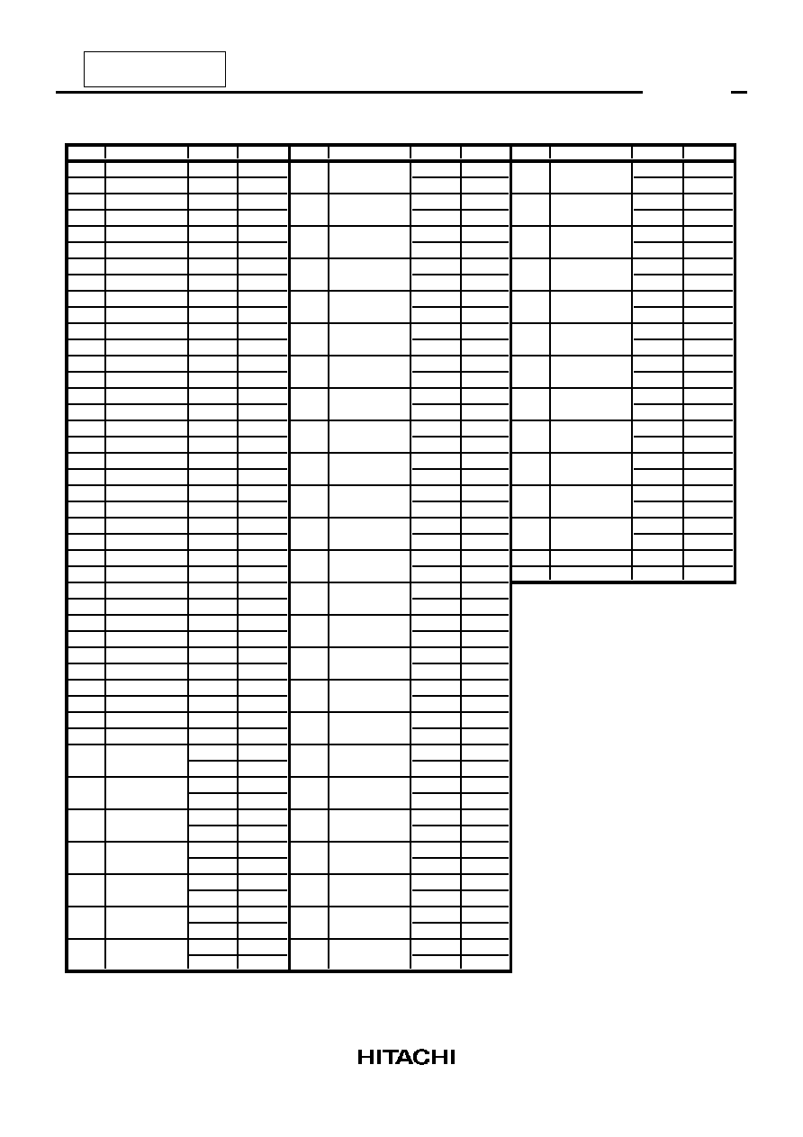
GND7
COM1
SEG24
dummyA
dummy1
GND8
dummy12
dummy8
SEG137
COM100
GND1
GND2
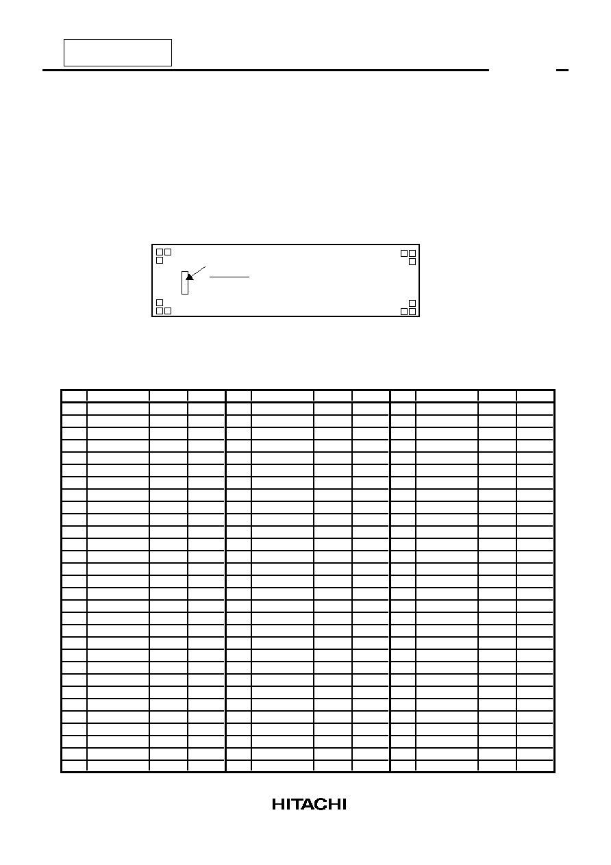
Type code
HD66421
Pad Arrangement
Chip size : 8.99 x 4.72 mm
Coordinate : Pad center
Origin : Chip Center
Bump size : GND1, GND8, dummy A, dummy B 70 x 70 µm
Power, I/O (Pad No. 276 to 321) 50 x 70 µm
COM1 - 100, SEG1 - 160, dummy1 -12 35 x 50 µm
3