
364
HD66712U
(Dot-Matrix Liquid Crystal Display Controller/Driver)
Description
The HD66712 dot-matrix liquid crystal display controller and driver LSI displays alphanumerics,
numbers, and symbols. It can be configured to drive a dot-matrix liquid crystal display under the control
of a serial or a 4- or 8-bit microprocessor. Since all the functions such as display RAM, character
generator, and liquid crystal driver, required for driving a dot-matrix liquid crystal display are internally
provided on one chip, a minimum system can be interfaced with this controller/driver.
A single HD66712 is capable of displaying a single 24-character line, two 24-character lines, or four 12-
character lines.
The HD66712 software is upwardly compatible with the LCDII (HD44780) which allows the user to
easily replace an LCD-II with an HD66712. In addition, the HD66712 is equipped with functions such as
segment displays for icon marks, a 4-line display mode, and a horizontal smooth scroll, and thus supports
various display forms. This achieves various display forms. The HD66712 character generator ROM is
extended to generate 240 5
◊
8 dot characters.
The low-voltage operation (2.7V) of the HD66712, combined with a low-power mode, is suitable for any
portable battery-driven product requiring low power consumption.
Features
∑
5
◊
8 dot matrix possible
∑
Clock-synchronized serial interface capability; can interface with 4- or 8-bit MPU
∑
Low-power operation support:
2.7 to 5.5V (low voltage)
Wide liquid-crystal voltage range: 2.7 to 11.0V max.
∑
Booster for liquid crystal voltage
Two/three times (13V max.)
∑
High-speed MPU bus interface
(2MHz at 5-V operation)

HD66712U
365
∑
Extension driver interface
∑
Character display and independent 60-icon mark display possible
∑
Horizontal smooth scroll by 6-dot font width display possible
∑
80
◊
8-bit display RAM (80 characters max.)
∑
9,600-bit character generator ROM
240 characters (5
◊
8 dot)
∑
64
◊
8-bit character generator RAM
8 characters (5
◊
8 dot)
∑
16
◊
8-bit segment icon mark
96-segment icon mark
∑
34-common
◊
60-segment liquid crystal display driver
∑
Programmable duty cycle
(See List 1)
∑
Software upwardly compatible with HD44780
∑
Wide range of instruction functions:
Functions compatible with LCD-II: Display clear, cursor home, display on/off, cursor on/off,
display character blink, cursor shift, display shift
Additional functions: Icon mark control, 4-line display, horizontal smooth scroll, 6-dot character
width control, white-black inverting blinking cursor
∑
Automatic reset circuit that initializes the controller/driver after power on (standard version only)
∑
Internal oscillator with an external resistor
∑
Low power consumption
∑
TCP-128 pin, bare-chip
List 1 Programmable Duty Cycles
Number
5-Dot Font Width
6-Dot Font Width
of Lines
Duty Ratio
Displayed Characters
Icons
Displayed Characters
Icons
1
1/17
One 24-character
line
60
One 20-character
lines
60
2
1/33
Two 24-character
lines
60
Two 20-character
lines
60
3
1/33
Four 12-character
lines
60
Four 10-character
lines
60
HD66712U
366
Ordering Information
Type No.
Package
CGROM
HD66712SA00FS
QFP1420-128 (FP-128)
Japanese standard
HD66712SA01FS
QFP1420-128 (FP-128)
Communication
HD66712SA02FS
QFP1420-128 (FP-128)
European font
HCD66712UA02
Chip
HD66712UA02TA0
Standard TCP-128
HD66712UA03TA0
Standard TCP-128
Japanese + European font
HCD66712UA03
Chip
HCD66712UA03BP
Chip with bump

HD66712U
367
LCD-II Family Comparison
Item
HD66702
HD66710
HD66712S
HD66712U
Power supply voltage
5V ±10 %
(standard)
2.7V to 5.5V
(low voltage)
2.7V to 5.5V
2.7V to 5.5V
Liquid crystal drive
voltage
3.0V to 8.3V
3.0V to 13.0V
3.0V to 13.0V
2.7V to 11.0V
Maximum display digits
per chip
20 characters
◊
2 lines
16 characters
◊
2 lines/
8 characters
◊
4 lines
24 characters
◊
2 lines/
12 characters
◊
4 lines
Segment display
None
40 segments
60 segments
Display duty cycle
1/8, 1/11, and 1/16 1/17 and 1/33
1/17 and 1/33
CGROM
7,200 bits
(160 5
◊
7 dot
characters and 32
5
◊
10 dot
characters)
9,600 bits
(240 5
◊
8 dot
characters)
9,600 bits
(240 5
◊
8 dot
characters)
CGRAM
64 bytes
64 bytes
64 bytes
DDRAM
80 bytes
80 bytes
80 bytes
SEGRAM
None
8 bytes
16 bytes
Segment signals
100
40
60
Common signals
16
33
34
Liquid crystal drive
waveform
B
B
B
Bleeder resistor for LCD
power supply
External
(adjustable)
External
(adjustable)
External
(adjustable)
Clock source
External resistor or
external clock
External resistor or
external clock
External resistor or
external clock
R
f
oscillation frequency
(frame frequency)
320 kHz ±30%
(70 to 130 Hz for
1/8 and 1/16 duty
cycle; 51 to 95 Hz
for 1/11 duty cycle)
270 kHz ±30%
(56 to 103 Hz for
1/17 duty cycle;
57 to 106 Hz for
1/33 duty cycle)
270 kHz ±30%
(56 to 103 Hz for
1/17 duty cycle;
57 to 106 Hz for
1/33 duty cycle)
R
f
resistance
68 k
: 5-V
operation;
56 k
: (3-V
operation)
91 k
: 5-V
operation;
75 k
: 3-V
operation
91 k
: 5-V
operation;
75 k
: 3-V
operation
130 k
: 5-V
operation
110 k
: 3-V
operation

HD66712U
368
Item
HD66702
HD66710
HD66712S
HD66712U
Liquid crystal voltage
booster circuit
None
2-3 times step-up
circuit
2-3 times step-up
circuit
Extension driver control
signal
Independent
control signal
Used in common
with a driver output
pin
Independent control
signal
Reset function
Power on automatic
reset
Power on automatic
reset
Power on automatic
reset or Reset input
Instructions
Fully compatible
with the LCD-II
Uppercompatible
with the LCD-II
Upper compatible
with the LCD-II
Number of displayed
lines
1 or 2
1, 2, or 4
1, 2, or 4
Low power mode
None
Available
Available
Horizontal scroll
Character unit
Dot unit
Dot unit
Bus interface
4 bits/8 bits
4 bits/8 bits
Serial;
4 bits/8 bits
CPU bus timing
1 MHz
2 MHz: 5-V
operation;
1 MHz: 3-V
operation
2 MHz: 5-V
operation;
1 MHz: 3-V
operation
Current consumption
150 µA (typ)
150 µA (typ)
150 µA (typ)
100 µA (LP mode,
1/33 duty)
75 µA (LP mode,
1/17 duty)
120 µA (typ)
85 µA (LP mode,
1/33 duty)
60 µA (LP mode,
1/17 duty)
Package
LQFP-2020≠144
144-pin bare chip
QFP-1420-100
TQFP-1414-100
100-pin bare chip
QFP-1420-128
TCP-128
128-pin bare chip
TCP-128
128-pin bare
chip

HD66712U
369
HD66712 Block Diagram
COM0≠
COM33
V1 V2 V3 V4 V5
RS/CS
*
R/SCLK
RW/SID
DB4≠DB7
DB3≠DB0
V
CC
GND
SEG1≠
SEG60
OSC1
OSC2
8
7
8
8
7
7
8
7
7
8
8
5/6
5
Vci
C1
C2
V5OUT2
8
3
V5OUT3
EXT
34-bit
shift
register
Common
signal
driver
Timing generator
Display data RAM
(DDRAM)
80
◊
8 bits
Address counter
Instruction
decoder
CPG
Instruction register
(I R)
Reset circuit
ACL
60-bit
shift
register
60-bit
latch
circuit
Segment
signal
driver
LCD drive
voltage
selector
Cursor and
bling
controller
Character
generator ROM
(CGROM)
9,600 bytes
Character
generator RAM
(CGRAM)
64 bytes
Segment
RAM
(SGRAM)
16 bytes
Parallel/serial
converter
and smooth scroll circuit
Booster
Busy
flag
Data
register
(DR)
Input/
output
buffer
System
interface
∑ Serial
∑ 4 bits
∑ 8 bits
CL1
CL2
M
RESET
*
DB0≠SOD
D
HD66712U
370
HCD66712
Chip size (X
◊
Y)
Coordinate
Origin
Pad size (X
◊
Y)
Bump size (X
◊
Y)
:
:
:
:
:
4.95
◊
5.27 mm
Pad Center
Chip Center
80
◊
80
µ
m
70
◊
70
µ
m
Type code
HD66712
Dummy
3
2 1 128
Dummy
36
37
Dummy
67
66
X
Y
Dummy
101
100

HD66712U
371
HCD66712U Pad Coordinate
Pad
Coordinate
Pad
Coordinate
Pad
Coordinate
No.
Function
X
Y
No.
Function
X
Y
No.
Function
X
Y
1
SEG44
≠1960
2437
45
TEST
≠1064
≠2446
89
SEG4
2277
704
2
SEG45
≠2120
2437
46
GND
≠936
≠2446
90
SEG5
2277
832
3
SEG46
≠2277
2293
47
RS/CS
≠792
≠2446
91
SEG6
2277
960
4
SEG47
≠2277
2149
48
RW/SiD
≠656
≠2446
92
SEG7
2277
1088
5
SEG48
≠2277
1872
49
E/SCLK
≠520
≠2446
93
SEG8
2277
1216
6
SEG49
≠2277
1728
50
DB0/SOD
≠384
≠2446
94
SEG9
2277
1344
7
SEG50
≠2277
1600
51
DB1
≠248
≠2446
95
SEG10
2277
1472
8
SEG51
≠2277
1472
52
DB2
≠112
≠2446
96
SEG11
2277
1600
9
SEG52
≠2277
1344
53
DB3
24
≠2446
97
SEG12
2277
1728
10
SEG53
≠2277
1216
54
DB4
160
≠2446
98
SEG13
2277
1872
11
SEG54
≠2277
1088
55
DB5
296
≠2446
99
SEG14
2277
2149
12
SEG55
≠2277
960
56
DB6
432
≠2446
100
SEG15
2277
2293
13
SEG56
≠2277
832
57
DB7
568
≠2446
101
SEG16
2120
2437
14
SEG57
≠2277
704
58
Vci
704
≠2446
102
SEG17
1960
2437
15
SEG58
≠2277
576
59
C2
850
≠2446
103
SEG18
1800
2437
16
SEG59
≠2277
448
60
C1
1001
≠2426
104
SEG19
1656
2437
17
SEG60
≠2277
320
61
GND
1141
≠2402
105
SEG20
1512
2437
18
COM9
≠2277
192
62
V5OUT2
1376
≠2446
106
SEG21
1368
2437
19
COM10
≠2277
64
63
V5OUT3
1640
≠2446
107
SEG22
1224
2437
20
COM11
≠2277
≠64
64
V5
1800
≠2446
108
SEG23
1080
2437
21
COM12
≠2277
≠192
65
V4
1960
≠2446
109
SEG24
936
2437
22
COM13
≠2277
≠320
66
V3
2120
≠2446
110
SEG25
792
2437
23
COM14
≠2277
≠448
67
V2
2302
≠2304
111
SEG26
648
2437
24
COM15
≠2277
≠576
68
V1
2302
≠2162
112
SEG27
504
2437
25
COM16
≠2277
≠704
69
COM24
2277
≠1856
113
SEG28
360
2437
26
COM25
≠2277
≠832
70
COM23
2277
≠1728
114
SEG29
216
2437
27
COM26
≠2277
≠960
71
COM22
2277
≠1600
115
SEG30
72
2437
28
COM27
≠2277
≠1088
72
COM21
2277
≠1472
116
SEG31
≠72
2437
29
COM28
≠2277
≠1216
73
COM20
2277
≠1344
117
SEG32
≠216
2437
30
COM29
≠2277
≠1344
74
COM19
2277
≠1216
118
SEG33
≠360
2437
31
COM30
≠2277
≠1472
75
COM18
2277
≠1088
119
SEG34
≠504
2437
32
COM31
≠2277
≠1600
76
COM17
2277
≠960
120
SEG35
≠648
2437
33
COM32
≠2277
≠1728
77
COM8
2277
≠832
121
SEG36
≠792
2437
34
COM33
≠2277
≠1856
78
COM7
2277
≠704
122
SEG37
≠936
2437
35
Vcc
≠2286
≠2158
79
COM6
2277
≠576
123
SEG38
≠1080
2437
36
OSC2
≠2286
≠2302
80
COM5
2277
≠448
124
SEG39
≠1224
2437
37
OSC1
≠2120
≠2446
81
COM4
2277
≠320
125
SEG40
≠1368
2437
38
CL1
≠1968
≠2446
82
COM3
2277
≠192
126
SEG41
≠1512
2437
39
CL2
≠1832
≠2446
83
COM2
2277
≠64
127
SEG42
≠1656
2437
40
D
≠1704
≠2446
84
COM1
2277
64
128
SEG43
≠1800
2437
41
M
≠1576
≠2446
85
COM0
2277
192
--
Dummy1
≠2277
2437
42
RESET*
≠1448
≠2446
86
SEG1
2277
320
--
Dummy2
≠2286
≠2446
43
IM
≠1320
≠2446
87
SEG2
2277
448
--
Dummy3
2302
≠2446
44
EXT
≠1192
≠2446
88
SEG3
2277
576
--
Dummy4
2277
2437
HD66712U
372
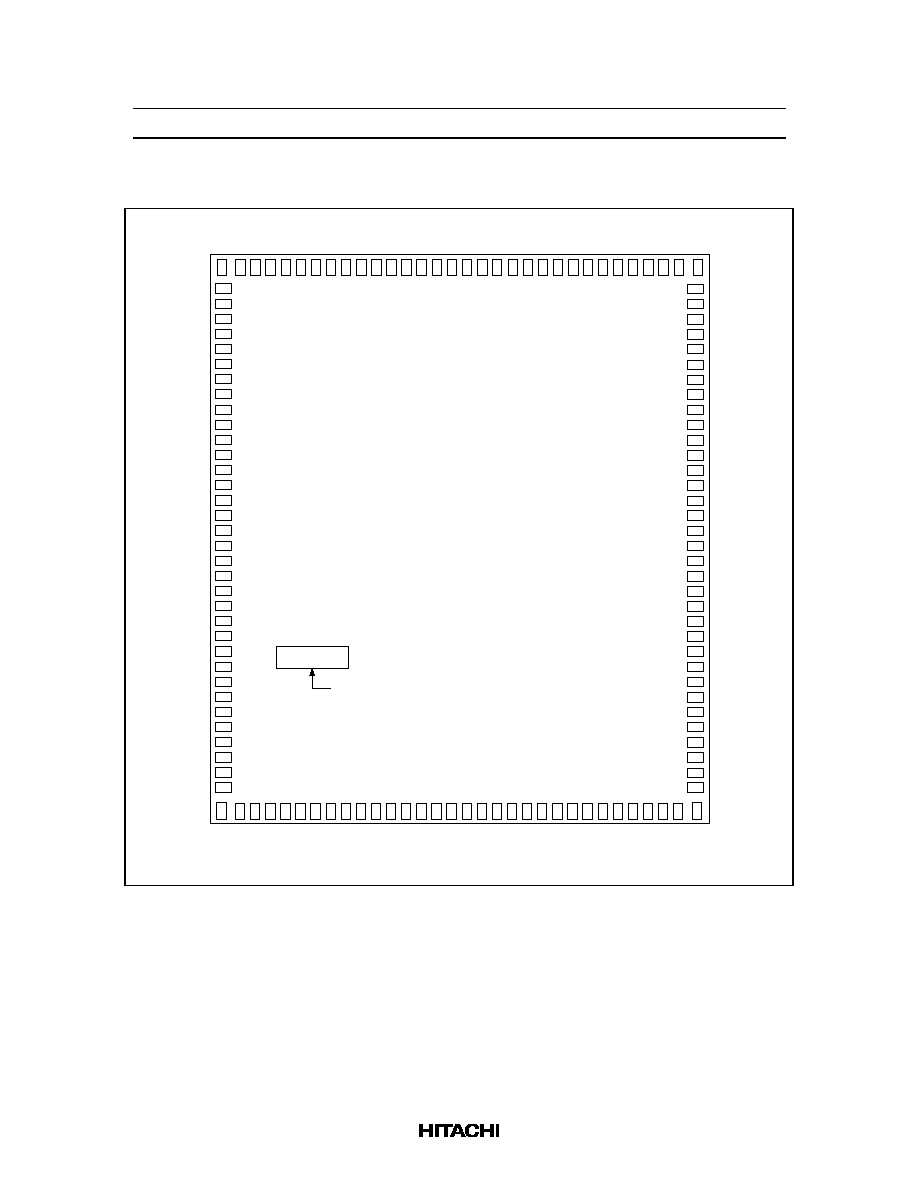
HD66712 Pin Arrangement
SEG17
SEG16
SEG15
SEG14
SEG13
SEG12
SEG11
SEG10
SEG9
SEG8
SEG7
SEG6
SEG5
SEG4
SEG3
SEG2
SEG1
COM0
COM1
COM2
COM3
COM4
COM5
COM6
COM7
COM8
COM17
COM18
COM19
COM20
COM21
COM22
COM23
COM24
V1
V2
V3
V4
SEG43
SEG42
SEG41
SEG40
SEG39
SEG38
SEG37
SEG36
SEG35
SEG34
SEG33
SEG32
SEG31
SEG30
SEG29
SEG28
SEG27
SEG26
SEG25
SEG24
SEG23
SEG22
SEG21
SEG20
SEG19
SEG18
CL2
D
M
RESET
*
IM
EXT
TEST
GND
RS/CS
*
RW/SID
E/SCLK
DB0/SOD
DB1
DB2
DB3
DB4
DB5
DB6
DB7
Vci
C2
C1
GND
V5OUT2
V5OUT3
V5
SEG44
SEG45
SEG46
SEG47
SEG48
SEG49
SEG50
SEG51
SEG52
SEG53
SEG54
SEG55
SEG56
SEG57
SEG58
SEG59
SEG60
COM9
COM10
COM11
COM12
COM13
COM14
COM15
COM16
COM25
COM26
COM27
COM28
COM29
COM30
COM31
COM32
COM33
V
CC
OSC2
OSC1
CL1
1
2
3
4
5
6
7
8
9
10
11
12
13
14
15
16
17
18
19
20
21
22
23
24
25
26
27
28
29
30
31
32
33
34
35
36
37
38
102
101
100
99
98
97
96
95
94
93
92
91
90
89
88
87
86
85
84
83
82
81
80
79
78
77
76
75
74
73
72
71
70
69
68
67
66
65
39
40
41
42
43
44
45
46
47
48
49
50
51
52
53
54
55
56
57
58
59
60
61
62
63
64
HD66712S
(Top view)
128
127
126
125
124
123
122
121
120
119
118
117
116
115
114
113
112
111
110
109
108
107
106
105
104
103
HD66712U
373
TCP Dimensions
0.24-mm pitch
COM33
COM32
COM25
COM16
COM9
SEG60
SEG1
COM0
COM1
COM8
COM17
COM24
LCD driver output side
I/O/power supply side
0.65-mm pitch
NC
V
CC
OSC2
OSC1
CL1
CL2
D
M
RESET
*
IM
EXT
TEST
GND
RS/CS
*
RW/SID
E/SCLK
DB0/SOD
DB1
DB2
DB3
DB4
DB5
DB6
DB7
Vci
C2
C1
GND
V5OUT2
V5OUT3
V5
V4
V3
V2
V1
NC
HD66712U
374
HCD66712U Pad Arrangement
HCD66712U
SEG46
SEG47
SEG48
SEG49
SEG50
SEG51
SEG52
SEG53
SEG54
SEG55
SEG56
SEG57
SEG58
SEG59
SEG60
COM9
COM10
COM11
COM12
COM13
COM14
COM15
COM16
COM25
COM26
COM27
COM28
COM29
COM30
COM31
COM32
COM33
V
CC
OSC2
3
4
5
6
7
8
9
10
11
12
13
14
15
16
17
18
19
20
21
22
23
24
25
26
27
28
29
30
31
32
33
34
35
36
SEG15
SEG14
SEG13
SEG12
SEG11
SEG10
SEG9
SEG8
SEG7
SEG6
SEG5
SEG4
SEG3
SEG2
SEG1
COM0
COM1
COM2
COM3
COM4
COM5
COM6
COM7
COM8
COM17
COM18
COM19
COM20
COM21
COM22
COM23
COM24
V1
V2
100
99
98
97
96
95
94
93
92
91
90
89
88
87
86
85
84
83
82
81
80
79
78
77
76
75
74
73
72
71
70
69
68
67
2
1
128
127
126
125
124
123
122
121
120
119
118
117
116
115
114
113
112
111
110
109
108
107
106
105
104
103
102
101
SEG45
SEG44
SEG43
SEG42
SEG41
SEG40
SEG39
SEG38
SEG37
SEG36
SEG35
SEG34
SEG33
SEG32
SEG31
SEG30
SEG29
SEG28
SEG27
SEG26
SEG25
SEG24
SEG23
SEG22
SEG21
SEG20
SEG19
SEG18
SEG17
SEG16
37
38
39
40
41
42
43
44
45
46
47
48
49
50
51
52
53
54
55
56
57
58
59
60
61
62
63
64
65
66
OSC1
CL1
CL2
D
M
RESET*
IM
EXT
TEST
GND
RS/CS*
RW/SID
E/SCLK
DB0/SOD
DB1
DB2
DB3
DB4
DB5
DB6
DB7
Vci
C2
C1
GND
V5OUT2
V5OUT3
V5
V4
V3
(Top view)
HD66712
Type code

HD66712U
375
Pin Functions
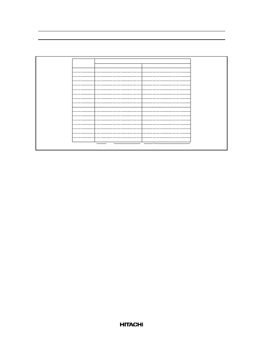
Table 1
Pin Functional Description
Signal
Number
of Pins
I/O
Device
Interfaced with
Function
IM
1
I
--
Selects interface mode with the MPU;
Low: Serial mode
High: 4-bit/8-bit bus mode
(Bus width is specified by instruction.)
RS/CS*
1
I
MPU
Selects registers during bus mode:
Low: Instruction register (write);
Busy flag, address counter (read)
High: Data register (write/read)
Acts as chip-select during serial mode:
Low: Select (access enable)
High: Not selected (access disable)
RW/SID
1
I
MPU
Selects read/write during bus mode;
Low: Write
High: Read
Inputs serial data during serial mode.
E/SCLK
1
I
MPU
Starts data read/write during bus mode;
Inputs (Receives) serial clock during serial mode.
DB4 to
DB7
4
I/O
MPU
Four high-order bidirectional tristate data bus pins.
Used for data transfer between the MPU and the
HD66712. DB7 can be used as a busy flag. Open
these pins during serial mode since those signals.
DB1 to
DB3
3
I/O
MPU
Three low order bidirectional tristate data bus pins.
Used for data transfer between the MPU and the
HD66712. Open these pins during 4-bit operation or
serial mode since they are not used.
DB0/ SOD
1
I/O
/O
MPU
The lowest bidirectional data bit (DB0) during 8-bit bus
mode. Open these pins during 4-bit mode since they
are not used.
Outputs (transfers) serial data during serial mode.
Open this pin if reading (transfer) is not performed.
COM0 to
COM33
34
O
LCD
Common signals; those that are not used become non-
selected waveforms. At 1/17 duty rate, COM1 to
COM16 are used for character display, COM0 and
COM17 for icon display, and COM18 to COM33
become non-selected waveforms. At 1/33 duty rate,
COM1 to COM32 are used for character display, and
COM0 and COM33 for icon display. Because two COM
signals output the same level simultaneously, apply
them according to the wiring pattern of the display
device.
SEG1 to
SEG60
60
O
LCD
Segment output signals

HD66712U
376
Table 1
Pin Functional Description (cont)
Signal
Number
of Pins
I/O
Device
Interfaced with
Function
CL1
1
O
Extension driver
When EXT = high, outputs the extension driver latch
pulse.
CL2
1
O
Extension driver
When EXT = high, outputs the extension driver shift
clock.
D
1
O
Extension driver
When EXT = high, outputs extension driver data; data
from the 61st dot on is output.
M
1
O
Extension driver
When EXT = high, outputs the extension driver AC
signal.
EXT
1
I
--
When EXT = high, outputs the extension driver
control signal. When EXT = low, the signal becomes
tristate and can suppress consumption current.
V1 to V5
5
--
Power supply
Power supply for LCD drive
V
CC
≠V5 = 11V (max)
V
CC
/GND
2
--
Power supply
V
CC
: +2.7V to +5.5V, GND: 0V
OSC1/
OSC2
2
--
Oscillation resistor
clock
When crystal oscillation is performed, an external
resistor must be connected. When the pin input is an
external clock, it must be input to OSC1.
Vci
1
I
--
Inputs voltage to the booster to generate the liquid
crystal display drive voltage.
Vci is reference voltage and power supply for the
booster.
Vci = 1.0V to 5.0V
V
CC
V5OUT2
1
O
V5 pin/ booster
capacitance
Voltage input to the Vci pin is boosted twice and
output. When the voltage is boosted three times, the
same capacitance as that of C1≠C2 should be
connected here.
V5OUT3
1
O
V5 pin
Voltage input to the Vci pin is boosted three times and
output.
C1/C2
2
--
Booster
capacitance
External capacitance should be connected here when
using the booster.
RESET*
1
I
--
Reset pin. Initialized to "low."
TEST
1
I
--
Test pin. Should be wired to ground.

HD66712U
377
Function Description
System Interface
The HD66712 has three types of system interfaces: synchronized serial, 4-bit bus, and 8-bit bus. The
serial interface is selected by the IM-pin, and the 4/8-bit bus interface is selected by the DL bit in the
instruction register.
The HD66712 has two 8-bit registers: an instruction register (IR) and a data register (DR).
The IR stores instruction codes, such as display clear and cursor shift, and address information for the
display data RAM (DDRAM), the character generator RAM (CGRAM), and the segment RAM
(SEGRAM). The MPU can only write to IR, and cannot be read from.
The DR temporarily stores data to be written into DDRAM, CGRAM, or SEGRAM. Data written into the
DR from the MPU is automatically written into DDRAM, CGRAM, or SEGRAM by an internal
operation. The DR is also used for data storage when reading data from DDRAM, CGRAM, or
SEGRAM. When address information is written into the IR, data is read and then stored into the DR from
DDRAM or CGRAM by an internal operation. Data transfer between the MPU is then completed when
the MPU reads the DR. After the read, data in DDRAM, CGRAM, or SEGRAM at the next address is
sent to the DR for the next read from the MPU.
These two registers can be selected by the registor selector (RS) signal in the 4/8 bit bus interface, and by
the RS bit in start byte data in synchronized serial interface (Table 2).
Busy Flag (BF)
When the busy flag is 1, the HD66712 is in the internal operation mode, and the next instruction will not
be accepted. When RS = 0 and R/W = 1 (Table 2), the busy flag is output from DB7. The next instruction
must be written after ensuring that the busy flag is 0.
Address Counter (AC)
The address counter (AC) assigns addresses to DDRAM, CGRAM, or SEGRAM. When an address of an
instruction is written into the IR, the address information is sent from the IR to the AC. Selection of
DDRAM, CGRAM, and SEGRAM is also determined concurrently by the instruction.
After writing into (reading from) DDRAM, CGRAM, or SEGRAM, the AC is automatically incremented
by 1 (decremented by 1). The AC contents are then output to DB0 to DB6 when RS = 0 and R/
: = 1
(Table 2).
HD66712U
378
Table 2
Resistor Selection
RS
R/
:
:
Operation
0
0
IR write as an internal operation (display clear, etc.)
0
1
Read busy flag (DB7) and address counter (DB0 to DB6)
1
0
DR write as an internal operation (DR to DDRAM, CGRAM, or SEGRAM)
1
1
DR read as an internal operation (DDRAM, CGRAM, or SEGRAM to DR)
Display Data RAM (DDRAM)
Display data RAM (DDRAM) stores display data represented in 8-bit character codes. Its capacity is 80
◊
8 bits, or 80 characters. The area in display data RAM (DDRAM) that is not used for display can be used
as general data RAM.
The DDRAM address (A
DD
) is set in the address counter (AC) as a hexadecimal number, as shown in
Figure 1.
The relationship between DDRAM addresses and positions on the liquid crystal display is described and
shown on the following pages for a variety of cases.
AC6 AC5 AC4 AC3 AC2 AC1 AC0
AC
MSB
LSB
1
0
0
1
1
1
0
Example: DDRAM address 4E
Figure 1 DDRAM Address
HD66712U
379
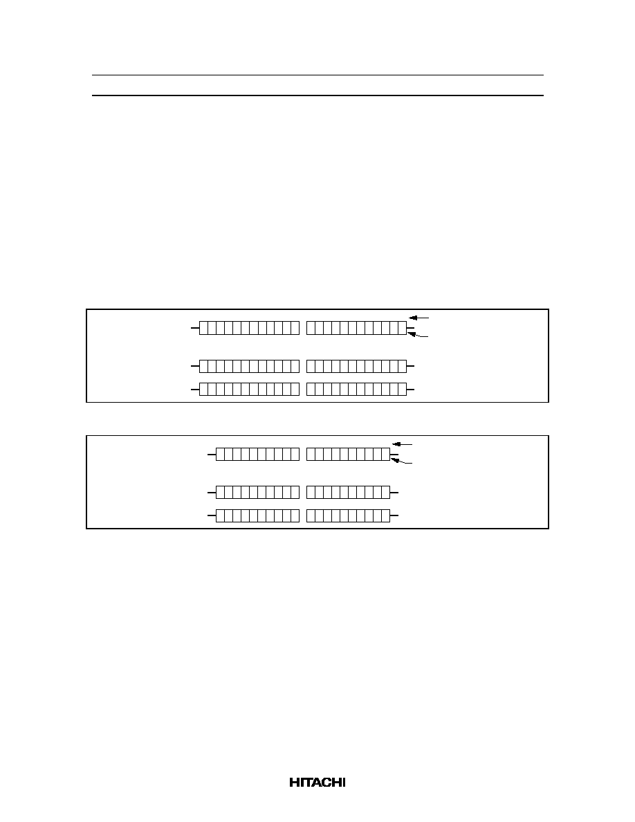
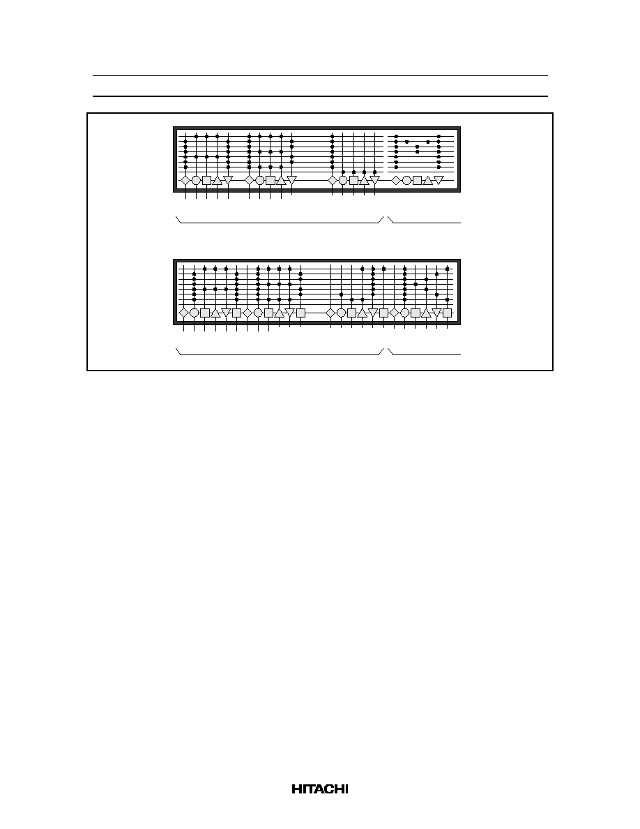
∑
1-line display (N = 0, and NW = 0)
Case 1: When there are fewer than 80 display characters, the display begins at the beginning of
DDRAM. For example, when 24 5-dot font-width characters are displayed using one HD66712,
the display is generated as shown in Figure 2.
When a display shift is performed, the DDRAM addresses shift as well as shown in the figure.
When 20 6-dot font-width characters are displayed using one HD66712, the display is generated as
shown in Figure 3. Note that COM9 to COM16 begins at address (0A)H in this case 20 characters
are displayed.
When a display shift is performed, the DDRAM addresses shift as well as shown in the figure.
Case 2: Figure 4 shows the case where the EXT pin is fixed high and the HD66712 and the 40-
output extension driver are used to display 24 6-dot font-width characters. In this case, COM9 to
COM16 begins at (0A)H.
When a display shift is performed, the DDRAM addresses shift as well as shown in the figure.
COM1 to 8
COM9 to 16
COM1 to 8
COM9 to 16
(Left shift display)
COM1 to 8
COM9 to 16
(Right shift display)
Display position
DDRAM address
00 01 02 03 04
06
05
1 2 3 4 5 6 7 8
07
COM1 to 8
0C 0D 0E 0F 10
12
11
13 14 15 16 17 18 19 20
13
01 02 03 04 05
07
06
1 2 3 4 5 6 7 8
08
0D 0E 0F 10 11
13
12
13 14 15 16 17 18 19 20
14
4F 00 01 02 03
05
04
06
0B 0C 0D 0E 0F
11
10
12
9
08
9
09
07
10
09
10
0A
08
11
0A
11
0B
09
0B
0C
0A
12
12
21
14
21
15
13
22
15
22
16
14
23
16
23
17
15
24
17
24
18
16
Figure 2 1-Line by 24-Character Display (5-Dot Font Width)
COM1 to 8
COM9 to 16
COM1 to 8
COM9 to 16
(Left shift display)
COM1 to 8
COM9 to 16
(Right shift display)
Display position
DDRAM address
00 01 02 03 04
06
05
1 2 3 4 5 6 7 8
07
COM1 to 8
0A 0B 0C 0D 0E
10
0F
11 12 13 14 15 16 17 18
11
01 02 03 04 05
07
06
1 2 3 4 5 6 7 8
08
0B 0C 0D 0E 0F
11
10
11 12 13 14 15 16 17 18
12
4F 00 01 02 03
05
04
06
09 0A 0B 0C 0D
0F
0E
10
9
08
9
09
07
10
09
10
0A
08
19
12
19
13
11
20
20
14
12
13
Figure 3 1-Line by 20-Character Display (6-Dot Font Width)
HD66712U
380
01 02 03 04
06
05
07
0B 0C 0D 0E 0F
15 16
COM1 to 8
COM9 to 16
(Left shift display)
1 2 3 4 5 6 7
11 12 13 14 15
21 22 23
00 01 02 03 04 05
09 0A 0B 0C 0D
13 14 15
COM1 to 8
COM9 to 16
(Right shift display)
4F
17
00 01 02 03 04
06
05
0A 0B 0C 0D 0E
14 15 16
COM1 to 8
COM9 to 16
1 2 3 4 5 6 7
11 12 13 14 15
21 22 23
HD66712
SEG1 to SEG60
HD66712
SEG1 to SEG60
Extension driver
SEG1 to SEG24
Display position
DDRAM address
08
8
06
07
8
09
9
07
08
9
0A
10
08
09
10
10
16
0E
0F
16
11
17
0F
10
17
12
18
10
11
18
13
19
11
12
19
14
20
12
13
20
24
18
17
24
16
Figure 4 1-Line by 24-Character Display (6-Dot Font Width)

HD66712U
381
∑
2-line display (N = 1, and NW = 0)
Case 1: The first line is displayed from COM1 to COM16, and the second line is displayed from
COM17 to COM32. Note that the last address of the first line and the first address of the second
line are not consecutive. Figure 5 shows an example where a 5-dot font-width 24
◊
2-line display
is performed using one HD66712. Here, COM9 to COM16 begins at (0C)H, and COM25 to
COM32 at (4C)H. When a display shift is performed, the DDRAM addresses shift as shown.
Figure 6 shows an example where a 6-dot font-width 20
◊
2-line display is performed using one
HD66712. COM9 to COM16 begins at (0A)H, and COM25 to COM32 at (4A)H.
COM1 to
COM8
COM9 to COM16
Display position
00 01 02 03 04
06
05
1 2 3 4 5 6 7 8
07
0C 0D 0E 0F 10
12
11
13 14 15 16 17 18 19 20
13
9
08
10
09
11
0A 0B
12
21
14
22
15
23
16
24
17
COM1 to
COM8
COM9 to
COM16
COM1 to
COM8
COM9 to
COM16
COM1
01 02 03 04 05
07
06
1 2 3 4 5 6 7 8
08
0D 0E 0F 10 11
13
12
13 14 15 16 17 18 19 20
14
27 00 01 02 03
05
04
06
0B 0C 0D 0E 0F
11
10
12
9
09
07
10
0A
08
11
0B
09
0C
0A
12
21
15
13
22
16
14
23
17
15
24
18
16
COM17 to
COM24
COM25 to COM32
DDRAM address
40 41 42 43 44
46
45
47
4C 4D 4E 4F 50
52
51
53
48 49 4A 4B
54 55 56 57
COM17 to
COM24
COM25 to
COM32
COM1
41 42 43 44 45
47
46
48
4D 4E 4F 50 51
53
52
54
49 4A 4B 4C
55 56 57 58
COM17 to
COM24
COM25 to
COM32
67 40 41 42 43
45
44
46
4B 4C 4D 4E 4F
51
50
52
47 48 49 4A
53 54 55 56
(Left shift
display)
(Right shift
display)
Figure 5 2-Line by 24-Character Display (5-Dot Font Width)
COM1 to
COM8
COM9 to COM16
Display position
00 01 02 03 04
06
05
1 2 3 4 5 6 7 8
07
0A 0B 0C 0D 0E
11
10
11 12 13 14 15 16 17 18
12
9
08
10
09
19
13
20
COM17 to
COM24
COM25 to COM32
DDRAM address
40 41 42 43 44
46
45
47
4A 4B 4C 4D 4E
50
4F
51
48 49
52 53
0F
Figure 6 2-Line by 20-Character Display (6-Dot Font Width)

HD66712U
382
Case 2: Figure 7 shows the case where the EXT pin is fixed high and the HD66712 and the 40-
output extension driver are used to extend the number of display characters to 32 5-dot font-width
characters.
In this case, COM9 to COM16 begins at (0C)H, and COM25 to COM32 at (4C)H.
When a display shift is performed, the DDRAM addresses shift as shown.
COM1 to
COM8
00 01 02 03 04
06
05
1 2 3 4 5 6 7 8
07
0C 0D 0E 0F 10
12
11
13 14 15 16 17 18 19 20
13
9
08
10
09
11
0A 0B
12
21
14
22
15
23
16
24
17
COM1 to
COM8
COM1 to
COM8
COM1
01 02 03 04 05
07
06
1 2 3 4 5 6 7 8
08
0D 0E 0F 10 11
13
12
13 14 15 16 17 18 19 20
14
27 00 01 02 03
05
04
06
0B 0C 0D 0E 0F
11
10
12
9
09
07
10
0A
08
11
0B
09
0C
0A
12
21
15
13
22
16
14
23
17
15
24
18
16
COM17 to
COM24
40 41 42 43 44
46
45
47
4C 4D 4E 4F 50
52
51
53
48 49 4A 4B
54 55 56 57
COM17 to
COM24
COM1
41 42 43 44 45
47
46
48
4D 4E 4F 50 51
53
52
54
49 4A 4B 4C
55 56 57 58
COM17 to
COM24
67 40 41 42 43
45
44
46
4B 4C 4D 4E 4F
51
50
52
47 48 49 4A
53 54 55 56
COM9 to COM16
Display position
18 19 1A 1B 1C
1E
1D
25 26 27 28 29 30 31 32
1F
COM9 to COM16
COM9 to COM16
25 26 27 28 29 30 31 32
17 18 19 1A 1B
1D
1C
1E
COM25 to COM32
DDRAM address
58 59 5A 5B 5C
5E
5D
5F
COM25 to COM32
59 5A 5B 5C 5D
5F
5E
60
COM25 to COM32
57 58 59 5A 5B
5D
5C
5E
(Left shift display)
(Right shift display)
19 1A 1B 1C 1D
1F
1E
20
HD66712
SEG1≠SEG60
HD66712
SEG1≠SEG60
Extension driver
Seg1≠Seg40
Figure 7 2-Line by 32 Character Display (5-Dot Font Width)

HD66712U
383
∑
4-line display (NW = 1)
Case 1: The first line is displayed from COM1 to COM8, the second line is displayed from COM9
to COM16, the third line is displayed from COM17 to COM24, and the fourth line is displayed
from COM25 to COM32.
Note that the DDRAM addresses of each line are not consecutive. Figure 8 shows an example
where a 12
◊
4-line display is performed using one HD66712.
When a display shift is performed, the DDRAM addresses shift as shown.
(Left shift display)
01 02 03 04 05 06
21 22 23 24 25 26
COM1 to 8
COM17 to 24
COM9 to 16
COM25 to 32
1 2 3 4 5 6 7
41 42 43 44 45 46
61 62 63 64 65 66
07
27
67
8
28
48
47
08
68
(Right shift display)
1 2 3 4 5 6 7
13
33
53
00 01 02 03 04 05 06
20 21 22 23 24 25 26
40 41 42 43 44 45 46
60 61 62 63 64 65 66
73
8
00 01 02 03 04 05 06
20 21 22 23 24 25 26
COM1 to 8
COM17 to 24
COM9 to 16
COM25 to 32
1 2 3 4 5 6 7
40 41 42 43 44 45 46
60 61 62 63 64 65 66
Display position
DDRAM address
07
27
8
47
67
08
28
9
48
68
09
29
10
49
69
0A
2A
11
4A
6A
0B
2B
12
4B
6B
9
29
49
09
69
10
2A
4A
0A
6A
11
2B
4B
0B
6B
12
2C
4C
0C
6C
07
27
47
67
9
08
28
48
68
10
09
29
49
69
11
0A
2A
4A
6A
12
Figure 8 4-Line Display

HD66712U
384
Case 2: Figure 9 shows the case where the EXT pin is fixed high and the HD66712 and the 40-
output extension driver are used to extend the number of display characters.
When a display shift is performed, the DDRAM addresses shift as shown.
1 2 3 4 5 6 7 8 9 10 11 12 13 14 15 16 17 18 19 20
4E
1 2 3 4 5 6 7 8 9 10 11 12 13 14 15 16 17 18 19 20
01 02 03 04 05 06
11 12 13
0A 0B 0C
0D 0E 0F 10
07 08 09
00
21 22 23 24 25 26
31 32 33
2A 2B 2C
2D 2E 2F 30
27 28 29
20
41 42 43 44 45 46
51 52 53
4A 4B 4C
4D
4F 50
47 48 49
40
61 62 63 64 65 66
71 72 73
6A 6B 6C
6D 6E 6F 70
67 68 69
60
00 01 02 03 04 05 06
11 12
0A
0B 0C 0D 0E 0F 10
07 08 09
13
20 21 22 23 24 25 26
31 32
2A
2B 2C 2D 2E 2F 30
27 28 29
33
40 41 42 43 44 45 46
51 52
4A
4B 4C 4D 4E 4F 50
47 48 49
53
60 61 62 63 64 65 66
71 72
6A
6B 6C 6D 6E 6F 70
67 68 69
73
(Right shift display)
(Left shift display)
00 01 02 03 04 05 06
20 21 22 23 24 25 26
COM1 to 8
COM17 to 24
COM9 to 16
COM25 to 32
1 2 3 4 5 6 7 8 9 10 11 12 13 14 15 16 17 18 19 20
40 41 42 43 44 45 46
60 61 62 63 64 65 66
11 12 13
0A 0B
0C 0D 0E 0F 10
07 08 09
31 32 33
2A 2B
2C 2D 2E 2F 30
27 28 29
51 52 53
4A 4B
4C 4D 4E 4F 50
47 48 49
71 72 73
6A 6B
6C 6D 6E 6F 70
67 68 69
HD66712
Extension driver
Display position
DDRAM address
Figure 9 4-Line by 20-Character Display

HD66712U
385
Character Generator ROM (CGROM)
The character generator ROM generates 5
◊
8 dot character patterns from 8-bit character codes (Table 3
to 6). It can generate 240 5
◊
8 dot character patterns. User-defined character patterns are also available
using a mask-programmed ROM (see "Modifying Character Patterns.")
Character Generator RAM (CGRAM)
The character generator RAM allows the user to redefine the character patterns. In the case of 5
◊
8
characters, up to eight may be redefined.
Write the character codes at the addresses shown as the left column of Table 3 to 6 to show the character
patterns stored in CGRAM.
See Table 7 for the relationship between CGRAM addresses and data and display patterns.
Segment RAM (SEGRAM)
The segment RAM (SEGRAM) is used to enable control of segments such as an icon and a mark by the
user program.
For a 1-line display, SEGRAM is read from the COM0 and the COM17 output, and for 2- or 4-line
displays, it is read from the COM0 and the COM33 output, to perform 60-segment display (80-segment
display when using the extension driver).
As shown in Table 8, bits in SEGRAM corresponding to segments to be displayed are directly set by the
MPU, regardless of the contents of DDRAM and CGRAM.
SEGRAM data is stored in eight bits. The lower six bits control the display of each segment, and the
upper two bits control segment blinking.
Timing Generation Circuit
The timing generation circuit generates timing signals for the operation of internal circuits such as
DDRAM, CGROM, CGRAM, and SEGRAM. RAM read timing for display and internal operation timing
by MPU access are generated separately to avoid interfering with each other. Therefore, when writing
data to DDRAM, for example, there will be no undesirable interferences, such as flickering, in areas
other than the display area.

HD66712U
386
Liquid Crystal Display Driver Circuit
The liquid crystal display driver circuit consists of 34 common signal drivers and 60 segment signal
drivers. When the character font and number of lines are selected by a program, the required common
signal drivers automatically output drive waveforms, while the other common signal drivers continue to
output non-selection waveforms.
Character pattern data is sent serially through a 60-bit shift register and latched when all needed data has
arrived. The latched data then enables the driver to generate drive waveform outputs.
Sending serial data always starts at the display data character pattern corresponding to the last address of
the display data RAM (DDRAM).
Since serial data is latched when the display data character pattern corresponding to the starting address
enters the internal shift register, the HD66712 drives from the head display.
Cursor/Blink Control Circuit
The cursor/blink (or white-black inversion) control is used to produce a cursor or a flashing area on the
display at a position corresponding to the location in stored in the address counter (AC).
For example (Figure 10), when the address counter is (08)H, a cursor is displayed at a position
corresponding to DDRAM address (08)H.
Scroll Control Circuit
The scroll control circuit is used to perform a smooth-scroll in the unit of dot. When the number of
characters to be displayed is greater than that possible at one time on the liquid crystal module, this
horizontal smooth scroll can be used to display all characters.
AC = (08)16
00
1
Cursor position
Display position
DDRAM address
01
2
02
3
03
4
04
5
05
6
06
7
07
8
08
9
09
10
0A
11
Figure 10 Cursor/Blink Display Example
HD66712U
387
Table 3
Relationship between Character Codes and Character Patterns (ROM Code: A00)
xxxx0000
xxxx0001
xxxx0010
xxxx0011
xxxx0100
xxxx0101
xxxx0110
xxxx0111
xxxx1000
xxxx1001
xxxx1010
xxxx1011
xxxx1100
xxxx1101
xxxx1110
xxxx1111
0000
0010 0011 0100 0101 0110 0111
1010 1011 1100 1101 1110 1111
Upper
Bits
Lower
Bits
CG
RAM
(1)
0001
1000 1001
CG
RAM
(2)
CG
RAM
(3)
CG
RAM
(4)
CG
RAM
(5)
CG
RAM
(6)
CG
RAM
(7)
CG
RAM
(8)
CG
RAM
(1)
CG
RAM
(2)
CG
RAM
(3)
CG
RAM
(4)
CG
RAM
(5)
CG
RAM
(6)
CG
RAM
(7)
CG
RAM
(8)

HD66712U
388
Table 4
Relationship between Character Codes and Character Pattern (ROM Code: A01)
xxxx0000
xxxx0001
xxxx0010
xxxx0011
xxxx0100
xxxx0101
xxxx0110
xxxx0111
xxxx1000
xxxx1001
xxxx1010
xxxx1011
xxxx1100
xxxx1101
xxxx1110
xxxx1111
0000
0010 0011 0100 0101 0110 0111
1010 1011 1100 1101 1110 1111
Upper
Bits
Lower
Bits
CG
RAM
(1)
0001
1000 1001
CG
RAM
(2)
CG
RAM
(3)
CG
RAM
(4)
CG
RAM
(5)
CG
RAM
(6)
CG
RAM
(7)
CG
RAM
(8)
CG
RAM
(1)
CG
RAM
(2)
CG
RAM
(3)
CG
RAM
(4)
CG
RAM
(5)
CG
RAM
(6)
CG
RAM
(7)
CG
RAM
(8)
HD66712U
389
Table 5
Relationship between Character Codes and Character Patterns (ROM Code: A02)
xxxx0000
xxxx0001
xxxx0010
xxxx0011
xxxx0100
xxxx0101
xxxx0110
xxxx0111
xxxx1000
xxxx1001
xxxx1010
xxxx1011
xxxx1100
xxxx1101
xxxx1110
xxxx1111
0000
0010 0011 0100 0101 0110 0111
1010 1011 1100 1101 1110 1111
Upper
Bits
Lower
Bits
CG
RAM
(1)
0001
1000 1001
CG
RAM
(2)
CG
RAM
(3)
CG
RAM
(4)
CG
RAM
(5)
CG
RAM
(6)
CG
RAM
(7)
CG
RAM
(8)
CG
RAM
(1)
CG
RAM
(2)
CG
RAM
(3)
CG
RAM
(4)
CG
RAM
(5)
CG
RAM
(6)
CG
RAM
(7)
CG
RAM
(8)
Note: The character codes of the characters enclosed in the bold frame are the same as those of the first
edition of the ISO8859 and the character code compatible.
HD66712U
390
Table 6
Relationship between Character Codes and Character Pattern (ROM Code: A03)
xxxx0000
xxxx0001
xxxx0010
xxxx0011
xxxx0100
xxxx0101
xxxx0110
xxxx0111
xxxx1000
xxxx1001
xxxx1010
xxxx1011
xxxx1100
xxxx1101
xxxx1110
xxxx1111
0000
0010 0011 0100 0101 0110 0111
1010 1011 1100 1101 1110 1111
Upper
Bits
Lower
Bits
CG
RAM
(1)
0001
1000 1001
CG
RAM
(2)
CG
RAM
(3)
CG
RAM
(4)
CG
RAM
(5)
CG
RAM
(6)
CG
RAM
(7)
CG
RAM
(8)
CG
RAM
(1)
CG
RAM
(2)
CG
RAM
(3)
CG
RAM
(4)
CG
RAM
(5)
CG
RAM
(6)
CG
RAM
(7)
CG
RAM
(8)
HD66712U
391
Table
7
Example of Relationships between Character Code (DDRAM) and Character
Pattern(CGRAM Data)
D7 D6 D5 D4 D3 D2 D1 D0
Character code (DDRAM data)
CGRAM data
LSB
MSB
A2 A1 A0
A5 A4 A3
0
0
0
0
0
0
1
0
1
0
0
1
1
1
0
0
1
0
1
1
1
0
1
1
1
0
0
*
0
0
0
0
1
0
0
0
1
1
0
0
0
1
1
0
0
0
1
0
1
0
1
0
0
0
1
0
0
0
0
1
0
0
0
0
1
0
0
0
0
0
0
0
0
0
0
*
*
*
O4 O3 O2 O1 O0
O5
O6
O7
CGRAM address
1
1
1
0
0
0
0
0
*
*
1
0
0
0
0
0
1
0
1
0
0
1
1
1
0
0
1
0
1
1
1
0
1
1
*
0
0
0
0
1
0
0
0
1
1
0
0
0
1
1
0
0
0
1
0
1
0
1
0
0
0
1
0
0
0
0
1
0
0
0
0
1
0
0
1
1
1
*
Character
pattern
(1)
Character
pattern
(8)
D7 D6 D5 D4 D3 D2 D1 D0
LSB
MSB
A2 A1 A0
A5 A4 A3
O4 O3 O2 O1 O0
O5
O6
O7
0
0
0
0
0
0
1
0
1
0
0
1
1
1
0
0
1
0
1
1
1
0
1
1
1
0
0
*
0
0
0
0
1
0
0
0
1
1
0
0
0
1
1
0
0
0
1
0
1
0
1
0
0
0
1
0
0
0
0
1
0
0
0
0
1
0
0
0
0
0
0
0
0
0
0
*
*
0
0
0
0
0
0
0
0
0
1
1
1
0
0
0
0
1
0
0
0
0
0
1
0
1
0
0
1
1
1
0
0
1
0
1
1
1
0
1
1
*
0
0
0
0
1
0
0
0
1
1
0
0
0
1
1
0
0
0
1
0
1
0
1
0
0
0
1
0
0
0
0
1
0
0
0
0
1
0
0
1
1
1
*
0
0
0
0
0
0
0
0
Character
pattern
(1)
Character
pattern
(8)
Character code (DDRAM data)
CGRAM address
CGRAM data
*
a) When character pattern is 5
◊
8 dots
a) When character pattern is 6
◊
8 dots

HD66712U
392
Notes: 1. Character code bits 0 to 2 correspond to CGRAM address bits 3 to 5 (3 bits: 8 types).
2. CGRAM address bits 0 to 2 designate the character pattern line position. The 8th line is the
cursor position and its display is formed by a logical OR with the cursor.
3. The character data is stored with the rightmost character element in bit 0, as shown in the
figure above. Characters of 5 dots in width (FW = 0) are stored in bits 0 to 4, and characters of
6 dots in width (FW = 1) are stored in bits 0 to 5.
4. When the upper four bits (bits 7 to 4) of the character code are 0, CGRAM is selected.
Bit 3 of the character code is invalid (*). Therefore, for example, the character codes (00)H and
(08)H correspond to the same CGRAM address.
5. A set bit in the CGRAM data corresponds to display selection, and 0 to non-selection.
6. When the BE bit of the function set register is 1, pattern blinking control of the lower six bits is
controlled using the upper two bits (bits 7 and 6) in CGRAM.
When bit 7 is 1, of the lower six bits, only those which are set are blinked on the display.
When bit 6 is 1, a bit 4 pattern can be blinked as for a 5-dot font width, and a bit 5 pattern
can be blinked as for a 6-dot font width.
*
Indicates no effect.
HD66712U
393
Table 8
Relationship between SEGRAM Addresses and Display Patterns
B1 B0
*
S1 S2 S3 S4 S5
B1 B0
S1 S2 S3 S4 S5 S6
*
S6 S7 S8 S9 S10
B1 B0
*
S11 S12 S13 S14 S15
B1 B0
*
S16 S17 S18 S19 S20
B1 B0
*
S21 S22 S23 S24 S25
B1 B0
*
S26 S27 S28 S29 S30
B1 B0
*
S31 S32 S33 S34 S35
B1 B0
*
*
*
*
*
*
*
*
*
S36
S41
S46
S51
S56
S61
S66
S71
S76
S37
S42
S47
S52
S57
S62
S67
S72
S77
S38
S43
S48
S53
S58
S63
S68
S73
S78
S39
S44
S49
S54
S59
S64
S69
S74
S79
S40
S45
S50
S55
S60
S65
S70
S75
S80
B1
B1
B1
B1
B1
B1
B1
B1
B1
B0
B0
B0
B0
B0
B0
B0
B0
B0
Blinking control
Pattern on/off
S7 S8 S9 S10 S11 S12
B1 B0
S13 S14 S15 S16 S17 S18
B1 B0
S19 S20 S21 S22 S23 S24
B1 B0
S25 S26 S27 S28 S29 S30
B1 B0
S31 S32 S33 S34 S35 S36
B1 B0
S37 S38 S39 S40 S41 S42
B1 B0
S43
S49
S55
S61
S67
S73
S79
S85
S91
S44
S50
S56
S62
S68
S74
S80
S86
S92
S45
S51
S57
S63
S69
S75
S81
S87
S93
S46
S52
S58
S64
S70
S76
S82
S88
S94
S47
S53
S59
S65
S71
S77
S83
S89
S95
S48
S54
S60
S66
S72
S78
S84
S90
S96
B1
B1
B1
B1
B1
B1
B1
B1
B1
B0
B0
B0
B0
B0
B0
B0
B0
B0
A0
0
1
0
1
0
1
0
1
0
1
0
1
0
1
0
1
A1
0
0
1
1
0
0
1
1
0
0
1
1
0
0
1
1
A2
0
0
0
0
1
1
1
1
0
0
0
0
1
1
1
1
D7 D6 D5 D4 D3 D2 D1 D0
D7 D6 D5 D4 D3 D2 D1 D0
SEGRAM
address
SEGRAM data
Blinking control
Pattern on/off
a) 5-dot font width
b) 6-dot font width
A3
0
0
0
0
0
0
0
0
1
1
1
1
1
1
1
1
Notes: 1. Data set to SEGRAM is output when COM0 and COM17 are selected, as for a 1-line display,
and output when COM0 and COM33 are selected, as for a 2-line or a 4-line display. COM0
and COM17 for a 1-line display and COM0 and COM33 for a 2-line or a 4-line display are the
same signals.
2. S1 to S96 are pin numbers of the segment output driver. S1 is positioned to the left of the
display. When the HD66712 is used by one chip, segments from S1 to S60 are displayed. An
extension driver displays the segments after S61.
3. After S80 output at 5-dot font and S96 output at 6-dot font, S1 output is repeated again.
4. As for a 5-dot font width, lower five bits (D4 to D0) are display on.off information of each
segment. For a 6-dot character width, the lower six bits (D5 to D0) are the display information
for each segment.
5. When the BE bit of the function set register is 1, pattern blinking of the lower six bits is
controlled using the upper two bits (bits 7 and 6) in SEGRAM.
When bit 7 is 1, only a bit set to "1" of the lower six bits is blinked on the display.
When bit 6 is 1, only a bit 4 pattern can be blinked as for a 5-dot font width, and only a bit 5
pattern can be blinked as for 6-dot font width.
6. Bit 5 (D5) is invalid for a 5-dot font width.
7. Set bits in the SEGRAM data correspond to display selection, and zeros to non-selection.
HD66712U
394
SEG56
SEG57
SEG58
SEG59
SEG60
SEG61
SEG62
SEG63
SEG64
SEG65
SEG1
SEG2
SEG3
SEG4
SEG5
SEG6
SEG7
SEG8
SEG9
SEG10
SEG56
SEG57
SEG58
SEG59
SEG60
SEG11
SEG12
SEG55
Seg61
Seg62
Seg63
Seg64
Seg65
Seg66
Displayed by HD66712
i) 5-dot font width (FW = 0)
ii) 6-dot font width (FW = 1)
S1
S2
S3
S4
S5
S6
S7
S8
S9
S10
S56
S57
S58
S59
S60
S61
S62
S63
S64
S65
S1
S2
S3
S4
S7
S8
S9
S10
S11
S55
S56
S57
S58
S59
S6
S12
S61
S62
S63
S64
S60
S65
S66
S5
SEG1
SEG2
SEG3
SEG4
SEG5
SEG6
SEG7
SEG8
SEG9
SEG10
Displayed by extension driver
Displayed by HD66712
Displayed by extension driver
Figure 11 Correspondence between SEGRAM and Segment Display

HD66712U
395
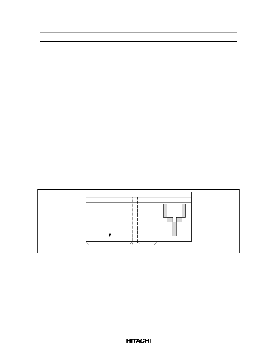
Modifying Character Patterns
∑
Character pattern development procedure
The following operations correspond to the numbers listed in Figure 12:
a. Determine the correspondence between character codes and character patterns.
b. Create a listing indicating the correspondence between EPROM addresses and data.
c. Program the character patterns into an EPROM.
d. Send the EPROM to Hitachi.
e. Computer processing of the EPROM is performed at Hitachi to create a character pattern listing,
which is sent to the user.
f. If there are no problems within the character pattern listing, a trial LSI is created at Hitachi and
samples are sent to the user for evaluation. When it is confirmed by the user that the character
patterns are correctly written, mass production of the LSI will proceed at Hitachi.
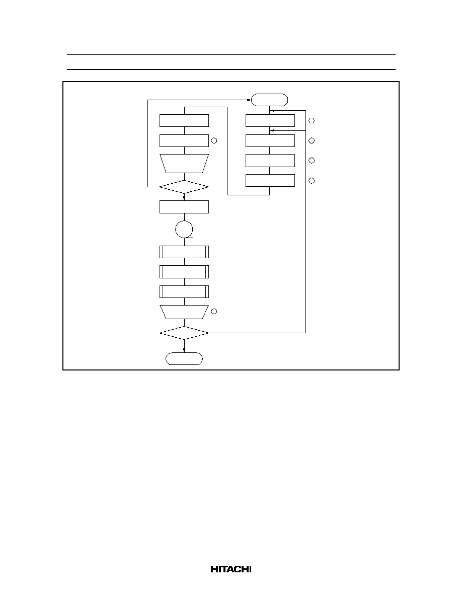
HD66712U
396
Determine
character patterns
Create EPROM
address data listing
Write EPROM
EPROM
Hitachi
Computer
processing
Create character
pattern listing
Evaluate
character
patterns
OK?
Art work
Sample
evaluation
OK?
Masking
Trial
Sample
No
Yes
No
Yes
M/T
1
3
2
4
5
6
User
Hitachi
Mass
production
Start
Figure 12 Character Pattern Development Procedure
HD66712U
397
Programming Character Patterns
This section explains the correspondence between addresses and data used to program character patterns
in EPROM.
∑
Programming to EPROM
The HD66712 character generator ROM can generate 240 5
◊
8 dot character patterns. Table 9 shows
correspondence between the EPROM address data and the character pattern.
Handling Unused Character Patterns
1. EPROM data outside the character pattern area: This is ignored by the character generator ROM for
display operation so any data is acceptable.
2. EPROM data in CGRAM area: Always fill with zeros.
3. Treatment of unused user patterns in the HD66712 EPROM: According to the user application, these
are handled in either of two ways:
a
When unused character patterns are not programmed: If an unused character code is written into
DDRAM, all its dots are lit, because the EPROM is filled with 1s after it is erased.
b
When unused character patterns are programmed as 0s: Nothing is displayed even if unused
character codes are written into DDRAM. (This is equivalent to a space.)
Table 9
Example of Correspondence between EPROM Address Data and Character Pattern
(5
◊
◊
8 Dots)
A10 A9 A8 A7 A6 A5 A4 A3
A2 A1 A0
0
0
0
0
0
1
0
1
0
0
1
1
1
0
0
1
0
1
1
1
0
1
1
1
1
0
0
0
1
O4 O3 O2 O1 O0
1
0
0
0
1
1
0
0
0
1
0
1
0
1
0
0
0
1
0
0
0
0
1
0
0
0
0
1
0
0
0
0
0
0
0
Character code
Line position
EPROM Address
Data
LSB
MSB
0
0
0
0
0
0
0
0
"0"
A11
0
1
0
1
1
0
0
1
Notes: 1. EPROM addresses A11 to A4 correspond to a character code.
2. EPROM addresses A2 to A0 specify the line position of the character pattern. EPROM address
A3 should be set to "0."
3. EPROM data O4 to O0 correspond to character pattern data.
4. Areas which are lit (indicated by shading) are stored as "1," and unlit areas as "0."
5. The eighth line is also stored in the CGROM, and should also be programmed. If the eighth line
is used for a cursor, this data should all be set to zero.
6. EPROM data bits 07 to 05 are invalid. 0 should be written in all bits.

HD66712U
398
Reset Function
Initializing by Internal Reset Circuit
An internal reset circuit automatically initializes the HD66712 when the power is turned on. The
following instructions are executed during the initialization. The busy flag (BF) is kept in the busy state
until the initialization ends (BF = 1). The busy state lasts for 15 ms after V
CC
rises to 4.5V or 40 ms after
the V
CC
rises to 2.7V.
1. Display clear:
(20)H to all DDRAM
2. Set functions:
DL = 1: 8-bit interface data
N = 1: 2-line display
RE = 0: Extension register write disable
BE = 0: CGRAM/SEGRAM blink off
LP = 0: Not in low power mode
3. Control display on/off:
D = 0: Display off
C = 0: Cursor off
B = 0: Blinking off
4. Set entry mode:
I/D = 1: Increment by 1
S = 0: No shift
5. Set extension function:
FW = 0: 5-dot character width
B/W = 0: Normal cursor (eighth line)
NW = 0: 1- or 2-line display (depending on N)
6. Enable scroll:
HSE = 0000: Scroll unable
7. Set scroll amount:
HDS = 000000: Not scroll
Note:
If the electrical characteristics conditions listed under the Table Power Supply Conditions Using
Internal Reset Circuit are not met, the internal reset circuit will not operate normally and will fail
to initialize the HD66712.
Initializing by Hardware Reset Input
The HD66712 also has a reset input pin: RESET*. If this pin is made low during operation, an internal
reset and initialization is performed. This pin is ignored, however, during the internal reset period at
power-on.
HD66712U
399
Interfacing to the MPU
The HD66712 can send data in either two 4-bit operations or one 8-bit operation, thus allowing
interfacing with 4- or 8-bit MPUs.
∑
For 4-bit interface data, only four bus lines (DB4 to DB7) are used for transfer. Bus lines DB0 to DB3
are disabled. The data transfer between the HD66712 and the MPU is completed after the 4-bit data
has been transferred twice. As for the order of data transfer, the four high order bits (for 8-bit
operation, DB4 to DB7) are transferred before the four low order bits (for 8-bit operation, DB0 to
DB3).
The busy flag must be checked (one instruction) after the 4-bit data has been transferred twice. Two
more 4-bit operations then transfer the busy flag and address counter data.
∑
For 8-bit interface data, all eight bus lines (DB0 to DB7) are used.
∑
When the IM pin is low, the HD66712 uses a serial interface. See "Transferring Serial Data."
RS
R/W
E
IR7
IR6
IR5
IR4
BF
AC6
AC5
AC4
DB7
DB6
DB5
DB4
Instruction register (IR)
write
Busy flag (BF) and
address counter (AC)
read
Data register (DR)
read
IR3
IR2
IR1
IR0
AC3
AC2
AC1
AC0
DR7
DR6
DR5
DR4
DR3
DR2
DR1
DR0
Figure 13 4-Bit Transfer Example

HD66712U
400
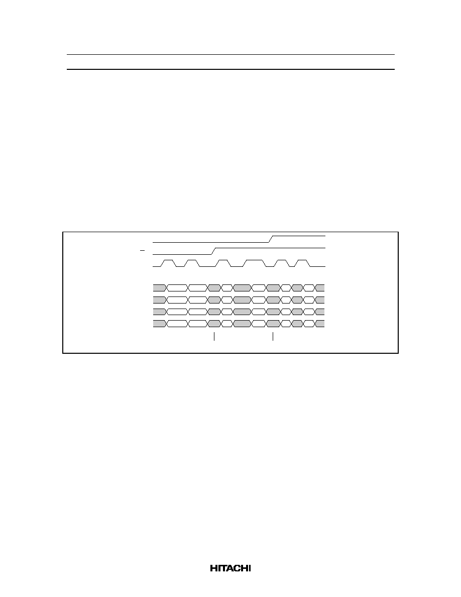
Transferring Serial Data
When the IM pin (interface mode) is low, the HD66712 enters serial interface mode. A three-line clock-
synchronous transfer method is used. The HD66712 receives serial input data (SID) and transmits serial
output data (SOD) by synchronizing with a transfer clock (SCLK) sent from the master side.
When the HD66712 interfaces with several chips, chip select pin (CS*) must be used. The transfer clock
(SCLK) input is activated by making chip select (CS*) low. In addition, the transfer counter of the
HD66712 can be reset and serial transfer synchronized by making chip select (CS*) high.
Here, since the data which was being sent at reset is cleared, restart the transfer from the first bit of this
data. In the case of a minimum 1 to 1 transfer system with the HD66712 used as a receiver only, an
interface can be established by the transfer clock (SCLK) and serial input data (SID). In this case, chip
select (CS*) should be fixed to low.
The transfer clock (SCLK) is independent from operational clock (CLK) of the HD66712. However,
when several instructions are continuously transferred, the instruction execution time determined by the
operational clock (CLK) (see continuous transfer) must be considered since the HD66712 does not have
an internal transmit/receive buffer.
To begin with, transfer the start byte. By receiving five consecutive bits (synchronizing bit string) at the
beginning of the start byte, the transfer counter of the HD66712 is reset and serial transfer is
synchronized. The 2 bits following the synchronizing bit string (5 bits) specify transfer direction (R/
:
bit) and register select (RS bit). Be sure to transfer 0 in the 8th bit.
After receiving the start byte, instructions are received and the data/busy flag is transmitted. When the
transfer direction and register select remain the same, data can be continuously transmitted or received.
The transfer protocol is described in detail below.
∑
Receiving (write)
After receiving the start synchronization bits, the R/
: bit (= 0), and the RS bit with the start byte, an
8-bit instruction is received in 2 bytes: the lower 4 bits of the instruction are placed in the LSB of the
first byte, and the higher 4 bits of the instruction are placed in the LSB of the second byte. Be sure to
transfer 0 in the following 4 bits of each byte. When instructions are continuously received with R/
:
bit and RS bit unchanged, continuous transfer is possible (see "Continuous Transfer" below).
HD66712U
401
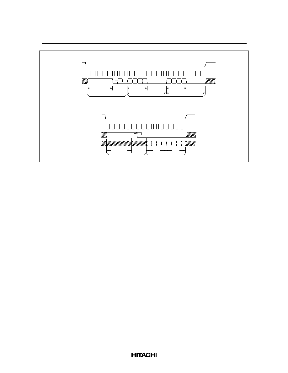
1
2
3
4
5
6
7
8
9
10
11
12
13
14
15
16
1
2
3
4
5
6
7
8
9
10
11
12
13
14
15
16
17 18
19
20
21
22
23
24
1
1
1
1
1
R/W RS
0
D0 D1 D2 D3
0
0
0
0
D4 D5 D6
D7
0
0
0
0
Starting byte
Instruction
a) Basic transfer serial data input (receive)
CS
*
(input)
SCLK
(input)
SID
(input)
CS
*
(input)
SCLK
(input)
SID
(input)
SOD
(output)
Synchronizing
bit string
Lower
data
Upper
data
1st byte
2nd byte
b) Basic transfer of serial data output (transmit)
Synchronizing
bit string
Lower
data
Upper
data
Starting byte
Busy flag/data read
1
1
1
1
1
R/W RS
0
0
0
0
0
0
0
0
0
D0 D1 D2 D3 D4 D5 D6 D7
Figure 14 Basic Procedure for Transferring Serial Data

HD66712U
402
∑
Transmitting (read)
After receiving the start synchronization bits, the R/
: bit (= 1), and the RS bit with the start byte, 8-
bit read data is transmitted in the same way as receiving. When read data is continuously transmitted
with R/
: bit and RS bit unchanged, continuous transfer is possible (see "Continuous Transfer"
below).
Even at the time of the transmission (the data output), since the HD66712 monitors the start
synchronization bit string ("11111") by the SID input, the HD66712 receives the R/W bit and RS bit
after detecting the start synchronization. Therefore, in the case of a continuous transfer, fix the SID
input "0."
∑
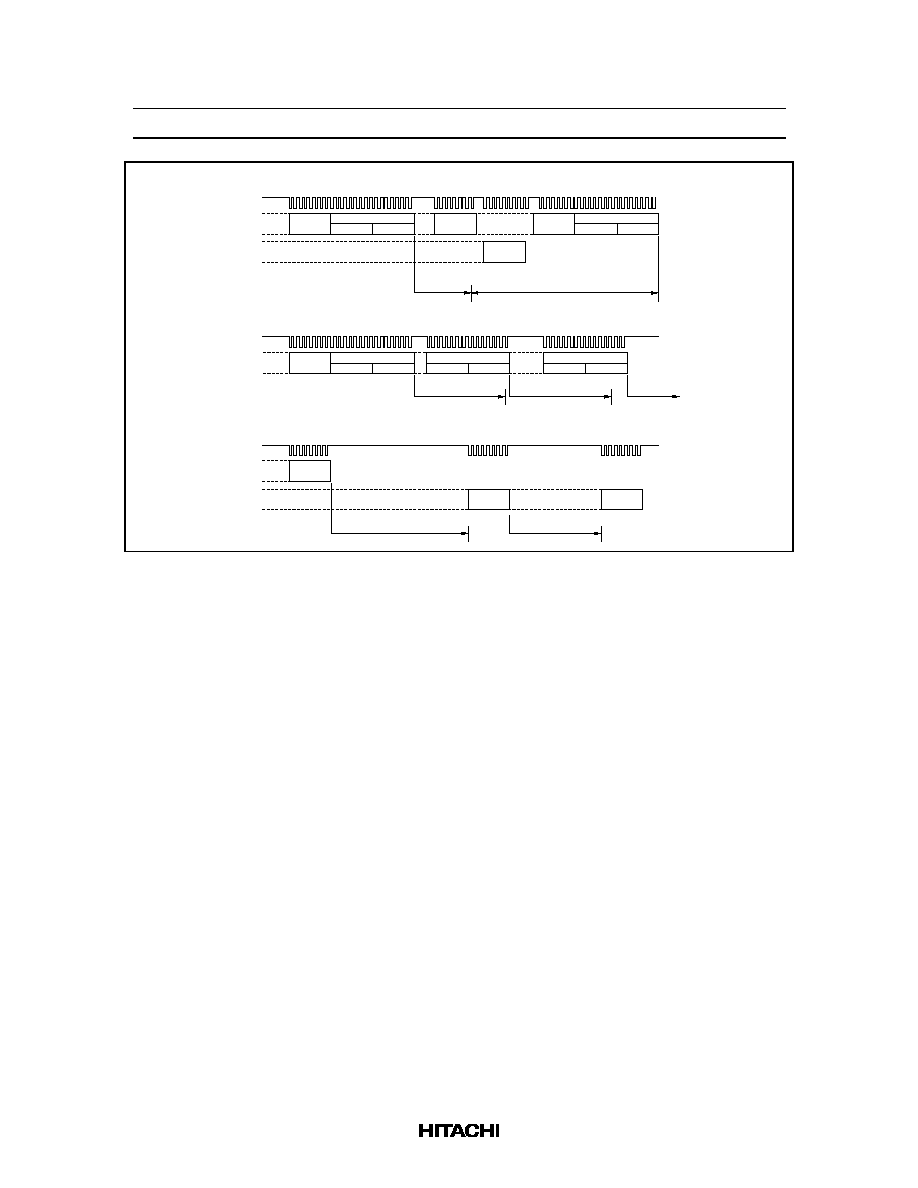
Continuous transfer
When instructions are continuously received with the R/
: bit and RS bit unchanged, continuous
receive is possible without inserting a start byte between instructions.
After receiving the last bit (the 8th bit in the 2nd byte) of an instruction, the system begins to execute
it.
To execute the next instruction, the instruction execution time of the HD66712 must be considered. If
the last bit (the 8th bit in the 2nd byte) of the next instruction is received during execution of the
previous instruction, the instruction will be ignored.
In addition, if the next unit of data is read before read execution of previous data is completed for
busy flag/address counter/RAM data, normal data is not sent. To transfer data normally, the busy flag
must be checked. However, it is possible to transfer without reading the busy flag if wiring for
transmission (SOD pin) needs to be reduced or if the burden of polling on the MPU needs to be
removed. In this case, insert a transfer wait so that the current instruction first completes execution
during instruction transfer.
HD66712U
403
Start
byte
Instruction (1)
1st byte
2nd byte
Instruction (2)
1st byte
2nd byte
Start
byte
Start
byte
Instruction (1)
1st byte
2nd byte
Instruction (3)
1st byte
2nd byte
Instruction (2)
1st byte
2nd byte
Start
byte
Busy
read
Instruction (1)
Execution
time
Instruction waiting time (not busy state)
Instruction (1)
Execution time
Instruction (2)
Execution time
Instruction (3)
Execution time
Wait
Wait
Wait
Wait
Start
byte
Data
read (1)
Data
read (2)
Instruction (1)
Execution time
Instruction (2)
Execution time
SCLK
(input)
SID
(input)
SOD
(output)
SCLK
(input)
SID
(input)
SCLK
(input)
SID
(input)
SOD
(output)
i) Continuous data write by boring processing
ii) Continuous data write by CPU wait insert
iii) Continuous data read by CPU wait insert
Figure 15 Procedure for Continuous Data Transfer

HD66712U
404
Instructions
Outline
Only the instruction register (IR) and the data register (DR) of the HD66712 can be controlled by the
MPU. Before starting internal operation of the HD66712, control information is temporarily stored in
these registers to allow interfacing with various MPUs, which operate at different speeds, or various
peripheral control devices. The internal operation of the HD66712 is determined by signals sent from the
MPU. These signals, which include register selection (RS), read/write (R/
:), and the data bus (DB0 to
DB7), make up the HD66712 instructions (Table 12). There are four categories of instructions that:
∑
Designate HD66712 functions, such as display format, data length, etc.
∑
Set internal RAM addresses
∑
Perform data transfer with internal RAM
∑
Perform miscellaneous functions
Normally, instructions that perform data transfer with internal RAM are used the most. However, auto-
incrementation by 1 (or auto-decrementation by 1) of internal HD66712 RAM addresses after each data
write can lighten the program load of the MPU. Since the display shift instruction (Table 10) can perform
concurrently with display data write, the user can minimize system development time with maximum
programming efficiency.
When an instruction is being executed for internal operation, no instruction other than the busy
flag/address read instruction can be executed.
Because the busy flag is set to 1 while an instruction is being executed, check it to make sure it is 0
before sending another instruction from the MPU.
Note:
Be sure the HD66712 is not in the busy state (BF = 1) before sending an instruction from the
MPU to the HD66712. If an instruction is sent without checking the busy flag, the time between
the first instruction and next instruction will take much longer than the instruction time itself.
Refer to Table 12 for the list of each instruction execution time.

HD66712U
405
Instruction Description
Clear Display
Clear display writes space code (20)H (character pattern for character code (20)H must be a blank
pattern) into all DDRAM addresses. It then sets DDRAM address 0 into the address counter, and returns
the display to its original status if it was shifted. In other words, the display disappears and the cursor or
blinking goes to the left edge of the display (in the first line if 2 lines are displayed). It also sets I/D to 1
(increment mode) in entry mode. S of entry mode does not change.
Return Home
Return home sets DDRAM address 0 into the address counter, and returns the display to its original status
if it was shifted. The DDRAM contents do not change.
The cursor or blinking goes to the left edge of the display (in the first line if 2 lines are displayed). In
addition, flicker may occur in a moment at the time of this instruction issue.
Entry Mode Set
I/D: Increments (I/D = 1) or decrements (I/D = 0) the DDRAM address by 1 when a character code is
written into or read from DDRAM.
The cursor or blinking moves to the right when incremented by 1 and to the left when decremented by 1.
The same applies to writing and reading of CGRAM and SEGRAM.
S: Shifts the entire display either to the right (I/D = 0) or to the left (I/D = 1) when S is 1 during DDRAM
write. The display does not shift if S is 0.
If S is 1, it will seem as if the cursor does not move but the display does. The display does not shift when
reading from DDRAM. Also, writing into or reading out from CGRAM and SEGRAM does not shift the
display. In a low power mode (LP = 1), do not set S = 1 because the whole display does not normally
shift.
Display On/Off Control
When extension register enable bit (RE) is 0, bits D, C, and B are accessed.
D: The display is on when D is 1 and off when D is 0. When off, the display data remains in DDRAM,
but can be displayed instantly by setting D to 1.
C: The cursor is displayed when C is 1 and not displayed when C is 0. Even if the cursor disappears, the
function of I/D or other specifications will not change during display data write. The cursor is displayed
using 5 dots in the 8th line for 5
◊
8 dot character font.
HD66712U
406
B: The character indicated by the cursor blinks when B is 1. The blinking is displayed as switching
between all blank dots and displayed characters at a speed of 370-ms intervals when f
cp
or f
OSC
is 270 kHz.
The cursor and blinking can be set to display simultaneously. (The blinking frequency changes according
to f
OSC
or the reciprocal of f
cp
. For example, when f
cp
is 300 kHz, 370
◊
270/300 = 333 ms.)
Extended Function Set
When the extended register enable bit (RE) is 1, FW, B/W, and NW bit shown below are accessed.
Once these registers are accessed, the set values are held even if the RE bit is set to zero.
FW: When FW is 1, each displayed character is controlled with a 6-dot width. The user font in CGRAM
is displayed with a 6-bit character width from bits 5 to 0. As for fonts stored in CGROM, no display area
is assigned to the left most bit, and the font is displayed with a 5-bit character width. If the FW bit is
changed, data in DDRAM and CGRAM SEGRAM is destroyed. Therefore, set FW before data is written
to RAM. When font width is set to 6 dots, the frame frequency decreases to 5/6 compared to 5-dot time.
See "Oscillator Circuit" for details.
B/W: When B/W is 1, the character at the cursor position is cyclically displayed with black-white
inversion. At this time, bits C and B in display on/off control register are "Don't care." When f
CP
or f
OSC
is
270 kHz, display is changed by switching every 370 ms.
NW: When NW is 1, 4-line display is performed. At this time, bit N in the function set register is "Don't
care."
i) Cursor display example
ii) Blink display example
White-black inverting
display example
iii)
Alternating
display
Alternating
display
i) 5-dot character width
ii) 6-dot character width
a) Cursor blink width control
b) Font width control
Figure 16 Example of Display Control

HD66712U
407
Cursor or Display Shift
Cursor or display shift shifts the cursor position or display to the right or left without writing or reading
display data (Table 10). This function is used to correct or search the display. In a 2-line display, the
cursor moves to the second line when it passes the 40th digit of the first line. In a 4-line display, the
cursor moves to the second line when it passes the 20th character of the line. Note that, all line displays
will shift at the same time. When the displayed data is shifted repeatedly each line moves only
horizontally. The second line display does not shift into the first line position. When this instruction is
executed, extended register enable bit (RE) is reset.
The address counter (AC) contents will not change if the only action performed is a display shift. In low
power mode (LP = 1), whole-display shift cannot be normally performed.
Scroll Enable
When extended register enable bit (RE) is 1, scroll enable bits can be set.
This HSE resister specifies scrolled line with the scroll quantity register. This register consists of 4 bits
for each display line, so a specified line can be shifted by dot unit. When the bit 0 of HSE is 1 in four line
mode (NW = 1), the first line can be shifted, and the bit 1 is specified to shift the second line, the bit 2 is
specified for the third line, and bit 3 is specified for the fourth line. When it shifts the first line in two line
mode (N = 1, NW = 0), both the bit 0 and bit 1 should be set to 1. The bit 2 and bit 3 is specified for the
second line.
In 1 line mode (N = 0, NW = 0), the bit 0 and bit 1 should be specified.
Function Set
Only when the extended register enable bit (RE) is 1, the BE and the LP bits shown below can be
accessed. Bits DL and N can be accessed regardless of RE.
DL: Sets the interface data length. Data is sent or received in 8-bit lengths (DB7 to DB0) when DL is 1,
and in 4-bit lengths (DB7 to DB4) when DL is 0. When 4-bit length is selected, data must be sent or
received twice.
N: When bit NW in the extended function set is 0, a 1- or a 2-line display is set. When N is 0, 1-line
display is selected; when N is 1, 2-line display is selected. When NW is 1, a 4-line display is set. At this
time, N is "Don't care."
Note:
After changing the N or NW or LP bit, please issue the Return Home or Clear Display instruction
to cancel to shift display.

HD66712U
408
RE: When bit RE is 1, bit BE in the extended function set register, the SEGRAM address set register,
and the function set register can be accessed. When bit RE is 0, the registers described above cannot be
accessed, and the data in these registers is held.
To maintain compatibility with the HD44780, the RE bit should be fixed to 0.
Table 10
Shift Function
S/C
R/L
0
0
Shifts the cursor position to the left. (AC is decremented by one.)
0
1
Shifts the cursor position to the right. (AC is incremented by one.)
1
0
Shifts the entire display to the left. The cursor follows the display shift.
1
1
Shifts the entire display to the right. The cursor follows the display shift.
BE: When the RE bit is 1, this bit can be rewritten. When this bit is 1, the user font in CGRAM and the
segment in SEGRAM can be blinked according to the upper two bits of CGRAM and SEGRAM.
LP: When bit RE is 1, this bit can be rewritten. When LP is set to 1 and the EXT pin is low (without an
extended driver), the HD66712 operates in low power mode. In 1-line display mode, the HD66712
operates on a 4-division clock, and in a 2-line or a 4-line display mode, the HD66712 operates on a 2-
division clock. According to these operations, instruction execution takes four times or twice as long.
Note that in low power mode, display shift cannot be performed. The frame frequency is reduced to 5/6
that of normal operation. See "Oscillator Circuit" for details.
Note:
Perform the DL, N, NW, and FW fucntions at the head of the program before executing any
instructions (except for the read busy flag and address instruction). From this point, if bits N,
NW, or FW are changed after other instructions are executed, RAM contents may be broken.
Set CGRAM Address
A CGRAM address can be set while the RE bit is cleared to 0.
Set CGRAM address into the address counter displayed by binary AAAAAA. After this address set, data
is written to or read from the MPU for CGRAM.
Set SEGRAM Address
Only when the extended register enable (RE) bit is 1, HS2 to HS0 and the SEGRAM address can be set.
The SEGRAM address in the binary form AAAA is set to the address counter. After this address set,
SEGRAM can be written to or read from by the MPU.

HD66712U
409
Set DDRAM Address
A DDRAM address can be set while the RE bit is cleared to 0. Set DDRAM address sets the DDRAM
address binary AAAAAAA into the address counter.
After this address set, data is written to or read from the MPU for DDRAM.
However, when N and NW is 0 (1-line display), AAAAAAA can be (00)H to (4F)H. When N is 1 and
NW is 0 (2-line display), AAAAAAA is (00)H to (27)H for the first line, and (40)H to (67)H for the
second line. When NW is 1 (4-line display), AAAAAAA is (00)H to (13)H for the first line, (20)H to
(33)H for the second line, (40)H to (53)H for the third line, and (60)H to (73)H for the fourth line.
Set Scroll Quantity
When extended registor enable bit (RE) is 1, HDS5 to HDS0 can be set.
HDS5 to HDS0 specifies horizontal scroll quantity to the left of the display in dot units. The HD66712
uses the unused DDRAM area to execute a desired horizontal smooth scroll from 1 to 48 dots.
Note:
When performing a horizontal scroll as described above by connecting an extended driver, the
maximum number of characters per line decreases by the quantity set by the above horizontal
scroll. For example, when the maximum 24-dot scroll quantity (4 characters) is used with 6-dot
font width and 4-line display, the maximum numbers of characters is 20 ≠ 4 = 16. Notice that in
low power mode (LP = 1), display shift and scroll cannot be performed.
Read Busy Flag and Address
Read busy flag and address reads the busy flag (BF) indicating that the system is now internally operating
on a previously received instruction. If BF is 1, the internal operation is in progress. The next instruction
will not be accepted until BF is reset to 0. Check the BF status before the next write operation. At the
same time, the value of the address counter in binary AAAAAAA is read out. This address counter is
used by both CG, DD, and SEGRAM addresses, and its value is determined by the previous instruction.
The address contents are the same as for CGRAM, DDRAM, and SEGRAM address set instructions.
Write Data to CG, DD, or SEGRAM
This instruction writes 8-bit binary data DDDDDDDD to CG, DD or SEGRAM. CG, DD or SEGRAM is
selected by the previous specification of the address set instruction (CGRAM address set / DDRAM
address set / SEGRAM address set). After a write, the address is automatically incremented or
decremented by 1 according to the entry mode. The entry mode also determines the display shift
direction.

HD66712U
410
Read Data from CG, DD, or SEG RAM
This instruction reads 8-bit binary data DDDDDDDD from CG, DD, or SEGRAM. CG, DD or SEGRAM
is selected by the previous specification of the address set instruction. If no address is specified, the first
data read will be invalid. When executing serial read instructions, the next address is normally read from
the next address. An address set instruction need not be executed just before this read instruction when
shifting the cursor by a cursor shift instruction (when reading from DDRAM). A cursor shift instruction is
the same as a set DDRAM address instruction.
After a read, the entry mode automatically increases or decreases the address by 1. However, a display
shift is not executed regardless of the entry mode.
Note:
The address counter (AC) is automatically incremented or decremented after write instructions to
CG, DD or SEGRAM. The RAM data selected by the AC cannot be read out at this time even if
read instructions are executed. Therefore, to read data correctly, execute either an address set
instruction or a cursor shift instruction (only with DDRAM), or alternatively, execute a
preliminary read instruction to ensure the address is correctly set up before accessing the data.
Table 11
HS5 to HS0 Settings
HDS5 HDS4 HDS3 HDS2 HDS1 HDS0 Description
0
0
0
0
0
0
No shift
0
0
0
0
0
1
Shift the display position to the left by one dot.
0
0
0
0
1
0
Shift the display position to the left by two dots.
0
0
0
0
1
1
Shift the display position to the left by three dots.
.
.
.
1
0
1
1
1
1
Shift the display position to the left by forty-seven dots.
1
1
*
*
*
*
Shift the display position to the left by forty-eight dots.

HD66712U
411
Table 12
Instructions
RE
Code
Execution
Time (max)
(when f
cp
or
f
OSC
is
Instruction Bit
RS
R/
:
:
DB7 DB6 DB5 DB4 DB3
DB2
DB1
DB0
Description
270 kHz)
Clear
display
0/1
0
0
0
0
0
0
0
0
0
1
Clears entire display and
sets DDRAM address 0
in address counter.
1.52 ms
Return
home
0/1
0
0
0
0
0
0
0
0
1
--
Sets DDRAM address 0
IN address counter. Also
returns display from
being shifted to original
position. DDRAM
contents remain
unchanged.
1.52 ms
Entry
mode set
0/1
0
0
0
0
0
0
0
1
I/D
S
Sets cursor move
direction and specifies
display shift. These
operations are
performed during data
write and read.
37 µs
Display
on/off
control
0
0
0
0
0
0
0
1
D
C
B
Sets entire display (D)
on/off, cursor on/off (C),
and blinking of cursor
position character (B).
37 µs
Extension
function set
1
0
0
0
0
0
0
1
FW
B/W
NW
Sets a font width, a
black-white inverting
cursor (B/W), and a 4-
line display (NW).
37 µs
Cursor or
display shift
0
0
0
0
0
0
1
S/C
R/L
--
--
Moves cursor and shifts
display without changing
DDRAM contents.
37 µs
Scroll
enable
1
0
0
0
0
0
1
HSE
HSE
HSE
HSE
Specifies which display
lines to undergo
horizontal smooth scroll.
37 µs
Function
set
0
0
0
0
0
1
DL
N
RE
--
--
Sets interface data
length(DL), number of
display lines (L), and
extension register write
enable (RE).
37 µs
1
0
0
0
0
1
DL
N
RE
BE
LP
Sets CGRAM/SEGRAM
blinking enable (BE), and
power-down mode (LP).
LP is available when the
EXT pin is low.
37 µs
Set
CGRAM
address
0
0
0
0
1
ACG ACG ACG
ACG
ACG
Ay
Sets CGRAM address.
CGRAM data is sent and
received after this
setting.
37 µs
Set
SEGRAM
address set
1
0
0
0
1
*
*
ASEG ASEG ASEG ASEG Sets SEGRAM address.
SEGRAM data is sent
and received after this
setting.
37 µs

HD66712U
412
Table 12
Instructions (cont)
RE
Code
Execution
Time (max)
(when f
cp
or
f
OSC
is
Instruction Bit
RS
R/
:
:
DB7 DB6 DB5 DB4 DB3
DB2
DB1
DB0
Description
270 kHz)
Set
DDRAM
address
0
0
0
1
ADD ADD ADD ADD
ADD
ADD
ADD
Sets DDRAM address.
DDRAM data is sent and
received after this
setting.
37 µs
Set scroll
quantity
1
0
0
1
*
HDS HDS HDS
HDS
HDS
HDS
Sets horizontal dot scroll
quantity.
37 µs
Read busy
flag &
address
0/1
0
1
BF
AC
AC
AC
AC
AC
AC
AC
Reads busy flag (BF)
indicating internal
operation is being
performed and reads
address counter
contents.
0 µs
Write data
to RAM
0/1
1
0
Write data
Writes data into
DDRAM, CGRAM, or
SEGRAM.
7 µs
t
ADD
= 5.5 µs*
Read data
from RAM
0/1
1
1
Read data
Reads data from
DDRAM, CGRAM, or
SEGRAM.
37 µs
t
ADD
= 5.5 µs*
I/D
= 1: Increment
I/D
= 0: Decrement
S
= 1: Accompanies display shift
D
= 1: Display on
C
= 1: Cursor on
B
= 1: Blink on
FW = 1: 6-dot font width
B/W = 1: Black-white inverting cursor on
NW = 1: Four lines
NW = 0: One or two lines
S/C = 1: Display shift
S/C = 0: Cursor move
R/L = 1: Shift to the right
R/L = 0: Shift to the left
DL
= 1: 8 bits, DL = 0: 4 bits
N
= 1: 2 lines, N = 0: 1 line
RE
= 1: Extension register access enable
BE
= 1: CGRAM/SEGRAM blinking enable
LP
= 1: Low-power mode
BF
= 1: Internally operating
BF
= 0:
Instructions acceptable
DDRAM:
Display data RAM
ADD:
DDRAM address
(corresponds
to cursor address)
CGRAM:
Character generator RAM
ACG:
CGRAM address
SEGRAM: Segment RAM
ASEG:
Segment RAM address
HSE:
Specifies horizontal scroll
lines
HDS:
Horizontal dot scroll
quantity
AC:
Address counter used for
both DD, CG, and
SEGRAM addresses.
Note:
1. -- indicates no effect.
* After execution of the CGRAM/DDRAM data write or read instruction, the RAM address
counter is incremented or decremented by 1. The RAM address counter is updated after the
busy flag turns off. In Figure 17, t
ADD
is the time elapsed after the busy flag turns off until the
address counter is updated.
2. Extension time changes as frequency changes. For example, when f is 300 kHz, the execution
time is: 37 µs
◊
270/300 = 33 µs.
3. Execution time in a low-power mode (LP = 1 and EXT = low) becomes four times for a 1-line
mode, and twice for a 2- or 4-line mode.
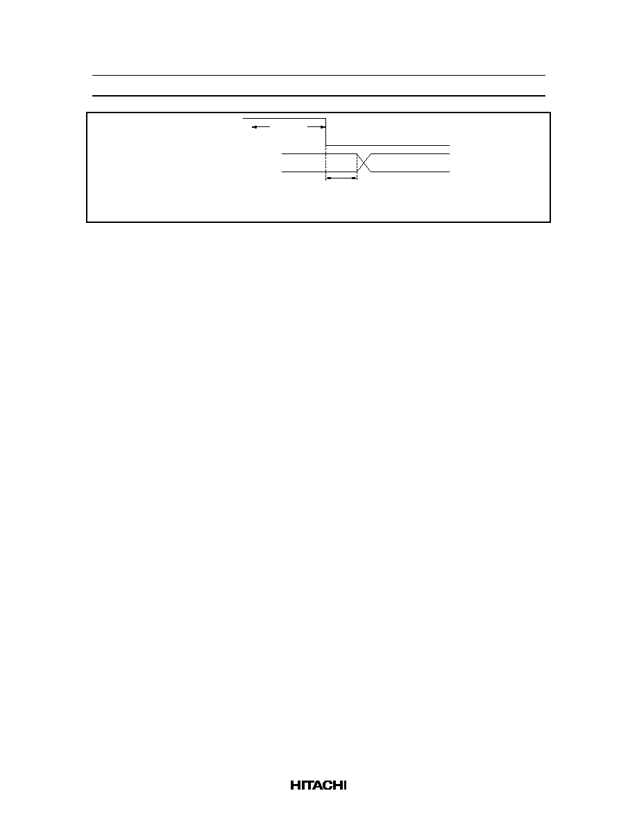
HD66712U
413
Busy state
Busy state
(DB7 pin)
Address counter
(DB0 to DB6 pins)
t
ADD
A
A + 1
t depends on the operation frequency.
t = 1.5/(f or f ) seconds
ADD
ADD
cp
OSC
Figure 17 Address Counter Update
HD66712U
414
Interfacing the HD66712
Interface with 8-Bit MPUs: The HD66712 can interface directly with an 8-bit MPU using the E clock,
or with an 8-bit MCU through an I/O port.
When the number of I/O ports in the MCU, or the interfacing bus width, if limited, a 4-bit interface
function is used.
R/W
E
Internal
signal
DB7
Internal operation
Data
Busy
Busy
Not
Busy
Data
Instruction
write
Busy flag check
Busy flag check Busy flag check
Instruction
write
RS
Figure 18 Example of 8-Bit Data Transfer Timing Sequence
C0
C1
C2
A0≠A7
E
RS
R/W
DB0≠DB7
8
H8/325
I/O port interface
HD66712
Figure 19 8-Bit MPU Interface
HD66712U
415
Interface with 4-Bit MPUs: The HD66712 can interface with a 4-bit MCU through an I/O port. 4-bit
data representing high and low order bits must be transferred sequentially.
The DL bit in function-set selects 4-bit or 8-bit interface data length.
E
Internal
signal
DB7
Internal operation
Instruction
write
Busy flag check
Busy flag check
Instruction
write
RS
IR7
Busy
Not
Busy
IR3
AC3
AC3
D7
D3
R/W
Figure 20 Example of 4-Bit Data Transfer Timing Sequence
D15
D14
D13
R10≠R13
RS
R/W
E
DB4≠DB7
HMCS4019R
HD66712
4
Figure 21 4-bit MPU Interface
HD66712U
416
Oscillator Circuit
OSC1
OSC1
OSC2
Clock
Rf
The oscillator frequency can be
adjusted by oscillator resistance
(Rf). If Rf is increased or power
supply voltage is decreased, the
oscillator frequency decreases.
The recommended oscillator
resistor is as follows.
HD66712
∑ Rf = 91 k
±
2% (V
CC
= 5V)
∑ Rf = 75 k
±
2% (V
CC
= 3V)
∑ Rf = 130 k
±
2% (V
CC
= 5V)
∑ Rf = 110 k
±
2% (V
CC
= 3V)
1) When an external clock is used
2) When an internal oscillator is used
HD66712
i) HD66712S
ii) HD66712U
Figure 22 Oscillator Circuit
1
2
3
4
32
33
1
2
3
32
33
V
CC
V1
V4
V5
COM1
1-line selection period
(2) 1 /33 duty cycle
1 frame
1 frame
1
2
3
4
16
17
1
2
3
16
17
1-line selection period
V
CC
V1
V4
V5
COM1
1 frame
1 frame
(1) 1 /17 duty cycle
Item
Line selection period
Frame frequency
Normal Display Mode (LP = 0)
5-Dot Font Width
Low Power Mode (LP = 1)
5-Dot Font Width
200 clocks
79.4 Hz
240 clocks
66.2 Hz
60 clocks
66.2 Hz
72 clocks
55.1 Hz
Item
Line selection period
Frame frequency
Normal Display Mode (LP = 0)
Low Power Mode (LP = 1)
100 clocks
81.8 Hz
120 clocks
68.2 Hz
60 clocks
68.2 Hz
72 clocks
56.8 Hz
6-Dot Font Width
6-Dot Font Width
5-Dot Font Width
5-Dot Font Width
6-Dot Font Width
6-Dot Font Width
Note: At the calculation example above for displayed frame frequency, all oscillator frequencies are
270 kHz (1 clock = 3.7
µ
s).
Note: At the calculation example above for displayed frame frequency, all oscillator frequencies are
270 kHz (1 clock = 3.7
µ
s).
Figure 23 Frame Frequency
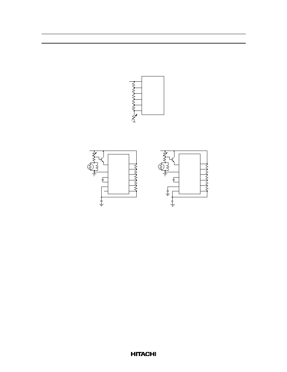
HD66712U
417
Power Supply for Liquid Crystal Display Drive
1) When an external power supply is used
V
CC
V1
V2
V3
V4
V5
V
CC
R
R
R0
R
R
VR
V
EE
2) When an internal booster is used
V
CC
V1
V2
V3
V4
V5
V
CC
C1
C2
Vci
GND
V5OUT2
R
R
R0
R
R
C1
C2
Vci
GND
V5OUT2
R
R
R0
R
R
V5OUT3
V5OUT3
µ
1 F
+
µ
1 F
+
µ
1 F
+
µ
1 F
+
µ
1 F +
(Boosting twice)
(Boosting three times)
V
CC
V1
V2
V3
V4
V5
V
CC
Notes: 1.
2.
3.
Boosting output voltage should not exceed the power supply voltage (2) (13V max.)
in the absolute maximum ratings. Especially, voltage of over 4.3V should not be input
to the reference voltage (Vci) when boosting three times.
Vci input terminal is used for reference voltage and power supply for the internal booster.
Input current into the Vci pin needs three times or more of load current through the
bleeder resistor for LCD. So, when it adjusts LCD driving voltage (Vlcd), input voltage
should be controlled with transistor to supply LCD load current. Please notice
connection (+/≠) when it uses capacitors with poler.
The Vci must be set below the power supply (V
CC
).
NTC-type
thermistor
NTC-type
thermistor
GND
GND
GND
GND
HD66712U
418
Table 13
Duty Factor and Power Supply for Liquid Crystal Display Drive
Item
Data
Number of Lines
1
2, 4
Duty factor
1/17
1/33
Bias
1/5
1/6.7
Divided resistance
R
R
R
R0
R
2.7R
Note: R changes depending on the size of liquid crystal panel. Normally, R must be 4.7 k
to 20 k
.
HD66712U
419
Extension Driver LSI Interface
By bringing the EXT pin high, extended driver interface signals (CL1, CL2, D, and M) are output.
Table 14
Relationships between the Number of Display Lines and 40-Output Extension Driver
Controller
HD66712
HD66710
HD44780
HD66702
Display Lines
5-Dot Width 6-Dot Width
5-Dot Width 6-Dot Width
5-Dot Width
5-Dot Width
16
◊
2 lines
Not required Not required
Not required 1
1
Not required
20
◊
2 lines
Not required Not required
1
1
2
Not required
24
◊
2 lines
Not required 1
1
2
2
1
40
◊
2 lines
Disabled
Disabled
Disabled
Disabled
4
3
12
◊
4 lines
Not required 1
1
1
Disabled
Disabled
16
◊
4 lines
1
1
1
2
Disabled
Disabled
20
◊
4 lines
1
2
2
3
Disabled
Disabled
Note: The number of display lines can be extended to 32
◊
2 lines or 20
◊
4 lines in the LCD-II/F12.
The number of display lines can be extended to 30
◊
2 lines or 20
◊
4 lines in the LCD-II/F8.
COM0≠
COM33
SEG1≠SEG60
EXT
SEG1≠
SEG60
GND
HD66712
COM0≠
COM33
EXT
CL1
V
CC
CL2
M
D
CL1
HD66712
SEG1≠
SEG60
Extension driver
Seg1≠
Seg40
CL2 D
M
a) 1-chip operation
(EXT = Low, 5-dot font width)
b) When using the extension driver
(EXT = High, 5-dot font width)
24
◊
2-line display
32
◊
2-line display
Figure 24 HD66712 and the Extension Driver Connection
HD66712U
420
Table 15
Display Start Address in Each Mode
Number of Lines
1-Line Mode
2-Line Mode
4-Line Mode
Output
5 Dot
6 Dot
5 Dot
6 Dot
5 Dot/6 Dot
COM1≠COM8
D00±1
D00±1
D00±1
D00±1
D00±1
COM9≠COM16
D0C±1
D0A±1
D0C±1
D0A±1
D20±1
COM17≠COM24
--
--
D40±1
D40±1
D40±1
COM25≠COM32
--
--
D4C±1
D4A±1
D60±1
COM0/COM17
S00
S00
--
--
--
COM0/COM33
--
--
S00
S00
S00
Notes: 1. The number of display lines is determined by setting the N/NW bit. The font width is
determined by the FW bit.
2. D** is the start address of display data RAM (DDRAM).
3. S** is the start address of segment RAM (SEGRAM).
4. ±1 following D** indicates increment or decrement at display shift.
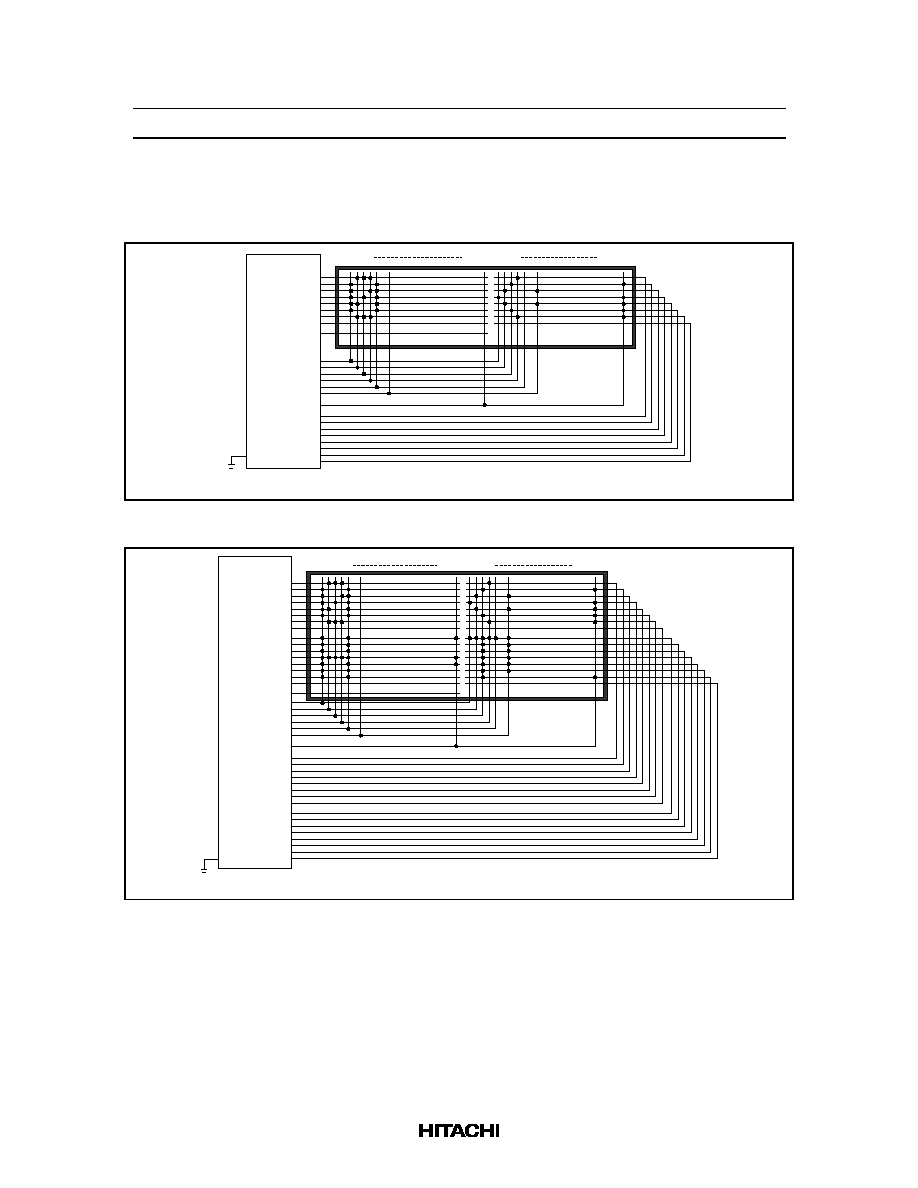
HD66712U
421
Interface to Liquid Crystal Display
∑
Example of 5-dot font width connection
COM1
COM2
COM3
COM4
COM5
COM6
COM7
COM8
COM9
COM10
COM11
COM12
COM13
COM14
COM15
COM16
SEG1
SEG2
SEG3
SEG4
SEG5
SEG60
COM17
(COM0)
HD66712
1
12
13
24
SEG6
EXT
±
+ ≠ x
˜
=
Note: COM0 and COM17 output the same signals. Apply them according to the wiring pattern.
Figure 25 24
◊
◊
1-Line + 60-Segment Display (5-Dot Font, 1/17 Duty)
HD66712
COM1
COM2
COM3
COM4
COM5
COM6
COM7
COM8
COM17
COM18
COM19
COM20
COM21
COM22
COM23
COM24
COM9
COM10
COM11
COM12
COM13
COM14
COM15
COM16
COM25
COM26
COM27
COM28
COM29
COM30
COM31
COM32
SEG1
SEG2
SEG3
SEG4
SEG5
SEG60
COM33
(COM0)
1
12
13
24
SEG6
EXT
±
+ ≠ x
˜
=
Note: COM0 and COM33 output the same signals. Apply them according to the wiring pattern.
Figure 26 24
◊
◊
1-Line + 60-Segment Display (5-Dot Font, 1/33 Duty)
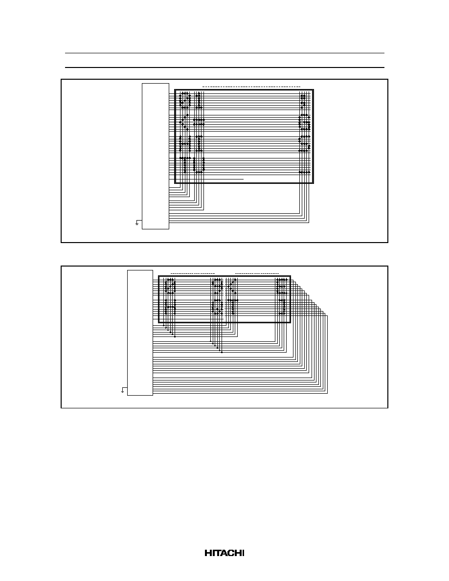
HD66712U
422
HD66712
COM1
COM2
COM3
COM4
COM5
COM6
COM7
COM8
COM9
COM10
COM11
COM12
COM13
COM14
COM15
COM16
COM56
COM57
COM58
COM59
SEG1
SEG2
SEG3
SEG4
SEG5
SEG6
SEG7
SEG8
SEG9
SEG10
1
2
12
EXT
COM17
COM18
COM19
COM20
COM21
COM22
COM23
COM24
COM25
COM26
COM27
COM28
COM29
COM30
COM31
COM32
±
+ ≠ x
˜
=
COM60
COM33
(COM0)
Note: COM0 and COM33 output the same signals. Apply them according to the wiring pattern.
Figure 27 12
◊
◊
4-Line + 60 Segment Display (5-Dot Font, 1/33 Duty)
HD66712
COM1
COM2
COM3
COM4
COM5
COM6
COM7
COM8
COM17
COM18
COM19
COM20
COM21
COM22
COM23
COM24
COM9
COM10
COM11
COM12
COM13
COM14
COM15
COM16
COM25
COM26
COM27
COM28
COM29
COM30
COM31
COM32
SEG1
SEG2
SEG3
SEG4
SEG5
SEG55
SEG56
SEG57
SEG58
SEG59
COM33
(COM0)
SEG6
SEG60
EXT
1
10
11
20
±
+ ≠ x
˜
=
Note: COM0 and COM33 output the same signals. Apply them according to the wiring pattern.
Figure 28 20
◊
◊
2-Line + 60 Segment Display (6-Dot Font, 1/33 Duty)

HD66712U
423
Instruction and Display Correspondence
∑
8-bit operation, 24-digit
◊
1-line display with internal reset
Refer to Table 16 for an example of an 24-digit
◊
1-line display in 8-bit operation. The HD66712
functions must be set by the function set instruction prior to the display. Since the display data RAM
can store data for 80 characters, a character unit scroll can be performed by a display shift instruction.
A dot unit smooth scroll can also be performed by a horizontal scroll instruction. Since data of display
RAM (DDRAM) is not changed by a display shift instruction, the display can be returned to the first
set display when the return home operation is performed.
∑
4-bit operation, 24-digit
◊
1-line display with internal reset
The program must set all functions prior to the 4-bit operation (see Table 17.) When the power is
turned on, 8-bit operation is automatically selected and the first write is performed as an 8-bit
operation. Since DB0 to DB3 are not connected, a rewrite is then required. However, since one
operation is completed in two accesses for 4-bit operation, a rewrite is needed to set the functions.
Thus, DB4 to DB7 of the function set instruction is written twice.
∑
8-bit operation, 24-digit
◊
2-line display with internal reset
For a 2-line display, the cursor automatically moves from the first to the second line after the 40th
digit of the first line has been written. Thus, if there are only 16 characters in the first line, the
DDRAM address must be again set after the 16th character is completed. (See Table 18.)
The display shift is performed for the first and second lines. If the shift is repeated, the display of the
second line will not move to the first line. The same display will only shift within its own line for the
number of times the shift is repeated.
∑
8-bit operation, 12-digit
◊
4-line display with internal reset
The RE bit must be set by the function set instruction and then the NW bit must be set by an
extension function set instruction. In this case, 4-line display is always performed regardless of the N
bit setting (see Table 19).
In a 4-line display, the cursor automatically moves from the first to the second line after the 20th digit
of the first line has been written. Thus, if there are only 8 characters in the first line, the DDRAM
address must be set again after the 8th character is completed. Display shifts are performed on all
lines simultaneously.
Note:
When using the internal reset, the electrical characteristics in the Power Supply Conditions Using
Internal Reset Circuit Table must be satisfied. If not, the HD66712 must be initialized by
instructions. See the section, Initializing by Instruction.
HD66712U
424
Table 16
8-Bit Operation, 24-Digit
◊
◊
1-Line Display Example with Internal Reset
Step
Instruction
No.
RS
R/
:
:
DB7 DB6 DB5 DB4 DB3 DB2 DB1 DB0 Display
Operation
1
Power supply on (the HD66712 is initialized by the internal reset
circuit)
Initialized. No display.
2
Function set
0
0
0
0
1
1
0
0
*
*
Sets to 8-bit operation and
selects 1-line display.
Bit 2 must always be cleared.
3
Return home
0
0
0
0
0
0
0
0
1
0
Return both display and cursor
to the original position(address
0).
4
Display on/off control
0
0
0
0
0
0
1
1
1
0
_
Turns on display and cursor.
Entire display is in space mode
because of initialization.
5
Entry mode set
0
0
0
0
0
0
0
1
1
0
_
Sets mode to increment the
address by one and to shift the
cursor to the right at the time of
write to the RAM. Display is not
shifted.
6
Write data to CGRAM/DDRAM
1
0
0
1
0
0
1
0
0
0
H_
Writes H. DDRAM has already
been selected by initialization
when the power was turned on.
7
Write data to CGRAM/DDRAM
1
0
0
1
0
0
1
0
0
1
HI_
Writes I.
8
∑
∑
∑
∑
∑
∑
∑
∑
∑
∑
9
Write data to CGRAM/DDRAM
1
0
0
1
0
0
1
0
0
1
HITACHI_
Writes I.
10
Entry mode set
0
0
0
0
0
0
0
1
1
1
HITACHI_
Sets mode to shift display at the
time of write.
11
Write data to CGRAM/DDRAM
1
0
0
0
1
0
0
0
0
0
ITACHI _
Writes a space.
HD66712U
425
Table 16
8-Bit Operation, 24-Digit
◊
◊
1-Line Display Example with Internal Reset (cont)
Step
Instruction
No.
RS
R/
:
:
DB7 DB6 DB5 DB4 DB3 DB2 DB1 DB0 Display
Operation
12
Write data to CGRAM/DDRAM
1
0
0
1
0
0
1
1
0
1
TACHI M_
Writes M.
13
∑
∑
∑
∑
∑
∑
∑
∑
∑
14
Write data to CGRAM/DDRAM
1
0
0
1
0
0
1
1
1
1
MICROKO_
Writes O.
15
Cursor or display shift
0
0
0
0
0
1
0
0
*
*
MICROKO
_
Shifts only the cursor position to
the left.
16
Cursor or display shift0
0
0
0
0
1
0
0
*
*
MICROKO
_
Shifts only the cursor position to
the left.
17
Write data to CGRAM/DDRAM
1
0
0
1
0
0
0
0
1
1
ICROCO
_
Writes C over K.
The display moves to the left.
18
Cursor or display shift
0
0
0
0
0
1
1
1
*
*
MICROCO
_
Shifts the display and cursor
position to the right.
19
Cursor or display shift
0
0
0
0
0
1
0
1
*
*
MICROCO_
Shifts the display and cursor
position to the right.
20
Write data to CGRAM/DDRAM
1
0
0
1
0
0
1
1
0
1
ICROCOM_
Writes M.
21
∑
∑
∑
∑
∑
∑
∑
∑
∑
∑
22
Return home
0
0
0
0
0
0
0
0
1
0
HITACHI
_
Returns both display and cursor
to the original position (address
0).
HD66712U
426
Table 17
4-Bit Operation, 24-Digit
◊
◊
1-Line Display Example with Internal Reset
Step
Instruction
No.
RS
R/
:
:
DB7 DB6 DB5 DB4 DB3 DB2 DB1 DB0 Display
Operation
1
Power supply on (the HD66712 is initialized by
the internal reset circuit)
Initialized. No display.
2
Function set
0
0
0
0
1
0
--
--
--
--
--
--
--
--
--
--
--
--
--
--
Sets to 4-bit operation. Clear bit
2. In this case, operation is
handled as 8 bits by
initialization. *
1
3
Function set
0
0
0
0
1
0
--
--
--
--
0
0
0
1
0
0
--
--
--
--
Sets 4-bit operation and
selects1-line display. Clear BE,
LP bits. 4-bit operation starts
from this step.
4
Function set
0
0
0
0
1
0
--
--
--
--
0
0
0
0
*
*
--
--
--
--
Sets 4-bit operation and
selects1 line display. Clear bit 2
(RE).
5
Return home
0
0
0
0
0
0
--
--
--
--
0
0
0
0
1
0
--
--
--
--
Returns both display and cursor
to the original position (address
0).
6
Display on/off control
0
0
0
0
0
0
--
--
--
--
0
0
1
1
1
0
--
--
--
--
_
Turns on display and cursor.
Entire display is in space mode
because of initialization.
7
Entry mode set
0
0
0
0
0
0
--
--
--
--
0
0
0
1
1
0
--
--
--
--
_
Sets mode to increment the
address by one and to shift the
cursor to the right at the time of
write to the DD/CGRAM.
Display is not shifted.
8
Write data to CGRAM/DDRAM
1
0
0
1
0
0
--
--
--
--
1
0
1
0
0
0
--
--
--
--
H_
Writes H.
DDRAM has already been
selected by initialization.
9
∑
∑
∑
∑
∑
∑
∑
∑
∑
∑
Based on 8-bit operation after
this instruction
Note:
The control is the same as for 8-bit operation beyond step #8.
1. When DB3 to DB0 pins are open in 4-bit mode, the RE, BE, LP bits are set to "1" at step #2.
So, these bits are clear to "0" at step #3.

HD66712U
427
Table 18
8-Bit Operation, 24-Digit
◊
◊
2-Line Display Example with Internal Reset
Step
Instruction
No.
RS
R/
:
:
DB7 DB6 DB5 DB4 DB3 DB2 DB1 DB0 Display
Operation
1
Power supply on (the HD66712 is initialized by the internal reset
circuit)
Initialized. No display.
2
Function set
0
0
0
0
1
1
1
0
*
*
Sets to 8-bit operation and
selects 2-line display.
Clear bit 2.
3
Display on/off control
0
0
0
0
0
0
1
1
1
0
_
Turns on display and cursor. All
display is in space mode
because of initialization.
4
Entry mode set
0
0
0
0
0
0
0
1
1
0
_
Sets mode to increment the
address by one and to shift the
cursor to the right at the time of
write to the RAM. Display is not
shifted.
5
Write data to CGRAM/DDRAM
1
0
0
1
0
0
1
0
0
0
H_
Writes "H." DDRAM has already
been selected by initialization at
power-on.
6
∑
∑
∑
∑
∑
∑
∑
∑
∑
∑
7
Write data to CGRAM/DDRAM
1
0
0
1
0
0
1
0
0
1
HITACHI_
Writes I.
8
Set DDRAM address
0
0
1
1
0
0
0
0
0
0
HITACHI
_
Sets DDRAM address so that
the cursor is positioned at the
head of the second line.

HD66712U
428
Table 18
8-Bit Operation, 24-Digit
◊
◊
2-Line Display Example with Internal Reset (cont)
Step
Instruction
No.
RS
R/
:
:
DB7 DB6 DB5 DB4 DB3 DB2 DB1 DB0 Display
Operation
9
Write data to CGRAM/DDRAM
1
0
0
1
0
0
1
1
0
1
HITACHI
M_
Writes a space.
10
∑
∑
∑
∑
∑
∑
∑
∑
∑
∑
11
Write data to CGRAM/DDRAM
1
0
0
1
0
0
1
1
1
1
HITACHI
MICROCO_
Writes O.
12
Entry mode set
0
0
0
0
0
0
0
1
1
1
HITACHI
MICROCO_
Sets mode to shift display at the
time of write.
13
Write data to CGRAM/DDRAM
1
0
0
1
0
0
1
1
0
1
ITACHI
ICROCOM_
Writes M.
14
∑
∑
∑
∑
∑
∑
∑
∑
∑
∑
17
Return home
0
0
0
0
0
0
0
0
1
0
HITACHI
MICROCOM
_
Returns both display and cursor
to the original position (address
0).
HD66712U
429
Table 19
8-Bit Operation, 12-Digit
◊
◊
4-Line Display Example with Internal Reset
Step
Instruction
No.
RS
R/
:
:
DB7 DB6 DB5 DB4 DB3 DB2 DB1 DB0 Display
Operation
1
Power supply on (the HD66712 is initialized by the internal reset
circuit)
Initialized. No display.
2
Function set
0
0
0
0
1
1
1
1
*
*
Sets 8-bit operation and enables
write to the extension register.
3
4-line mode set
0
0
0
0
0
0
1
0
0
1
Sets 4-line operation.
4
Function set
Inhibit write to extension register
0
0
0
0
1
1
0
0
*
*
Inhibits write to extension
register. Invalidates selection of
1-line/2-line by bit 3.
5
Display on/off control
0
0
0
0
0
0
1
1
1
0
_
Turns on display and cursor.
Entire display is cleared
because of initialization.
6
Entry mode set
0
0
0
0
0
0
0
1
1
0
_
Sets mode to increment the
address by one and to shift the
cursor to the right when writing
to RAM. Display is not shifted.
7
Write data to CGRAM/DDRAM
1
0
0
1
0
0
1
0
0
0
_
Writes H. DDRAM has already
been selected by initialization.
8
∑
∑
∑
∑
∑
∑
∑
∑
∑
∑

HD66712U
430
Table 19
8-Bit Operation, 12-Digit
◊
◊
4-Line Display Example with Internal Reset (cont)
Step
Instruction
No.
RS
R/
:
:
DB7 DB6 DB5 DB4 DB3 DB2 DB1 DB0 Display
Operation
9
Write data to CGRAM/DDRAM
1
0
0
1
0
0
1
0
0
1
HITACHI_
Writes I.
10
Set DDRAM address
0
0
1
0
1
0
0
0
0
0
HITACHI
_
Sets DDRAM address to (20)H
so that the cursor is positioned
at the beginning of the second
line.
11
Write data to CGRAM
1
0
0
0
1
1
0
0
0
0
HITACHI
0_
Writes 0.
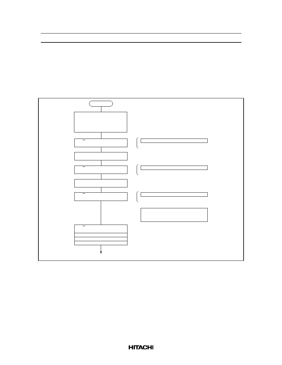
HD66712U
431
Initializing by Instruction
If the power supply conditions for correctly operating the internal reset circuit are not met, initialization
by instructions becomes necessary.
∑
Initializing when a length of interface is 8-bit system. (See Figure 29.)
∑
Initializing when a length of interface is 4-bit system. (See Figure 30.)
Power on
Wait for more than 4.1 ms
Wait for more than 100
µ
s
RS
0
R/W
0
DB7
0
DB6
0
DB5
1
DB4
1
DB3 DB2 DB1 DB0
*
*
*
*
RS
0
R/W
0
DB7
0
DB6
0
DB5
1
DB4
1
DB3 DB2 DB1 DB0
*
*
*
*
RS
0
R/W
0
DB7
0
DB6
0
DB5
1
DB4
1
DB3 DB2 DB1 DB0
*
*
*
*
RS
0
R/W
0
DB7
0
DB6
0
DB5
1
DB4
1
DB3
N
DB2
0
DB1 DB0
*
*
0
0
0
0
0
0
0
0
0
0
0
0
0
0
0
0
0
0
1
0
0
0
0
1
0
0
I/D
0
1
S
Initialization ends
BF cannot be checked before this instruction.
Function set (Interface is 8 bits long.)
BF cannot be checked before this instruction.
Function set (Interface is 8 bits long.)
BF cannot be checked before this instruction.
Function set (Interface is 8 bits long.)
BF can be checked after the following instructions.
When BF is not checked, the waiting time between
instructions is longer than the execution instruction
time. (See Table 12.)
Function set
Display off
Display clear
Entry mode set
∑ Wait for more than 15 ms
after V
CC
rises to 4.5V
(V
CC
= 5V during operation)
∑ Wait for more than 40 ms
after V
CC
rises to 2.7V
(V
CC
= 3V during operation)
Figure 29 Initializing Flow of 8-Bit Interface

HD66712U
432
Initialization ends
∑ Wait for more than 15 ms
after V
CC
rises to 4.5V
(V
CC
= 5V during operation)
∑ Wait for more than 40 ms
after V
CC
rises to 2.7V
(V
CC
= 3V during operation)
BF cannot be checked before this instruction.
Function set (Interface is 8 bits long)
BF cannot be checked before this instruction.
Function set (Interface is 8 bits long)
BF cannot be checked before this instruction.
Function set (Interface is 8 bits long)
DB7
0
DB6
0
DB5
1
DB4
1
RS
0
R/W
0
Wait for more than 4.1 ms
DB7
0
DB6
0
DB5
1
DB4
1
RS
0
R/W
0
Wait for more than 100
µ
s
DB7
0
DB6
0
DB5
1
DB4
1
RS
0
R/W
0
DB7
0
DB6
0
DB5
1
DB4
0
RS
0
R/W
0
0
N
0
N
0
1
0
0
0
0
0
1
0
0
0
0
0
0
0
1
1
0
1
*
0
0
0
0
0
I/D
0
0
0
*
0
0
0
1
0
S
0
0
0
0
0
0
0
0
0
0
0
0
0
0
0
0
0
0
0
0
BF can be checked after the following instructions.
When BF is not checked, the waiting time between
instructions is longer than the execution instruction
time. (See Table 12.)
*
1
Function set (4-bit mode)
Display off
Display clear
Entry mode set (I/D, S specification)
Function set (4-bit mode, N specification)
BE, LP are clear to 0
Power on
Function set (4-bit mode, N specification)
*
1
*
1
*
2
Important Notice
When DB3 to DB0 pins are open in 4-bit mode,
the N, RE, BE, LP bits are set to "1." In this case,
instruction time becomes four times in a low
power mode (LP = "1").
The low power mode is available in this step, so
instruction time takes four times.
Notes: 1.
2.
Figure 30 Initializing Flow of 4-Bit Interface

HD66712U
433
Horizontal Dot Scroll
Dot unit scrolls are performed by setting the horizontal dot scroll quantity resister (HDS) when the
extension register is enabled (RE = "1"). And the shifted line can be selected with the scroll enable
register (HDE). So, it can control dot unit shifts by each display line.
To scroll smoothly, HD66712 supports 6 dots-font width mode (FW = 1). The below figures are examples
of scroll display.
No shift performed
One dot shift to the left
When 5-dots font width (FW = 0)
Two dots shift to the left
Three dots shift to the left
Four dots shift to the left
When 6-dots font width (FW = 1)
No shift performed
One dot shift to the left
Two dots shift to the left
Three dots shift to the left
Four dots shift to the left
Five dots shift to the left
ICON mark and 1st to 3rd line are fixed,
and only 4th line is sifted
HDS = 1000
(4th line scroll enable)
Example of 10 digits
◊
4 lines with 6-dots fonts width mode
Figure 31 Example of Dot Scroll Display
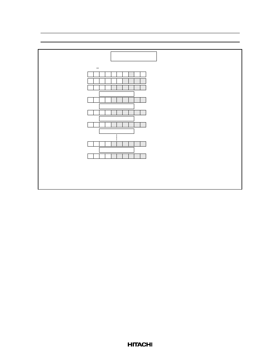
HD66712U
434
DB7 DB6 DB5 DB4 DB3 DB2 DB1 DB0
RS R/W
0
0
0
0
1
DL
N
1
BE LP
Enable extension resistor.
1
4th line scroll enable.
One dot shift in 4th line to the left.
Two dots shift in 4th line to the left.
Three dots shift in 4th line to the left.
CPU Wait
CPU Wait
CPU Wait
Four dots shift in 4th line to the left.
CPU Wait
0
0
1
0
0
0
0
0
0
1
3
0
0
0
0
0
1
1
0
0
0
2
0
0
1
0
0
0
0
0
1
0
4
0
0
1
0
0
0
0
0
1
1
5
0
0
1
0
0
0
0
1
0
0
6
47 dots shift in 4th line to the left.
CPU Wait
48 dots shift in 4th line to the left.
0
0
1
1
1
0
1
1
1
1
49
0
0
1
0
1
1
0
0
0
0
50
Note:
When perfoming a dot scroll with an extended driver, the maximum number or characters
per line decreases by quantity set by the dot scroll. For example, when the maximum
24-dot scroll quantity (4 characters) is used with 6-dot font width and 4-line display,
the maximum numbers of character is 20 ≠ 4 = 16. Notice that in low power mode (LP = 1),
display shift and dot scroll cannot be performed.
6-dots font width mode (FW = 1)
4 line display mode (NW = 1)
Figure 32 Method of Smooth Scroll Display
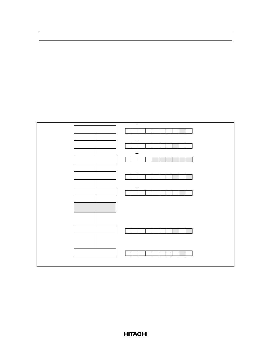
HD66712U
435
Low Power Mode
When the extension driver is not used (EXT = Low) with extension register enabled (RE = 1), the
HD66712 enters low power mode by setting the low-power mode bit (LP) to 1. During low-power mode,
as the internal operation clock is divided by 2 (2-line/4-line display mode) or by 4 (1-line display mode),
the execution time of each instruction becomes two times or four times longer than normal. In addition,
as the frame frequency decreases to 5/6, display quality might be affected.
In addition, since the display is not shifted in low power mode, display shift must be cleared with the
return home instruction before setting low power mode. The amount of horizontal scroll must also be
cleared (HDS = 000000). Moreover, because the display enters a shift state after clearing low-power
mode, the home return instruction must be used to clear display shift at that time.
RS R/W DB7 DB6 DB5 DB4 DB3 DB2 DB1 DB0
0
0
0
0
0
0
0
0
0
RS R/W
R/W
DB7 DB6 DB5 DB4 DB3 DB2 DB1 DB0
0
0
0
0
1
DL
N
BE
0
RS
DB7 DB6 DB5 DB4 DB3 DB2 DB1 DB0
0
0
1
0
0
0
0
RS R/W DB7 DB6 DB5 DB4 DB3 DB2 DB1 DB0
0
0
0
0
1
DL
N
BE
RS R/W DB7 DB6 DB5 DB4 DB3 DB2 DB1 DB0
0
0
0
0
1
DL
N
BE
Note: The execution time of an instruction in low-power
mode becomes two times or four times longer
then normal. The frame frequency also
decreases by 5/6.
Return home
Extended register enable
Return home
Clear horizontal scroll quantity
HDS = 000000
Set a low power mode
Clear low power mode
Low power operation
1
1
1
1
0
0
0
1
0
RS R/W DB7 DB6 DB5 DB4 DB3 DB2 DB1 DB0
0
0
0
0
0
0
0
0
0
Return home
1
Note: Up until this instruction, execution time is two
times or four times longer than normal.
Note: Because the display enters a shift state, be sure
to execute this instruction.
RS R/W DB7 DB6 DB5 DB4 DB3 DB2 DB1 DB0
0
0
0
0
0
0
0
1
0
0
Figure 33 Usage of Low Power Mode
HD66712U
436
Absolute Maximum Ratings*
Item
Symbol
Unit
Value
Notes
Power supply voltage (1)
V
CC
V
≠0.3 to +7.0
1
Power supply voltage (2)
V
CC
≠V5
V
≠0.3 to +13.0
1, 2
Input voltage
Vt
V
≠0.3 to V
CC
+0.3
1
Operating temperature
T
opr
∞C
≠20 to +75
Storage temperature
T
stg
∞C
≠55 to +125
4
Note:
*
If the LSI is used above these absolute maximum ratings, it may become permanently
damaged. Using the LSI within the following electrical characteristic limits is strongly
recommended for normal operation. If these electrical characteristic conditions are also
exceeded, the LSI will malfunction and cause poor reliability.

HD66712U
437
DC Characteristics (V
CC
= 2.7V to 5.5V, T
a
= ≠20 to +75∞C*
3
)
Item
Symbol
Min
Typ
Max
Unit
Test Condition
Notes*
Input high voltage (1)
(except OSC1)
VIH1
0.7V
CC
--
V
CC
V
6
Input low voltage (1)
VIL1
≠0.3
--
0.2V
CC
V
V
CC
= 2.7 to 3.0V
6
(except OSC1)
≠0.3
--
0.6
V
V
CC
= 3.0 to 4.5V
Input high voltage (2)
(OSC1)
VIH2
0.7V
CC
--
V
CC
V
15
Input low voltage (2)
(OSC1)
VIL2
--
--
0.2V
CC
V
15
Output high voltage (1)
(D0≠D7)
VOH1
0.75V
CC
--
--
V
≠I
OH
= 0.1 mA
7
Output low voltage (1)
(D0≠D7)
VOL1
--
--
0.2V
CC
V
I
OL
= 0.1 mA
7
Output high voltage (2)
(except D0≠D7)
VOH2
0.8V
CC
--
--
V
≠I
OH
= 0.04 mA
8
Output low voltage (2)
(except D0≠D7)
VOL2
--
--
0.2V
CC
V
I
OL
= 0.04 mA
8
Driver ON resistance
(COM)
R
COM
--
2
20
k
±Id = 0.05 mA
(COM)
VLCD = 4V
13
Driver ON resistance
(SEG)
R
SEG
--
2
30
k
±Id = 0.05 mA
(SEG)
VLCD = 4V
13
I/O leakage current
I
LI
≠1
--
1
µA
VIN = 0 to V
CC
9
Pull-up MOS current
(D0≠D7, RESET* pin)
≠Ip
10
50
120
µA
V
CC
= 3V
VIN = 0V
Current
consumption
Normal
display
I
CC
--
130
300
µA
R
f
oscillation
external clock
10, 14
(HD66712U) LP mode1
(1/33duty)
I
LP1
--
90
--
µA
V
CC
= 3V
f
osc
= 270 kHz
LP mode2
(1/17duty)
I
LP2
--
65
--
µA
LCD voltage
VLCD1
2.7
--
11.0
V
V
CC
≠V5, 1/5 bias
16
VLCD2
2.7
--
11.0
V
V
CC
≠V5, 1/6.7 bias
16
Note:
*
Refer to Electrical Characteristics Notes following these tables.

HD66712U
438
Booster Characteristics
Item
Symbol
Min
Typ
Max
Unit
Test Condition
Notes*
Output voltage
(V5OUT2 pin)
VUP2
7.5
8.7
--
V
Vci = 4.5V, I
0
= 0.25 mA,
C = 1 µF, f
OSC
= 270 kHz
T
a
= 25∞C
18, 19
Output voltage
(V5OUT3 pin)
VUP3
7.0
7.7
--
V
Vci = 2.7V, I
0
= 0.25 mA,
C = 1 µF, f
OSC
= 270 kHz
T
a
= 25∞C
18, 19
Input voltage
VCi
1.0
--
5.0
V
Vci
V
CC
T
a
= 25∞C
18, 19
Note:
*
Refer to Electrical Characteristics Notes following these tables.
AC Characteristics (V
CC
= 2.7V to 5.5V, T
a
= ≠20 to +75∞C*
3
)
Clock Characteristics (V
CC
= 2.7V to 5.5V, T
a
= ≠20 to +75∞C*
3
)
Item
Symbol
Min
Typ
Max
Unit
Test Condition Notes*
External
External clock frequency
f
cp
125
270
410
kHz
11
clock
External clock duty
Duty
45
50
55
%
operation
External clock rise time
t
rcp
--
--
0.2
µs
External clock fall time
t
rcp
--
--
0.2
µs
R
f
oscillation
Clock oscillation frequency f
OSC
190
270
350
kHz
R
f
= 130 k
,
V
CC
= 5V
HD66712U
12
Note:
*
Refer to the Electrical Characteristics Notes section following these tables.

HD66712U
439
System Interface Timing Characteristics (1) (V
CC
= 2.7V to 4.5V, T
a
= ≠20 to
+75∞C*
3
)
Bus Write Operation
Item
Symbol Min
Typ
Max
Unit
Test Condition
Enable cycle time
t
cycE
1000
--
--
ns
Figure 34
Enable pulse width (high level)
PW
EH
450
--
--
Enable rise/fall time
t
Er
, t
Ef
--
--
25
Address set-up time (RS, R/W to E)
t
AS
60
--
--
Address hold time
t
AH
20
--
--
Data set-up time
t
DSW
195
--
--
Data hold time
t
H
10
--
--
Bus Read Operation
Item
Symbol Min
Typ
Max
Unit
Test Condition
Enable cycle time
t
cycE
1000
--
--
ns
Figure 35
Enable pulse width (high level)
PW
EH
450
--
--
Enable rise/fall time
t
Er
, t
Ef
--
--
25
Address set-up time (RS, R/W to E)
t
AS
60
--
--
Address hold time
t
AH
20
--
--
Data delay time
t
DDR
--
--
360
Data hold time
t
DHR
5
--
--

HD66712U
440
Serial Interface Operation
Item
Symbol
Min
Typ
Max
Unit
Test Condition
Serial clock cycle time
t
SCYC
1
--
20
µs
Figure 36
Serial clock (high level width)
t
SCH
400
--
--
ns
Serial clock (low level width)
t
SCL
400
--
--
Serial clock rise/fall time
t
SCr
, t
SCf
--
--
50
Chip select set-up time
t
CSU
60
--
--
Chip select hold time
t
CH
200
--
--
Serial input data set-up time
t
SISU
200
--
Serial input data hold time
t
SIH
200
--
--
Serial output data delay time
t
SOD
--
--
360
Serial output data hold time
t
SOH
0
--
--
HD66712U
441
System Interface Timing Characteristics (2) (V
CC
= 4.5V to 5.5V, T
a
= ≠20 to
+75∞C*
3
)
Bus Write Operation
Item
Symbol Min
Typ
Max
Unit
Test Condition
Enable cycle time
t
cycE
500
--
--
ns
Figure 34
Enable pulse width (high level)
PW
EH
230
--
--
Enable rise/fall time
t
Er
, t
Ef
--
--
20
Address set-up time (RS, R/W to E)
t
AS
40
--
--
Address hold time
t
AH
10
--
--
Data set-up time
t
DSW
80
--
--
Data hold time
t
H
10
--
--
Bus Read Operation
Item
Symbol Min
Typ
Max
Unit
Test Condition
Enable cycle time
t
cycE
500
--
--
ns
Figure 35
Enable pulse width (high level)
PW
EH
230
--
--
Enable rise/fall time
t
Er
, t
Ef
--
--
20
Address set-up time (RS, R/W to E)
t
AS
40
--
--
Address hold time
t
AH
10
--
--
Data delay time
t
DDR
--
--
160
Data hold time
t
DHR
5
--
--
HD66712U
442
Serial Interface Sequence
Item
Symbol
Min
Typ
Max
Unit
Test Condition
Serial clock cycle time
t
SCYC
0.5
--
20
µs
Figure 36
Serial clock (high level width)
t
SCH
200
--
--
ns
Serial clock (low level width)
t
SCL
200
--
--
Serial clock rise/fall time
t
SCr
, t
SCf
--
--
50
Chip select set-up time
t
CSU
60
--
--
Chip select hold time
t
CH
100
--
--
Serial input data set-up time
t
SISU
100
--
--
Serial input data hold time
t
SIH
100
--
--
Serial output data delay time
t
SOD
--
--
160
Serial output data hold time
t
SOH
0
--
--
Segment Extension Signal Timing (V
CC
= 2.7V to 5.5V, T
a
= ≠20 to +75∞C*
3
)
Item
Symbol
Min
Typ
Max
Unit
Test Condition
Clock pulse width
High level
t
CWH
800
--
--
ns
Figure 37
Low level
t
CWL
800
--
--
Clock set-up time
t
CSU
500
--
--
Data set-up time
t
SU
300
--
--
Data hold time
t
DH
300
--
--
M delay time
t
DM
≠1000
--
1000
Clock rise/fall time
t
ct
--
--
100
Reset Timing (V
CC
= 2.7V to 5.5V, T
a
= ≠20 to +75∞C*
3
)
Item
Symbol
Min
Typ
Max
Unit
Test Condition
Reset low-level width
t
RES
10
--
--
ms
Figure 38
Power Supply Conditions Using Internal Reset Circuit
Item
Symbol
Min
Typ
Max
Unit
Test Condition
Power supply rise time
t
rCC
0.1
--
10
ms
Figure 39
Power supply off time
t
OFF
1
--
--
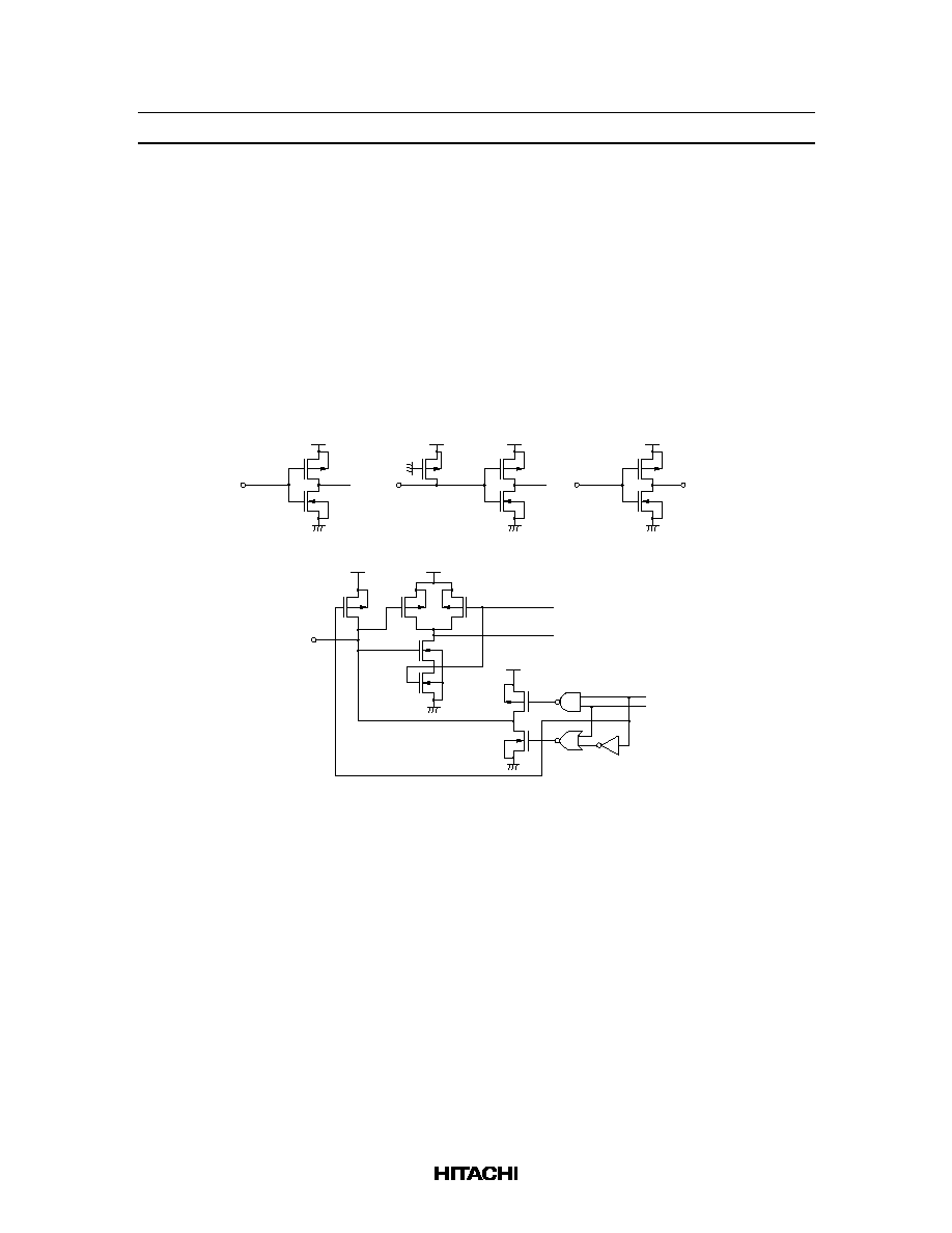
HD66712U
443
Electrical Characteristics Notes
1. All voltage values are referred to GND = 0V. If the LSI is used above the absolute maximum ratings,
it may become permanently damaged. Using the LSI within the following electrical characteristic is
strongly recommended to ensure normal operation. If these electrical characteristic are also exceeded,
the LSI may malfunction or exhibit poor reliability.
2. V
CC
V1
V2
V3
V4
V5 must be maintained.
3. For die products, specified up to 75∞C.
4. For die products, specified by the die shipment specification.
5. The following four circuits are I/O pin configurations except for liquid crystal display output.
V
CC
PMOS
NMOS
V
CC
V
CC
PMOS
NMOS
(pull-up MOS)
PMOS
V
CC
PMOS
NMOS
V
CC
NMOS
NMOS
V
CC
PMOS
NMOS
(output circuit)
(tristate)
Output enable
Data
(pull-up MOS)
I/O Pin
Pins: DB0/SOD≠DB7
(MOS with pull-up)
Input pin
Pin: E/SCLK, RS/CS
*
, RW/SID, IM,
EXT, TEST (MOS without pull-up)
Pins: RESET
*
(MOS with pull-up)
Output pin
Pins: CL1, CL2, M, D
V
CC
(input circuit)
PMOS
PMOS
Input enable
6. Applies to input pins and I/O pins, excluding the OSC1 pin.
7. Applies to I/O pins.
8. Applies to output pins.
9. Current flowing through pull-up MOSs, excluding output drive MOSs.
HD66712U
444
10. Input/output current is excluded. When input is at an intermediate level with CMOS, the excessive
current flows through the input circuit to the power supply. To avoid this from happening, the input
level must be fixed high or low.
11. Applies only to external clock operation.
Oscillator
OSC1
OSC2
0.7 V
CC
0.5 V
CC
0.3 V
CC
T
h
T
l
t
fcp
t
fcp
Duty = 100%
T
h
T
h
+ T
l
◊
Open
12. Applies only to the internal oscillator operation using oscillation resistor R
f
.
OSC1
OSC2
R
f
R :
R :
f
f
75 k
±
2% (when V = 3V to 4V)
91 k
±
2% (when V = 4V to 5V)
R
f
: 110 k
±
2% (when V
CC
= 3V to 4V)
R
f
: 130 k
±
2% (when V
CC
= 4V to 5V)
Since the oscillation frequency varies depending on the OSC1 and
OSC2 pin capacitance, the wiring length to these pins should be minimized.
CC
CC
V
CC
= 5V
400
300
270
200
50
100
150
91
130
110
R
f
(k
)
f
OSC
(kHz)
V
CC
= 3V
400
300
270
200
50
100
150
R
f
(k
)
f
OSC
(kHz)
75
Referential data
i) HD66712S
ii) HD66712U
HD66712U (typ.)
HD66712S (typ.)
HD66712U (typ.)
HD66712S (typ.)
HD66712U
445
13. R
COM
is the resistance between the power supply pins (V
CC
, V1, V4, V5) and each common signal pin
(COM0 to COM33).
R
SEG
is the resistance between the power supply pins (V
CC
, V2, V3, V5) and each segment signal pin
(SEG1 to SEG60).
14. The following graphs show the relationship between operation frequency and current consumption.
1.8
1.6
1.4
1.2
1.0
0.8
0.6
0.4
0.2
0.0
0
100
200
300
400
500
f
OSC
or f
cp
(kHz)
I
CC
(mA)
V
CC
= 5V
0.9
0.8
0.7
0.6
0.5
0.4
0.3
0.2
0.1
0.0
0
100
200
300
400
500
f
OSC
or f
cp
(kHz)
I
CC
(mA)
V
CC
= 3V
max.
typ.
max.
(normal mode)
typ.
(normal mode)
typ.
(low power mode)
15. Applies to the OSC1 pin.
16. Each COM and SEG output voltage is within ±0.15V of the LCD voltage (V
CC
, V1, V2, V3, V4, V5)
when there is no load.
17. The TEST pin must be fixed to ground, and the IM or EXT pin must also be connected to V
CC
or
ground.
18. Booster characteristics test circuits are shown below.
GND
V
CC
1
µ
F
1
µ
F
Vci
C1
C2
V5OUT2
V5OUT3
+
(Boosting three times)
+
1
µ
F
+
GND
V
CC
1
µ
F
Vci
C1
C2
V5OUT2
V5OUT3
(Boosting twice)
+
1
µ
F
+
Rload
Rload
I
O
I
O
HD66712U
446
19. Reference data
The following graphs show the liquid crystal voltage booster characteristics.
VUP2 = V
CC
≠V5OUT2
VUP3 = V
CC
≠V5OUT3
2.0
3.0
4.0
5.0
11
10
9
8
7
6
5
4
Boosting twice
V
ci
(V)
VUP2 (V)
Test condition: Vci = V
CC
, f
cp
= 270 kHz,
T
a
= 25
∞
C, Rload = 25 k
(1) VUP2, VUP3 vs Vci
2.0
3.0
4.0
5.0
15
14
13
12
11
10
9
8
7
6
Boosting three times
V
ci
(V)
VUP3 (V)
Test condition: Vci = V
CC
, f
cp
= 270 kHz,
Ta = 25
∞
C, Rload = 25 k
0.0
0.5
1.0
1.5
9.0
8.5
8.0
7.5
7.0
6.5
6.0
Boosting twice
I
o
(mA)
VUP2 (V)
Test condition: Vci
= V
CC
= 4.5V,
R
f
= 91 k
, T
a
= 25
∞
C
(2) VUP2, VUP3 vs I
o
2.0
Test condition: Vci = V
CC
= 2.7V,
R
f
= 75 k
, T
a
= 25
∞
C
8.0
7.5
7.0
6.5
6.0
5.5
5.0
Boosting three times
I
o
(mA)
VUP3 (V)
0.0
0.5
1.0
1.5
2.0
Boosting twice
(3) VUP2, VUP3 vs T
a
9.0
8.5
8.0
7.5
7.0
≠60
≠20
20
60
T
a
(
∞
C)
Test condition: Vci = V
CC
= 4.5V,
R
f
= 91 k
, I
o
= 0.25 mA
100
0
VUP2 (V)
typ.
min.
typ.
min.
typ.
min.
typ.
min.
8.0
7.5
7.0
6.5
6.0
VUP3 (V)
Boosting three times
≠60
≠20
20
60
T
a
(
∞
C)
Test condition: Vci = V
CC
= 2.7V,
R
f
= 75 k
, I
o
= 0.25 mA
100
0
typ.
typ.
HD66712U
447
Boosting twice
(4) VUP2, VUP3 vs capacitance
9.0
8.5
8.0
7.5
7.0
0.5
1.0
C (
µ
F)
Test condition: Vci = V
CC
= 4.5V,
R
f
= 91 k
, I
o
= 0.25 mA
1.5
VUP2 (V)
typ.
min.
8.0
7.5
7.0
6.5
6.0
VUP2 (V)
0.5
1.0
Test condition: Vci = V
CC
= 2.7V,
R
f
= 75 k
, I
o
= 0.25 mA
1.5
C (
µ
F)
typ.
min.
Boosting three times
20. Must maintain ("High") V
CC
Vci ("Low").

HD66712U
448
Load Circuits
AC Characteristics Test Load Circuits
Data bus: DB0≠DB7, SOD
Test
point
50 pF
Segment extension signals: CL1, CL2, D, M
30 pF
Test
point
HD66712U
449
Timing Characteristics
RS
R/W
E
DB0 to DB7
VIH1
VIL1
VIH1
VIL1
t
AS
t
AH
VIL1
VIL1
t
AH
PW
EH
t
Ef
VIH1
VIL1
VIH1
VIL1
t
Er
t
DSW
H
t
VIH1
VIL1
VIH1
VIL1
t
CYCE
VIL1
Valid data
Figure 34 Bus Write Operation
RS
R/W
E
DB0 to DB7
VIH1
VIL1
VIH1
VIL1
t
AS
t
AH
VIH1
VIH1
t
AH
PW
EH
t
Ef
VIH1
VIL1
VIH1
VIL1
t
DDR
DHR
t
t
Er
VIL1
VOH1
VOL1
VOH1
VOL1
Valid data
t
CYCE
Figure 35 Bus Read Operation
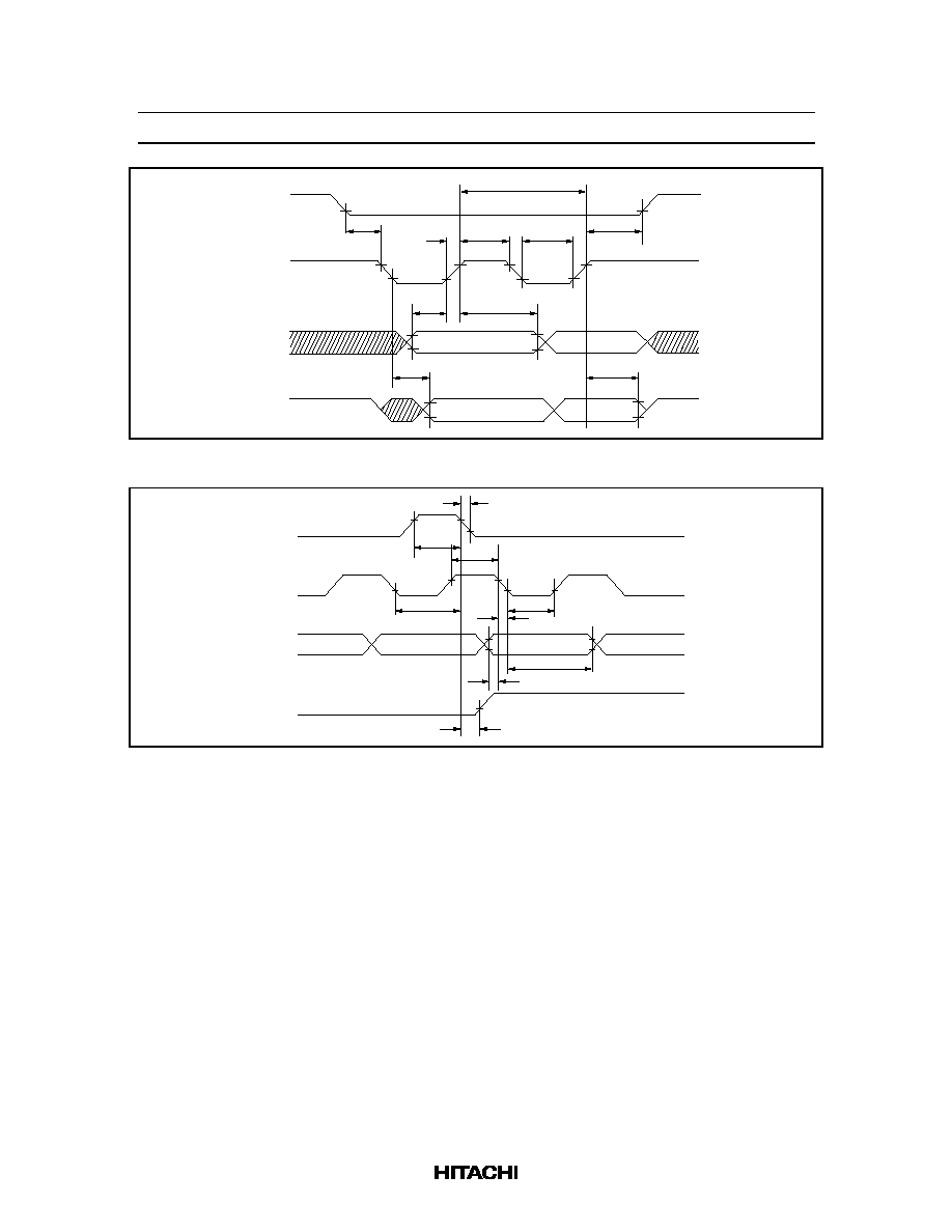
HD66712U
450
CS
*
SCLK
SID
SOD
t
SCYC
t
CSU
t
SCH
t
SCr
t
SCf
t
CWL
t
CH
t
SIH
t
SISU
t
SOH
t
SOD
VIL1
VIL1
VIH1
VIL1
VIL1
VIH1
VIL1
VIL1
VIH1
VIH1
VIL1
VIH1
VIL1
VOH1
VOL1
VOH1
VOL1
Figure 36 Serial Interface Timing
CL1
CL2
D
M
VOH2
VOH2
VOL2
t
ct
t
CWH
t
CWH
VOH2
t
CSU
t
CWL
t
ct
t
DH
t
SU
VOL2
t
DM
VOH2
VOL2
VOL2
Figure 37 Interface Timing with Extension Driver
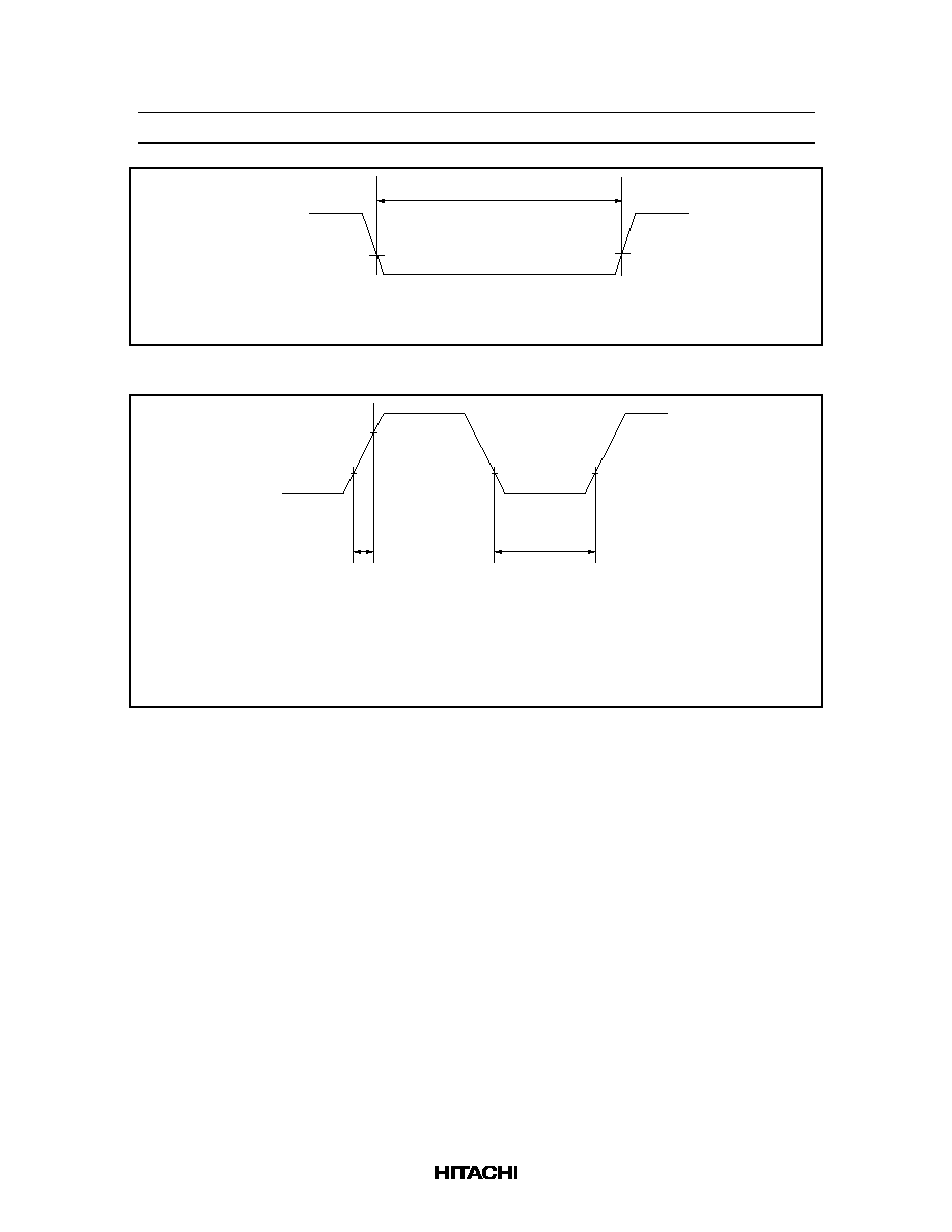
HD66712U
451
t
RES
VIL1
VIL1
RESET
*
Note: When power is supplied, initializing by the internal reset circuit has priority. Accordingly,
the above RESET
*
input is ignored during internal reset period.
Figure 38 Reset Timing
V
CC
0.2V
2.7V/4.5V
*
2
0.2V
0.2V
t
rcc
t
OFF
*
1
0.1 ms t 10 ms
rcc
t 1 ms
OFF
Notes: 1.
2.
3.
t
OFF
compensates for the power oscillation period caused by momentary power
supply oscillations.
Specified at 4.5V for 5-volt operation, and at 2.7V for 3-volt operation.
If the above electrical conditions are not satisfied, the internal reset circuit will not
operate normally. In this case, initialized by instruction. (Refer to the Initializing by
Instruction section.)
Figure 39 Power Supply Sequence