 | –≠–ª–µ–∫—Ç—Ä–æ–Ω–Ω—ã–π –∫–æ–º–ø–æ–Ω–µ–Ω—Ç: HD66720 | –°–∫–∞—á–∞—Ç—å:  PDF PDF  ZIP ZIP |

1
HD66727
(Low-Power Dot-Matrix Liquid Crystal Display Controller/Driver
with Key Scan Function)
Description
The HD66727, dot-matrix liquid crystal display controller and driver LSI incorporating a key scan
function, displays alphanumerics, katakana, hiragana, and symbols. It can be configured to drive a dot-
matrix liquid crystal display and control key scan functions under the control of an I
2
C bus or a clock-
synchronized serial microprocessor. A single HD66727 is capable of displaying up to four 12-character
lines, 40 segments, and 12 annunciators, and controlling up to a 4-by-8 key matrix, and driving three LED.
The HD66727 incorporates all the functions required for driving a dot-matrix liquid crystal display such as
display RAM, character generator, and liquid crystal drivers, and it also incorporates a booster for the LCD
power supply and key scan functions.
The HD66727 provides various functions to reduce the power consumption of an LCD system such as low-
voltage operation of 2.4V or less, a booster for generating a maximum of triple LCD drive voltage from the
supplied voltage, and voltage-followers for decreasing the direct current flow in the LCD drive bleeder-
resistors. Combining these hardware functions with software functions such as standby and sleep modes
allows a fine power control. The HD66727, with the above functions, is suitable for any portable battery-
driven product requiring long-term driving capabilities and small size.
Features
∑
Control and drive of a dot-matrix LCD with built-in key scan functions
∑
Four 12-character lines, 40 segments, and 12 annunciators
∑
Control of up to a 4
◊
8-key matrix, 3 LED ports and 3 general ports
∑
Low-power operation support:
2.4 to 5.5V (low voltage)
Double or triple booster for liquid crystal drive voltage
Contrast adjuster and voltage followers for decreasing the direct current flow in the LCD drive
bleeder-resistors
Standby mode and sleep mode
Displays up to 12 static annunciators
∑
I
2
C bus or clock-synchronized serial interface
∑
60
◊
8-bit display data RAM (60 characters max)

HD66727
2
∑
11,520-bit character generator ROM
240 characters (6
◊
8 dots)
∑
32
◊
6-bit character generator RAM
4 characters (6
◊
8 dots)
∑
8
◊
6-bit segment RAM
40 segment-icons and marks max
∑
60-segment
◊
34-common liquid crystal display driver
∑
Programmable display sizes and duty ratios (see Table 1)
∑
Vertical smooth scroll
∑
Vertical double-height display of all character fonts
∑
Horizontal double display with dedicated character fonts (6-dot font width used)
∑
Wide range of instruction functions:
Clear display, display on/off control, icon and mark control, character blink, white-black inverting
blinking cursor, icon and mark blink, return home, cursor on/off, white-black inverting raster-row
∑
Internal oscillation with an external resistor
∑
Hardware reset
∑
Wide range of LCD drive voltages
3.0V to 13.0V
∑
Slim chip with bumps for chip-on-glass (COG) mounting, slim chip without bumps for chip-on-board
(COB) mounting, and tape carrier package (TCP) (under development)
Table 1
Programmable Display Sizes and Duty Ratios
Display
Size
Duty
Ratio
Oscillation
Frequency
Current
Consumption
Multi-
plexed-
Drive
Segments
Static-
Drive
Annu-
nciators
Scanned
Keys
LED
Drive
General
Port
1 line
◊
12
characters
1/10
40 kHz
8
µ
A
40
12
32 (4
◊
8)
3
3
2 lines
◊
12
characters
1/18
80 kHz
15
µ
A
40
12
32 (4
◊
8)
3
3
3 lines
◊
12
characters
1/26
120 kHz
23
µ
A
40
12
32 (4
◊
8)
3
3
4 lines
◊
12
characters
1/34
160 kHz
30
µ
A
40
12
32 (4
◊
8)
3
3
Note:
Current consumption excludes that for LCD power supply source; V
CC
= 3V.

HD66727
3
Type Name
Type Name
External
Dimension
Operation Voltage
Internal Font
HD66727A03TA0L
TCP
2.4V to 5.5V
Japanese and European fonts
HCD66727A03
Bare chip
HCD66727A03BP
Au-bumped chip
HD66727A04TA0L
TCP
2.4V to 5.5V
PHS & Pager fonts
HCD66727A04
Bare chip
HCD66727A04BP
Au-bumped chip

HD66727
4
LCD-II Family Comparison
Item
LCD-II
(HD44780U)
HD66702R
HD66710
HD66712U
Power supply voltage
2.7V to 5.5V
5V
±
10% (standard)
2.7 V to 5.5V
(low voltage)
2.7V to 5.5V
2.7V to 5.5V
Liquid crystal drive
voltage
3.0 to 11.0V
3.0V to 8.3V
3.0 to 13.0V
2.7 to 11.0V
Maximum display -
characters per chip
8 characters
◊
2 lines
20 characters
◊
2 lines
16 characters
◊
2 lines/
8 characters
◊
4 lines
24 characters
◊
2 lines/
12 characters
◊
4 lines
Segment display
None
None
40
60 (extended to 80)
Display duty ratio
1/8, 1/11, and
1/16
1/8, 1/11, and
1/16
1/17 and 1/33
1/17 and 1/33
CGROM
9,920 bits
(208 5-
◊
-8 dot
characters and
32 5-
◊
-10 dot
characters)
7,200 bits
(160 5-
◊
-7 dot
characters and
32 5-
◊
-10 dot
characters)
9,600 bits
(240 5-
◊
-8 dot
characters)
9,600 bits
(240 5-
◊
-8 dot
characters)
CGRAM
64 bytes
64 bytes
64 bytes
64 bytes
DDRAM
80 bytes
80 bytes
80 bytes
80 bytes
SEGRAM
None
None
8 bytes
16 bytes
Segment signals
40
100
40
60
Common signals
16
16
33
34
Liquid crystal drive
waveform
A
B
B
B
Clock source
External resistor
or external clock
External resistor
or external clock
External resistor
or external clock
External resistor
or external clock
Rf oscillation frequency
270 kHz
±
30%
320 kHz
±
30%
270 kHz
±
30%
270 kHz
±
30%
Liquid crystal voltage
booster circuit
None
None
Double or triple
booster circuit
Double or triple
booster circuit
Liquid crystal drive
operational amplifier
None
None
None
None
Bleeder-resistor for liquid
crystal drive
External
External
External
External
Liquid crystal contrast
adjuster
None
None
None
None
Key scan circuit
None
None
None
None
Extension driver control
signal
Independent
control signal
Independent
control signal
Used in common
with a driver
output pin
Independent
control signal
Reset function
Internal reset
circuit
Internal reset
circuit
Internal reset
circuit
Internal reset
circuit or reset input
Horizontal smooth scroll
Impossible
Impossible
Dot unit
Dot unit and
line unit
Vertical smooth scroll
Impossible
Impossible
Impossible
Impossible
Number of displayed lines 1 or 2
1 or 2
1, 2, or 4
1, 2, or 4
Low power control
None
None
Low power mode
Low power mode
Bus interface
4 or 8 bits
4 or 8 bits
4 or 8 bits
Serial, 4, or 8 bits
Package
80-pin QFP1420
80-pin TQFP1414
80-pin bare chip
144-pin FQFP2020
144-pin bare chip
100-pin QFP1420
100-pin TQFP1414
100-pin bare chip
128-pin TCP
128-pin bare chip

HD66727
5
LCD-II Family Comparison (cont)
Item
HD66720
HD66717
HD66727
Power supply voltage
2.7V to 5.5V
2.4V to 5.5V
2.4V to 5.5V
Liquid crystal drive
voltage
3.0 to 11.0V
3.0 to 13.0V
3.0 to 13.0V
Maximum display
characters per chip
10 characters
◊
1 line/
8 characters
◊
2 lines
12 characters
◊
1 line/2 lines/3 lines/4 lines
12 characters
◊
1 line/2 lines/3 lines/4 lines
Segment display
42 (extended to 80)
40 (and 10 annunciators)
40 (and 12 annunciators)
Display duty ratio
1/9 and 1/17
1/10, 1/18, 1/26, and 1/34
1/10, 1/18, 1/26, and 1/34
CGROM
9,600 bits
(240 5-
◊
-8 dot
characters)
9,600 bits
(240 5-
◊
-8 dot
characters)
11,520 bits
(240 6-
◊
-8 dot
characters)
CGRAM
64 bytes
32 bytes
32 bytes
DDRAM
40 bytes
60 bytes
60 bytes
SEGRAM
16 bytes
8 bytes
8 bytes
Segment signals
42
60
60
Common signals
17
34
34
Liquid crystal drive
waveform
B
B
B
Clock source
External resistor
or external clock
External resistor
or external clock
External resistor
or external clock
Rf oscillation frequency
160 kHz
±
30%
1-line mode: 40 kHz
±
30%
2-line mode: 80 kHz
±
30%
3-line mode: 120 kHz
±
30%
4-line mode: 160 kHz
±
30%
1-line mode: 40 kHz
±
30%
2-line mode: 80 kHz
±
30%
3-line mode: 120 kHz
±
30%
4-line mode: 160 kHz
±
30%
Liquid crystal voltage
booster circuit
Double or triple
booster circuit
Double or triple
booster circuit
Double or triple
booster circuit
Liquid crystal drive
operational amplifier
None
Built-in for each V1 to V5
Built-in for each V1 to V5
Bleeder-resistor for liquid
crystal drive
External
Internal 1/4 and 1/6 bias
resistors
Internal 1/4 and 1/6 bias
resistors
Liquid crystal contrast
adjuster
None
Incorporated
Incorporated
Key scan circuit
5
◊
6 = 30 keys
None
4
◊
8 = 32 keys
Extension driver control
signal
Independent
control signal
None
None
Reset function
Internal reset
circuit or reset input
Reset input
Reset input
Horizontal smooth scroll
Dot unit and
line unit
Impossible
Impossible
Vertical smooth scroll
Impossible
Dot (raster-row) unit
Dot (raster-row) unit
Number of displayed lines 1 or 2
1, 2, 3, or 4
1, 2, 3, or 4
Low power control
Low power mode and sleep
mode
Standby mode and
sleep mode
Standby mode and
sleep mode
Bus interface
Serial
I
2
C, serial, 4, or 8 bits
I
2
C or clock-synchronized serial
Package
100-pin QFP1420
100-pin TQFP1414
100-pin bare chip
Slim chip with/without bumps
TCP
Slim chip with/without bumps
TCP
HD66727
6
HD66727 Block Diagram
Serial
interface
∑ I2C bus
∑ Clock
synchro-
nized
serial
Data
register
(DR)
Busy
flag
(BF)
Instruction register
(I R)
Address
counter
(AC)
Timing generator
Display data
RAM
(DDRAM)
60 x 8 bits
Character
generator
RAM
(CGRAM)
32 bytes
Character
generator
ROM
(CGROM)
11,520 bits
Parallel/serial converter
60-bit
latch
circuit
60-bit
segment
shift
register
Segment
driver
LCD drive
voltage
selector
Cursor and
blink
controller
CPG
Instruction
decoder
ID1/CS*
SDA
SCL
V
CC
GND
COM1/32≠
COM32/1
SEG1/60≠
SEG60/1
OSC1 OSC2
8
8
6
6
8
7
7
8
8
6
6
Vci
Double/triple
booser
C1
6
3
Segmemt
RAM
(SGRAM)
8 bytes
IM
RESET*
C2
+ ≠
V2
+ ≠
V3
+ ≠
+ ≠
V5OUT2
V5OUT3
Annunciator
driver
ASEG1≠
ASEG12
ACOM
+ ≠
V
EE
COMS1/2
EXM
R
R
2R
R
R
VR
TEST
V1OUT
V2OUT
V3OUT
V4OUT
V5OUT
OPOFF
VREF
VREFP
VREFM
AGND
ID0
Key scan
timing
controller
Key scan
registers
(SCAN0≠SCAN7)
KIN0≠
KIN3
KST0≠
KST7
4
Common
driver
34-bit bidirectional
common shift register
LED
output
port
LED0≠
LED2
PORT0≠
PORT2

HD66727
7
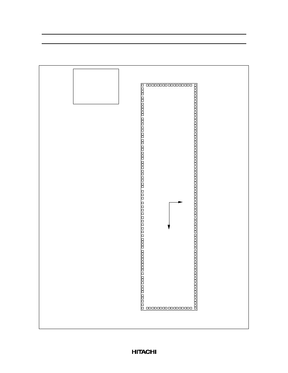
HD66727 Pad Coordinates
No.
Pad
Name
X
Y
No.
Pad
Name
X
Y
No.
Pad
Name
X
Y
No.
Pad
Name
X
Y
--
DUM1
≠5446
≠1244
46
KIN1
1737
≠1173
88
ASEG3
4212
1191
136
SEG39/22
≠1905
1196
1
V
CC
≠5146
≠1244
47
KIN2
1904
≠1173
89
ASEG4
4088
1191
137
SEG40/21
≠2029
1196
2
V
CC
≠5022
≠1244
48
KIN3
2071
≠1173
90
ASEG5
3963
1191
138
SEG41/20
≠2153
1196
3
V
CC
≠4898
≠1244
49
KST0
2261
≠1173
91
ASEG6
3839
1191
139
SEG42/19
≠2278
1196
--
DUM2
≠4648
≠1244
50
KST1
2421
≠1173
92
ASEG7
3714
1191
140
SEG43/18
≠2402
1196
--
DUM3
≠4524
≠1244
51
KST2
2581
≠1173
93
ASEG8
3590
1191
141
SEG44/17
≠2527
1196
4
V1OUT
≠4336
≠1169
52
KST3
2740
≠1173
94
ASEG9
3465
1191
142
SEG45/16
≠2651
1196
5
V2OUT
≠4216
≠1169
53
KST4
2900
≠1173
95
ASEG10
3341
1191
143
SEG46/15
≠2776
1196
6
V3OUT
≠4095
≠1169
54
KST5
3060
1173
96
ASEG11
3217
1191
144
SEG47/14
≠2900
1196
7
V4OUT
≠3975
≠1169
55
KST6
3220
≠1173
97
ASEG12
3092
1191
145
SEG48/13
≠3024
1196
8
V5OUT
≠3855
≠1169
56
KST7
3380
≠1173
98
SEG1/60
2824
1196
146
SEG49/12
≠3149
1196
9
VREFP
≠3734
≠1169
57
IRQ*
3539
≠1173
99
SEG2/59
2700
1196
147
SEG50/11
≠3273
1196
10
VREF
≠3614
≠1169
58
LED0
3716
≠1173
100
SEG3/58
2575
1196
148
SEG51/10
≠3398
1196
11
VREFM
≠3494
≠1169
59
LED1
3876
≠1173
101
SEG4/57
2451
1196
149
SEG52/9
≠3522
1196
12
V2
≠3373
≠1169
60
LED2
4036
≠1173
102
SEG5/56
2326
1196
150
SEG53/8
≠3647
1196
13
V3
≠3253
≠1169
61
PORT0
4228
≠1173
103
SEG6/55
2202
1196
151
SEG54/7
≠3771
1196
14
V
EE
≠3106
≠1168
62
PORT1
4403
≠1173
104
SEG7/54
2078
1196
152
SEG55/6
≠3896
1196
15
V
EE
2985
≠1168
63
PORT2
4578
≠1173
105
SEG8/53
1953
1196
153
SEG56/5
≠4020
1196
16
V5OUT3
≠2829
≠1168
64
GND
4735
≠1201
106
SEG9/52
1829
1196
154
SEG57/4
≠4144
1196
17
V5OUT3
≠2708
≠1168
65
GND
4855
≠1201
107
SEG10/51
1704
1196
155
SEG58/3
≠4269
1196
18
V5OUT2
≠2528
≠1168
66
GND
5054
≠1201
108
SEG11/50
1580
1196
156
SEG59/2
≠4393
1196
19
V5OUT2
≠2407
≠1168
67
AGND
5263
≠1201
109
SEG12/49
1455
1196
157
SEG60/1
≠4518
1196
20
C1
≠2216
≠1168
--
DUM4
5446
≠1201
110
SEG13/48
1331
1196
--
DUM10
≠4773
1260
21
C1
≠2095
≠1168
68
COM16/17
5446
≠1020
111
SEG14/47
1206
1196
--
DUM11
≠4898
1260
22
C1
≠1975
≠1168
69
COM15/18
5446
≠896
112
SEG15/46
1082
1196
--
DUM12
≠5022
1260
23
C2
≠1822
≠1168
70
COM14/19
5446
≠772
113
SEG16/45
958
1196
--
DUM13
≠5146
1260
24
C2
≠1701
≠1168
71
COM13/20
5446
≠647
114
SEG17/44
833
1196
--
DUM14
≠5446
1260
25
C2
≠1580
≠1168
72
COM12/21
5446
≠523
115
SEG18/43
709
1196
158
COM17/16
≠5446
970
26
VCI
≠1389
≠1168
73
COM11/22
5446
≠398
116
SEG19/42
584
1196
159
COM18/15
≠5446
845
27
VCI
≠1268
≠1168
74
COM10/23
5446
≠274
117
SEG20/41
460
1196
160
COM19/14
≠5446
721
28
GND
≠1083
≠1168
75
COM9/24
5446
≠149
118
SEG21/40
335
1196
161
COM20/13
≠5446
596
29
GND
≠962
≠1168
76
COM8/25
5446
≠25
119
SEG22/39
211
1196
162
COM21/12
≠5446
472
30
V
CC
≠792
≠1168
77
COM7/26
5446
100
120
SEG23/38
87
1196
163
COM22/11
≠5446
348
31
V
CC
≠672
≠1168
78
COM6/27
5446
224
121
SEG24/37
≠38
1196
164
COM23/10
≠5446
223
32
OSC2
≠459
≠1173
79
COM5/28
5446
348
122
SEG25/36
≠162
1196
165
COM24/9
≠5446
99
33
OSC1
≠315
≠1173
80
COM4/29
5446
473
123
SEG26/35
≠287
1196
166
COM25/8
≠5446
≠26
34
EXM
≠148
≠1173
81
COM3/30
5446
597
124
SEG27/34
≠411
1196
167
COM26/7
≠5446
≠150
35
OPOFF
19
≠1173
82
COM2/31
5446
722
125
SEG28/33
≠536
1196
168
COM27/6
≠5446
≠275
36
TEST
185
≠1173
83
COM1/32
5446
846
126
SEG29/32
≠660
1196
169
COM28/5
≠5446
≠399
37
RESET*
352
≠1173
84
COMS2/S1
5446
971
127
SEG30/31
≠785
1196
170
COM29/4
≠5446
≠524
38
IM
519
≠1173
--
DUM5
5446
1246
128
SEG31/30
≠909
1196
171
COM30/3
≠5446
≠648
39
VCCDUM1
666
≠1173
--
DUM6
5194
1246
129
SEG32/29
≠1033
1196
172
COM31/2
≠5446
≠772
40
ID0
789
≠1173
--
DUM7
5070
1246
130
SEG33/28
≠1158
1196
173
COM32/1
≠5446
≠897
41
VCCDUM2
937
≠1173
--
DUM8
4945
1246
131
SEG34/27
≠1282
1196
174
COMS1/S2
≠5446
≠1021
42
ID1
1059
≠1173
--
DUM9
4821
1246
132
SEG35/26
≠1407
1196
43
SCL
1226
≠1173
85
ACOM1
4585
1191
133
SEG36/25
≠1531
1196
44
SDA
1392
≠1173
86
ASEG1
4461
1191
134
SEG37/24
≠1656
1196
45
KIN0
1571
≠1173
87
ASEG2
4337
1191
135
SEG38/23
≠1780
1196
HD66727
8
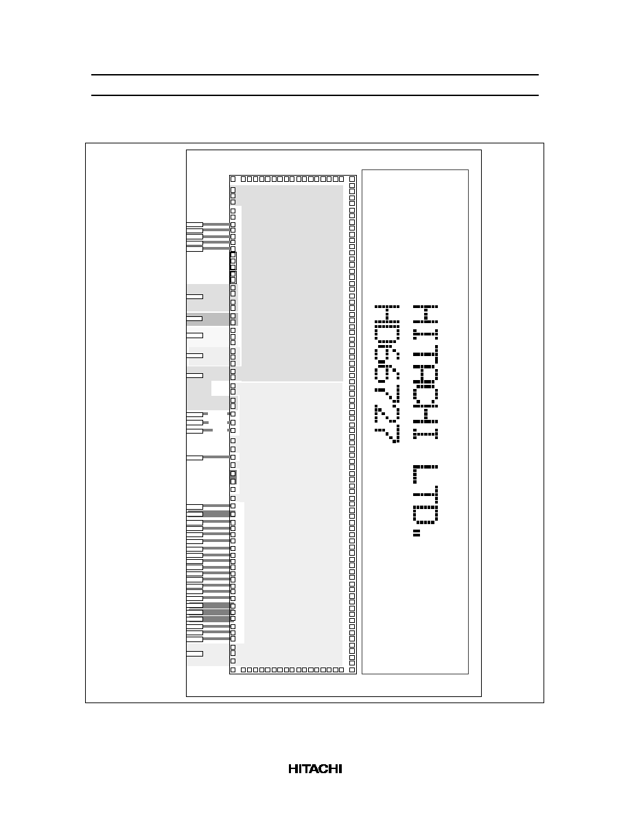
HD66727 Pad Arrangement
HD66727
SEG16/45
SEG15/46
SEG14/47
SEG13/48
SEG12/49
SEG11/50
SEG10/51
SEG9/52
SEG8/53
SEG7/54
SEG6/55
SEG5/56
SEG4/57
SEG3/58
SEG2/59
SEG26/35
SEG25/36
SEG24/37
SEG23/38
SEG22/39
SEG21/40
SEG20/41
SEG19/42
SEG18/43
SEG36/25
SEG35/26
SEG34/27
SEG33/28
SEG32/29
SEG31/30
SEG30/31
SEG29/32
SEG28/33
SEG27/34
SEG42/19
SEG41/20
SEG40/21
SEG39/22
SEG38/23
SEG37/24
SEG43/18
SEG17/44
SEG1/60
COM1/32
COMS2/S1
COM2/31
COM3/30
COM4/29
COM5/28
COM6/27
COM7/26
COM8/25
COM9/24
COM10/23
COM11/22
COM12/21
COM13/20
COM14/17
COM15/18
COM16/17
SEG44/17
SEG45/16
SEG46/15
SEG47/14
SEG48/13
SEG49/12
SEG50/11
SEG51/10
SEG52/9
SEG53/8
SEG54/7
SEG55/6
SEG56/5
SEG57/4
SEG58/3
SEG59/2
SEG60/1
COMS1/S2
COM32/1
COM31/2
COM30/3
COM29/4
COM28/5
COM27/6
COM25/8
COM24/9
COM23/10
COM22/11
COM21/12
COM20/13
COM19/14
COM18/15
COM17/16
ASEG10
ASEG9
ASEG8
ASEG7
ASEG6
ASEG5
ASEG4
ASEG3
ASEG2
ASEG1
ACOM1
OSC2
OSC1
RESET*
TEST
ID1/CS*
SDA
SCL
IRQ*
Vci
C2
C1
V5OUT2
V5OUT3
V3
V2
EXM
V
EE
COM26/7
GND
V
CC
V
CC
V
EE
Vci
AGND
OPOFF
C2
C1
V5OUT
V4OUT
V3OUT
V2OUT
V1OUT
V5OUT3
V5OUT2
GND
VREFP
VREF
VREFM
DUM10
DUM11
DUM12
DUM13
DUM9
DUM8
DUM7
DUM6
DUM4
GND
DUM1
Y
X
ID0
IM
KST0
KST1
KST2
KST3
KST4
KST5
KIN0
KIN1
KIN2
KIN3
VCCDUM1
ASEG11
ASEG12
KST6
KST7
GND
C2
C1
V
CC
V
CC
V
CC
PORT0
LED2
LED0
LED1
PORT1
PORT2
DUM2
DUM3
DUM5
DUM14
GND
VCCDUM2
(TOP view)
Chip size: 11.39
µ
m
◊
2.89
µ
m
Pad coordinates: Pad center
Coordinate origin: Chip center
Pad pitch:
Al pad size: 90
µ
m
◊
90
µ
m
Au bump size: 70
µ
m
◊
70
µ
m
120
µ
m
HD66727
9
Chip-on-Glass (COG) Mounting and Routing Examples
OSC2
TEST
ID1/CS*
Vci
C2
C1
V5OUT3
V3
V2
V
EE
GND
V
CC
V
CC
V
CC
V
EE
Vci
AGND
OPOFF
C2
C1
V5OUT
V4OUT
V3OUT
V2OUT
V1OUT
V5OUT3
V5OUT2
GND
VREFP
VREF
VREFM
Dummy
GND
V
CC
Dummy
ID0
IM
Vccdummy
Vccdummy
GND
C2
C1
V5OUT2
V
CC
OSC1
EXM
RESET*
SCL
SDA
IRQ*
KST0
KST1
KST2
KST3
KST4
KST5
KIN0
KIN1
KIN2
KIN3
KST6
KST7
PORT0
LED2
LED0
LED1
PORT1
PORT2
SCL
SDA
IRQ*
KST0
KST1
KST2
KST3
KST4
KST5
KIN0
KIN1
KIN2
KIN3
KST6
KST7
PORT0
LED2
LED0
LED1
PORT1
PORT2
GND
OSC2
OSC1
EXM
V
CC
C1
C2
V5OUT3
V5OUT2
Dummy
Dummy
IM="GND"
ID0="V
CC
"
ID1="GND"
OPOFF="GND"
TEST="V
CC
"
LCD Glass
HD66727
10
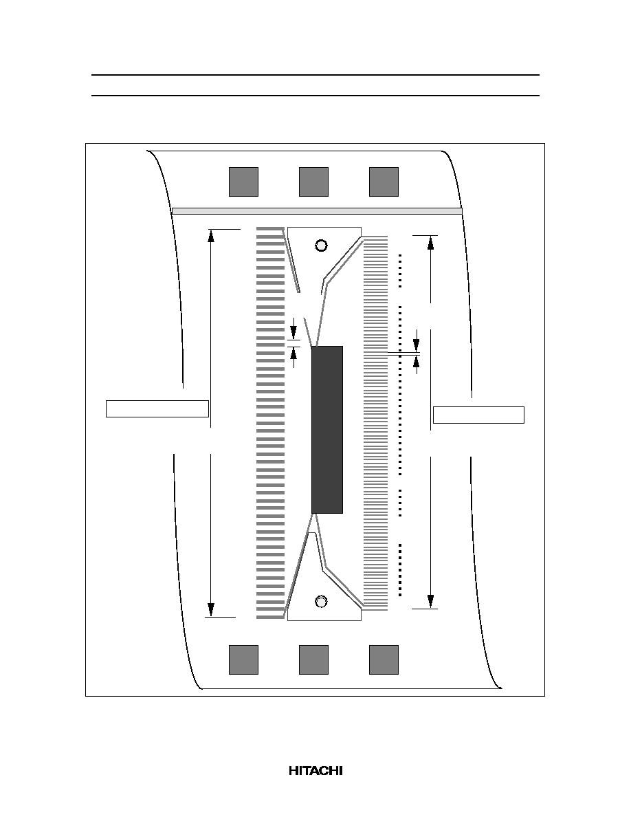
TCP Dimensions
COMS1/2
COM32/1
COM17/16
SEG60/1
SEG1/60
COM1/32
COM16/17
COMS2/1
Dummy
ASEG12
ASEG1
ACOMS
Dummy
0.60P
◊
(51-1)
= 30.0 mm
0.26P
◊
(109-1)
= 28.08 mm
0.26 mm
pitch
0.60mm
pitch
HIT
ACHI
HD66727
V
CC
V1OUT
V2OUT
V3OUT
V4OUT
V5OUT
V2
V3
V
EE
V5OUT3
V5OUT2
C1
C2
Vci
GND
V
CC
OSC2
OSC1
EXM
IM
OPOFF
TEST
RESET*
ID1/CS*
SCL
SDA
GND
AGND
VREFP
VREF
VREFM
ID0
IRQ*
KIN0
KIN1
KIN2
KIN3
KST1
KST2
KST3
KST4
KST5
KST0
KST6
KST7
LED0
LED1
LED2
PORT0
PORT1
PORT2
LCD driver outputs
I/O and power supply

HD66727
11
HD66727 Mounting Variations and Key-Matrix Configurations
R
C
C
COB board
LCD glass
LCD glass
R
C
C
Heat seal
Heat seal
LCD glass
Chip
R
C
C
TCP
Key-matrix board
Key-matrix board
Key-matrix board
(1) COB-1
(3) TCP
(2) COB-2
Chip
ON
F1
F2
1
2
3
4
5
6
7
8
9
0
#
ON
F1
F2
1
2
3
4
5
6
7
8
9
0
#
ON
F1
F2
1
2
3
4
5
6
7
8
9
0
#
LCD glass
Chip
R
C
C
Heat seal
Key-matrix board
(4) COG
ON
F1
F2
1
2
3
4
5
6
7
8
9
0
#
Chip
Figure 1 HD66727 Mounting Variations
Table 2
Configurations of LCD Modules (LCM) with Key Scan Function for Different Mounting
Methods
Parts
Chip-on-Board
(COB) Mounting 1
Chip-on-Board
(COB) Mounting 2
Tape-Carrier-
Package (TCP)
Mounting
Chip-on-Glass
(COG) Mounting
LCD glass
Necessary
Necessary
Necessary
Necessary
LCM (COB)
substrate
Necessary
Not necessary
Not necessary
Not necessary
HD66727
package
Bare chip
Bare chip
TCP
Bumped chip
Heat seal
Necessary
Necessary
Optional
Necessary
Key matrix
substrate
Necessary
Necessary
Necessary
Necessary

HD66727
12
Pin Functions
Table 3
Pin Functional Description
Signal
Number of
Pins
I/O
Connected to
Function
IM
1
I
V
CC
or GND
Selects the MPU interface mode:
Low: I
2
C bus mode
High: Clock-synchronized serial mode
ID1/ CS*
1
I
ID1: V
CC
or GND
CS*: MPU
Inputs the HD66727's identification code (ID1) in the I
2
C
bus mode.
Selects the HD66727 in the clock-synchronized serial
mode:
Low: HD66727 is selected and can be accessed
High: HD66727 is not selected and cannot be accessed
SDA
1
I/O
MPU
Inputs/outputs serial (receive/transmit) data and outputs
the acknowledge bit in the I
2
C bus mode.
Inputs/outputs serial (receive/transmit) data in the clock-
synchronized serial mode.
SCL
1
I
MPU
Inputs serial clock pulses. Serial data is latched at the
rising edge of each clock pulse.
ID0
1
I
V
CC
or GND
Inputs the HD66727's identification code in both
interface modes; must be fixed to high or low.
IRQ*
1
O
MPU
Generates the key scan interrupt signal.
KST0≠
KST7
8
O
Key matrix
Generates strobe signals for latching scanned data from
the key matrix at specific time interval.
KIN0≠KIN3 4
I
Key matrix
Samples key state from key matrix synchronously with
strobe signals.
LED0≠
LED2
3
O
LED back light
Output ports for control of LED or back light. Can draw 2
mA≠3 mA sink current. Also used as general ports.
PORT0≠
PORT2
3
O
General output
General output ports. These ports cannot drive current
such as LED control.
COMS1/2,
COMS2/1
2
O
LCD
Common output signals for segment-icon display.
COM1/32≠
COM32/1
32
O
LCD
Common output signals for character display: COM1 to
COM8 for the first line; COM9 to COM16 for the second
line, COM17 to COM24 for the third line, and COM25 to
COM32 for the fourth line. All the unused pins output
deselection waveforms. In the sleep mode (SLP = 1) or
standby mode (STB = 1), all pins output V
CC
level.
The CMS bit can change the shift direction of the
common signal. For example, if CMS = 0, COM1/32 is
COM1. If CMS = 1, COM1/32 is COM32.

HD66727
13
Table 3
Pin Functional Description (cont)
Signal
Number of
Pins
I/O
Connected to
Function
SEG1/60≠
SEG60/1
60
O
LCD
Segment output signals for segment-icon display and
character display. In the sleep mode (SLP = 1) or
standby mode (STB = 1), all pins output V
CC
level.
The SGS bit can change the shift direction of the
segment signal. For example, if SGS = 0, SEG1/60 is
SEG1. If SGS = 1, SEG1/60 is SEG60.
ACOM
1
O
LCD
Common output signal for annunciator display; can drive
display statically between V
CC
and AGND levels; outputs
V
CC
level while annunciator display is turned off (DA = 0).
ASEG1≠
ASEG12
12
O
LCD
Segment output signals for annunciator display; can
drive display statically between V
CC
and AGND levels;
output V
CC
level while annunciator display is turned off
(DA = 0).
V2, V3
2
I
Open or short-
circuited
V2 and V3 are voltage levels for the internal operational
amplifiers; can drive LCD with 1/4 bias when V2 and V3
are short-circuited and with 1/6 bias when they are left
disconnected.
VREFP,
VREF,
VREFM
3
I
Open or short-
circuited
Adjusts the driving capability of the internal operational
amplifiers according to the LCD power suppoly voltage.
LCD Power Supply
Pin Settings VREF,
Voltage (V
CC
≠V
EE
)
VREFP, and VREFM
V
CC
≠V
EE
: 3V≠5V
Only VREF and VREFP
shorted
V
CC
≠V
EE
: 4V≠6V
All pins open
V
CC
≠V
EE
: 5V≠8V
All pins shorted
V
CC
≠V
EE
: 7V or more
Only VREF and VREFM
shorted
V1OUT≠
V5OUT
5
I or O
Open or
external
bleeder-resistor
Used for output from the internal operational amplifiers
when they are used (OPOFF = GND); when amplifiers'
driving capability is insufficient, attach a capacitor to
stabilize the output. Especially these capacitors for
V1OUT and V4OUT must be attached in 1/26 duty and
1/34 duty. When the amplifiers are not used (OPOFF =
V
CC
), V1 to V5 voltages can be supplied to these pins
externally.
V
EE
2
--
Power supply
GND power supply for LCD drive. V
CC
≠ V
EE
13V.
V
CC
, GND
8
--
Power supply
V
CC
: +2.4V to +5.5V; GND (logic): 0V
AGND
1
--
Power supply
Low level power supply for annunciator display; can
adjust contrast of annunciators; AGND
GND.
OSC1,
OSC2
2
--
Oscillation-
resistor or clock
For R-C oscillation, connect an external resistor. For
external clock supply, input clock pulses to OSC1.

HD66727
14
Table 3
Pin Functional Description (cont)
Signal
Number of
Pins
I/O
Connected to
Function
Vci
2
I
Power supply
Inputs a reference voltage and supplies power to the
booster; generates the liquid crystal display drive
voltage from the operating voltage.
Vci = 1.0V to 5.0V
V
CC
V5OUT2
3
O
V
EE
pin/booster
capacitance
Voltage input to the Vci pin is boosted twice and output.
When the voltage is boosted three times, the same
capacitance as that of C1≠C2 should be connected
here.
V5OUT3
2
O
V
EE
pin
Voltage input to the Vci pin is boosted three times and
output.
C1, C2
6
--
Booster
capacitance
External capacitance should be connected here when
using the booster.
RESET*
1
I
MPU or external
R-C circuit
Reset pin. Initializes the LSI when low. Be sure to input
this signal after power-on.
EXM
1
I
MPU
External alternating signal used for annunciator display
in the standby mode. If annunciator display is not used,
EXM must be fixed to V
CC
or GND.
OPOFF
1
I
V
CC
or GND
Turns the internal operational amplifier off when OPOFF
= V
CC
, and turns it on when OPOFF = GND. If the
amplifier is turned off (OPOFF = V
CC
), V1 to V5 must be
supplied to the V1OUT to V5OUT pins.
V
CC
dummy 2
0
Input pad
Outputs V
CC
supply level; can fix the input pads to V
CC
level.
TEST
1
I
GND
Test pin. Must be fixed at GND level.

HD66727
15
Block Function Description
System Interface
The HD66727 has two types of system interfaces: I
2
C bus and clock-synchronized serial. The interface
mode is selected by the IM pin.
The HD66727 has two 8-bit registers: an instruction register (IR) and a data register (DR).
The IR stores instruction codes, such as clear display, return home, and display control, and address
information for display data RAM (DDRAM), character generator RAM (CGRAM), and segment RAM
(SEGRAM). The IR can only be written to by MPU and cannot be read from.
The DR temporarily stores data to be written into DDRAM, CGRAM, SEGRAM, or annunciator. Data
written into the DR from the MPU is automatically written into DDRAM, CGRAM, SEGRAM, or
annunciator by an internal operation. The DR is also used for data storage when reading data from
DDRAM, CGRAM, or SEGRAM. When address information is written into the IR, data is read and then
stored into the DR from DDRAM, CGRAM, or SEGRAM by an internal operation. Data transfer between
the MPU is then completed when the MPU reads the DR. After the read, data in DDRAM, CGRAM, or
SEGRAM at the next address is sent to the DR for the next read from the MPU.
These two registers and the operations can be selected by the register select bit (RS) and the read/write bit
(R/W) as listed in Table 4. For details, see the Serial Data Transfer section.
Table 4
Register Selection by RS and R/W Bits
RS Bit
R/W Bit
Operation
0
0
IR write as an internal operation
0
1
Read busy flag (DB7) and key scan data (DB3 to DB0)
1
0
DR write as an internal operation (DR to DDRAM, CGRAM, SEGRAM, or
annunciator)
1
1
DR read as an internal operation (DDRAM, CGRAM, or SEGRAM to DR)
Busy Flag (BF)
When the busy flag is 1, the HD66727 is in the internal operation mode, and the next instruction will not be
accepted. When RS = 0 and R/W = 1, the busy flag is output from DB7. The next instruction must be
written after ensuring that the busy flag is 0, or data must be transferred in appropriate timing considering
instruction execution times.

HD66727
16
Key Scan Registers (SCAN0 to SCAN7)
The key matrix scanner senses and holds the key states at each rising edge of the key strobe signals that are
output by the HD66727. The key strobe signals are output as time-multiplexed signals from KST0 to
KST7. After passing through the key matrix, these strobe signals are used to sample the key status on four
inputs KIN0 to KIN3, enabling up to 32 keys to be scanned.
The states of inputs KIN0 to KIN3 are sampled by key strobe signal KST0 and latched into register
SCAN0. Similarly, the data sampled by strobe signals KST1 to KST7 is latched into registers SCAN1 to
SCAN7, respectively.
Address Counter (AC)
The address counter (AC) assigns addresses to DDRAM, CGRAM, or SEGRAM. When the address set
instruction is written into the IR, the address information is sent from the IR to the AC. Selection of
DDRAM, CGRAM, and SEGRAM is also determined concurrently by the instruction. Figure 2 shows the
address counter and a sample DDRAM address setting to the address counter.
After writing into (reading from) DDRAM, CGRAM, or SEGRAM, the AC is automatically incremented
by 1 (or decremented by 1).
MSB
Example : DDRAM address 4A
Address
counter
(AC)
AC 6 AC5 AC4 AC3 AC2 AC1
LSB
AC0
1
0
0
1
0
1
0
Figure 2 Address Counter and Sample DDRAM Address Setting
Display Data RAM (DDRAM)
Display data RAM (DDRAM) stores display data represented in 8-bit character codes. Its capacity is 60
◊
8
bits, or 60 characters, which is equivalent to an area of 12 characters
◊
5 lines. Any number of display lines
(LCD drive duty ratio) from 1 to 4 can be selected by software. Here, assignment of DDRAM addresses is
the same for all display modes (Table 5). The line to be displayed at the top of the display (display-start
line) can also be selected by register settings. See Table 6.

HD66727
17
Table 5
DDRAM Addresses and Display Positions
Display
Line
1st
Char.
2nd
Char.
3rd
Char.
4th
Char.
5th
Char.
6th
Char.
7th
Char.
8th
Char.
9th
Char.
10th
Char.
11th
Char.
12th
Char.
1st
00
01
02
03
04
05
06
07
08
09
0A
0B
2nd
10
11
12
13
14
15
16
17
18
19
1A
1B
3rd
20
21
22
23
24
25
26
27
28
29
2A
2B
4th
30
31
32
33
34
35
36
37
38
39
3A
3B
5th
40
41
42
43
44
45
46
47
48
49
4A
4B
Note:
Char. indicates character position.
Table 6
Display-Line Modes, Display-Start Line, and DDRAM Addresses
Display-Start Lines
Display-
Line Mode
Duty
Ratio
Common
Pins
1st Line
(SN = 000)
2nd Line
(SN = 001)
3rd Line
(SN = 010)
4th Line
(SN = 011)
5th Line
(SN = 100)
1-line
(NL = 00)
1/10
COM1≠
COM8
"00"H≠"0B"H "10"H≠"1B"H "20"H≠"2B"H "30"H≠"3B"H "40"H≠"4B"H
2-line
(NL = 01)
1/18
COM1≠
COM8
"00"H≠"0B"H "10"H≠"1B"H "20"H≠"2B"H "30"H≠"3B"H "40"H≠"4B"H
COM9≠
COM16
"10"H≠"1B"H "20"H≠"2B"H "30"H≠"3B"H "40"H≠"4B"H "00"H≠"0B"H
3-line
(NL = 10)
1/26
COM1≠
COM8
"00"H≠"0B"H "10"H≠"1B"H "20"H≠"2B"H "30"H≠"3B"H "40"H≠"4B"H
COM9≠
COM16
"10"H≠"1B"H "20"H≠"2B"H "30"H≠"3B"H "40"H≠"4B"H "00"H≠"0B"H
COM17≠
COM24
"20"H≠"2B"H "30"H≠"3B"H "40"H≠"4B"H "00"H≠"0B"H "10"H≠"1B"H
4-line
(NL = 11)
1/34
COM1≠
COM8
"00"H≠"0B"H "10"H≠"1B"H "20"H≠"2B"H "30"H≠"3B"H "40"H≠"4B"H
COM9≠
COM16
"10"H≠"1B"H "20"H≠"2B"H "30"H≠"3B"H "40"H≠"4B"H "00"H≠"0B"H
COM17≠
COM24
"20"H≠"2B"H "30"H≠"3B"H "40"H≠"4B"H "00"H≠"0B"H "10"H≠"1B"H
COM25≠
COM32
"30"H≠"3B"H "40"H≠"4B"H "00"H≠"0B"H "10"H≠"1B"H "20"H≠"2B"H
Character Generator ROM (CGROM)
Character generator ROM (CGROM) generates 6
◊
8-dot character patterns from 8-bit character codes. It
can generate 240 6
◊
8-dot character patterns. Table 7 illustrates the relation between character codes and
character patterns for the Hitachi standard CGROM. User-defined character patterns are also available
using a mask-programmed ROM (see the Modifying Character Patterns section).

HD66727
18
Table 7
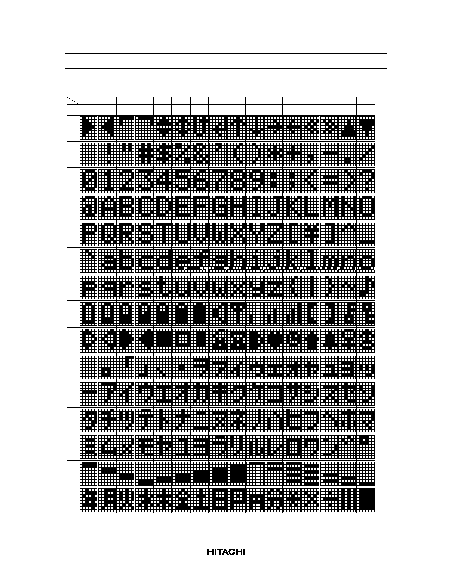
Relation between Character Codes and Character Patterns (ROM code: A03)
CGRAM
(1)
CGRAM
(4)
CGRAM
(3)
CGRAM
(2)
CGRAM
(1)
CGRAM
(4)
CGRAM
(3)
CGRAM
(2)
CGRAM
(1)
CGRAM
(4)
CGRAM
(3)
CGRAM
(2)
CGRAM
(1)
CGRAM
(4)
CGRAM
(3)
CGRAM
(2)
x 0
x F
x E
x D
x C
x B
x A
x 9
x 8
x 7
x 6
x 5
x 4
x 3
x 2
x 1
1 y
2 y
3 y
4 y
5 y
6 y
7 y
8 y
9 y
A y
B y
C y
D y
E y
F y
0 y
Lower
Upper
HD66727
19
Table 7
Relation between Character Codes and Character Patterns (ROM code: A04)
CGRAM
(1)
CGRAM
(4)
CGRAM
(3)
CGRAM
(2)
CGRAM
(1)
CGRAM
(4)
CGRAM
(3)
CGRAM
(2)
CGRAM
(1)
CGRAM
(4)
CGRAM
(3)
CGRAM
(2)
CGRAM
(1)
CGRAM
(4)
CGRAM
(3)
CGRAM
(2)
x 0
x F
x E
x D
x C
x B
x A
x 9
x 8
x 7
x 6
x 5
x 4
x 3
x 2
x 1
1 y
2 y
3 y
4 y
5 y
6 y
7 y
8 y
9 y
A y
B y
C y
D y
E y
F y
0 y
Lower
Upper
HD66727
20
Character Generator RAM (CGRAM)
Character generator RAM (CGRAM) of 32
◊
6 bits allows the user to redefine the character patterns. In the
case of 6
◊
8-dot characters, up to four characters may be redefined.
Write the character codes at addresses "00"H to "03"H into DDRAM to display the character patterns
stored in CGRAM (Table 8).
Table 8
Example of Relationships between Character Code (DDRAM) and Character Pattern
(CGRAM Data)
D7 D6 D5 D4 D3 D2 D1 D0
Character code (DDRAM data)
CGRAM data
LSB
MSB
A2 A1 A0
A4 A3
0
0
0
0
0
0
1
0
1
0
0
1
1
1
0
0
1
0
1
1
1
0
1
1
1
0
*
*
0
0
0
0
1
0
0
0
1
1
0
0
0
1
1
0
0
0
1
0
1
0
1
0
0
0
1
0
0
0
0
1
0
0
0
0
1
0
0
0
0
0
0
0
0
0
*
*
O4 O3 O2 O1 O0
O6
O7
CGRAM address
1
1
1
0
0
0
0
0
*
1
0
0
0
0
0
1
0
1
0
0
1
1
1
0
0
1
0
1
1
1
0
1
*
*
0
0
0
0
1
0
0
0
1
1
0
0
0
1
1
0
0
0
1
0
1
0
1
0
0
0
1
0
0
0
0
1
0
0
0
0
1
0
0
1
1
*
0
0
0
0
0
0
0
0
O5
0
0
0
0
0
0
0
0
Character
pattern
(1)
(Don't care)
(Don't care)
Character
pattern
(4)
Notes: 1. The lower 2 bits of the character code correspond to the upper two bits of the CGRAM address
(2 bits: 4 types).
2. CGRAM address bits 0 to 2 designate the character pattern raster-row position. The 8th raster-
row is the cursor position and its display is formed by a logical OR with the cursor.
3. In the 5-dot font width, the higher three bits of the CGRAM data are invalid; use the lower five
bits (O4 to O0). In the 6-dot font width, the higher two bits are invalid.
4. When the upper four bits (bits 7 to 4) of the character code are 0, CGRAM is selected.
Bits 3 and 2 of the character code are invalid (*). Therefore, for example, the character codes
00H and 08H correspond to the same CGRAM address.
5. A set bit in the CGRAM data corresponds to display selection, and 0 to non-selection.
Segment RAM (SEGRAM)
Segment RAM (SEGRAM) is used to enable control of segments such as icons and marks by the user
program. Segments and characters are driven by a multiplexing drive method.

HD66727
21
SEGRAM has a capacity of 8
◊
6 bits, for controlling the display of a maximum of 40 (48 in the 6-dot font
width) icons and marks. While COMS1 and COMS2 outputs are being selected, SEGRAM is read and
segments (icons and marks) are displayed by a multiplexing drive method (20 segments each during
COMS1 and COMS2 selection).
Bits in SEGRAM corresponding to segments to be displayed are directly set by the MPU, regardless of the
contents of DDRAM and CGRAM.
Tables 9 and 10 illustrate the correspondence between SEGRAM addresses and driver signals.
Table 9
Correspondence between Segment Display SEGRAM Addresses (ASEG) and Driver
Signals in the 5-Dot Font Width
ASEG Address
Segment Signals
Common
MSB
LSB D7
D6
D5
D4
D3
D2
D1
D0
Signal
1
0
0
0
*
*
*
SEG1,
SEG21,
SEG41
SEG2,
SEG22,
SEG42
SEG3,
SEG23,
SEG43
SEG4,
SEG24,
SEG44
SEG5,
SEG25,
SEG45
COMS1
1
0
0
1
*
*
*
SEG6,
SEG26,
SEG46
SEG7,
SEG27,
SEG47
SEG8,
SEG28,
SEG48
SEG9,
SEG29,
SEG49
SEG10,
SEG30,
SEG50
COMS1
1
0
1
0
*
*
*
SEG11,
SEG31,
SEG51
SEG12,
SEG32,
SEG52
SEG13,
SEG33,
SEG53
SEG14,
SEG34,
SEG54
SEG15,
SEG35,
SEG55
COMS1
1
0
1
1
*
*
*
SEG16,
SEG36,
SEG56
SEG17,
SEG37,
SEG57
SEG18,
SEG38,
SEG58
SEG19,
SEG39,
SEG59
SEG20,
SEG40,
SEG60
COMS1
1
1
0
0
*
*
*
SEG1,
SEG21,
SEG41
SEG2,
SEG22,
SEG42
SEG3,
SEG23,
SEG43
SEG4,
SEG24,
SEG44
SEG5,
SEG25,
SEG45
COMS2
1
1
0
1
*
*
*
SEG6,
SEG26,
SEG46
SEG7,
SEG27,
SEG47
SEG8,
SEG28,
SEG48
SEG9,
SEG29,
SEG49
SEG10,
SEG30,
SEG50
COMS2
1
1
1
0
*
*
*
SEG11,
SEG31,
SEG51
SEG12,
SEG32,
SEG52
SEG13,
SEG33,
SEG53
SEG14,
SEG34,
SEG54
SEG15,
SEG35,
SEG55
COMS2
1
1
1
1
*
*
*
SEG16,
SEG36,
SEG56
SEG17,
SEG37,
SEG57
SEG18,
SEG38,
SEG58
SEG19,
SEG39,
SEG59
SEG20,
SEG40,
SEG60
COMS2
Notes: 1. When the SFT pin is grounded, the SEG1 pin output is connected to the far left of the LCD
panel, and when the SFT pin is high, the SEG60 pin output is connected to the far left.
2. SEG1 to SEG20 data is identical to SEG21 to SEG40 and SEG41 to SEG60 data.
3. The lower five bits (D4 to D0) of SEGRAM data determine on or off display of each segment. A
segment is selected (turned on) when the corresponding data is 1, and is deselected (turned off)
when the corresponding data is 0. The upper three bits (D7 to D5) are invalid.

HD66727
22
Table 10
Correspondence between Segment Display SEGRAM Addresses (ASEG) and Driver
Signals in the 6-Dot Font Width
ASEG Address
Segment Signals
Common
MSB
LSB D7
D6
D5
D4
D3
D2
D1
D0
Signal
1
0
0
0
*
*
SEG1,
SEG25,
SEG49
SEG2,
SEG26,
SEG50
SEG3,
SEG27,
SEG51
SEG4,
SEG28,
SEG52
SEG5,
SEG29,
SEG53
SEG6,
SEG30,
SEG54
COMS1
1
0
0
1
*
*
SEG7,
SEG31,
SEG55
SEG8,
SEG32,
SEG56
SEG9,
SEG33,
SEG57
SEG10,
SEG34,
SEG58
SEG11,
SEG35,
SEG59
SEG12,
SEG36,
SEG60
COMS1
1
0
1
0
*
*
SEG13,
SEG37
SEG14,
SEG38
SEG15,
SEG39
SEG16,
SEG40
SEG17,
SEG41
SEG18,
SEG42
COMS1
1
0
1
1
*
*
SEG19,
SEG43
SEG20,
SEG44
SEG21,
SEG45
SEG22,
SEG46
SEG23,
SEG47
SEG24,
SEG48
COMS1
1
1
0
0
*
*
SEG1,
SEG25,
SEG49
SEG2,
SEG26,
SEG50
SEG3,
SEG27,
SEG51
SEG4,
SEG28,
SEG52
SEG5,
SEG29,
SEG53
SEG6,
SEG30,
SEG54
COMS2
1
1
0
1
*
*
SEG7,
SEG31,
SEG55
SEG8,
SEG32,
SEG56
SEG9,
SEG33,
SEG57
SEG10,
SEG34,
SEG58
SEG11,
SEG35,
SEG59
SEG12,
SEG36,
SEG60
COMS2
1
1
1
0
*
*
SEG13,
SEG37
SEG14,
SEG38
SEG15,
SEG39
SEG16,
SEG40
SEG17,
SEG41
SEG18,
SEG42
COMS2
1
1
1
1
*
*
SEG19,
SEG43
SEG20,
SEG44
SEG21,
SEG45
SEG22,
SEG46
SEG23,
SEG47
SEG24,
SEG48
COMS2
Notes: 1. When the SFT pin is grounded, the SEG1 pin output is connected to the far left of the LCD
panel, and when the SFT pin is high, the SEG60 pin output is connected to the far left.
2. SEG1 to SEG24 data are identical to SEG25 to SEG48 and SEG49 to SEG60 data.
3. The lower six bits (D5 to D0) of SEGRAM data determine on or off display for each segment. A
segment is selected (turned on) when the corresponding bit is 1, and is deselected (turned off)
when the corresponding bit is 0. The upper two bits (D7 to D6) are invalid.
Timing Generation Circuit
The timing generation circuit generates timing signals for the operation of internal circuits such as
DDRAM, CGROM, CGRAM, and SEGRAM. RAM read timing for display and internal operation timing
by MPU access are generated separately to avoid interfering with each other. Therefore, when writing data
to DDRAM, for example, there will be no undesirable interferences, such as flickering, in areas other than
the display area.
Cursor/Blink Control Circuit
The cursor/blink (or white-black inversion) control is used to produce a cursor or a flashing area on the
display at a position corresponding to the location stored in the address counter (AC).

HD66727
23
For example (Figure 3), when the address counter is 08H, a cursor is displayed at a position corresponding
to DDRAM address "08"H.
Cursor position
Display position
DDRAM address
Note: The cursor/blink or white-black inversion control is
also active when the address counter indicates the
CGRAM or SEGRAM. However, it has no effect on the
display.
1
2
3
4
5
6
7
8
11
9
10
12
00
01
02
03
04
05
06
07
0A
08
09
0B
Figure 3 Cursor Position and DDRAM Address
Multiplexing Liquid Crystal Display Driver Circuit
The multiplexing liquid crystal display driver circuit consists of 34 common signal drivers (COM1 to
COM32, COMS1, COMS2) and 60 segment signal drivers (SEG1 to SEG60). When the number of lines
are selected by a program, the required common signal drivers automatically output drive waveforms,
while the other common signal drivers continue to output deselection waveforms.
Character pattern data is sent serially through a 60-bit shift register and latched when all needed data has
arrived. The latched data then enables the segment signal drivers to generate drive waveform outputs.
The shift direction of 60-bit data can be changed by the SGS bit. The shift direction of the common driver
can also be changed by the CMS bit; select the direction appropriate for the device mounting configuration.
When multiplexing drive is not used, or during the standby or sleep mode, all the above common and
segment signal drivers output the V
CC
level, halting display.
Annunciator Driver Circuit
The static annunciator drivers, which are specially used for displaying icons and marks, consists of 1
common signal driver (ACOM) and 12 segment signal drivers (ASEG1 to ASEG12). Since this driver
circuit operates at the logic operating voltage (V
CC
to AGND), the LCD drive power supply circuit is not
necessary, and low-power consumption can be achieved. It is suitable for mark indication during system
standby because of its drive capability during the standby and sleep modes. When multiplexing drive is not
used, or during the standby or sleep mode, all the above common and segment signal drivers output the V
CC
level, halting display.
Tables 11 to 13 illustratate the correspondence between the annunciator addresses (AAN) and driver
signals.

HD66727
24
Table 11
Correspondence between Annunciator Display Addresses (AAN) and Driver Signals
AAN Address
Annunciator Segment Signals
Common
MSB
LSB D7
D6
D5
D4
D3
D2
D1
D0
Signal
0
0
0
0
ASEG1
ASEG2
ASEG3
ASEG4
ACOM
0
0
0
0
Blink
Data
Blink
Data
Blink
Data
Blink
Data
ACOM
0
0
0
1
ASEG5
ASEG6
ASEG7
ASEG8
ACOM
0
0
0
1
Blink
Data
Blink
Data
Blink
Data
Blink
Data
ACOM
0
0
1
0
ASEG9
ASEG10
ASEG11
ASEG12
ACOM
0
0
1
0
Blink
Data
Blink
Data
Blink
Data
Blink
Data
ACOM
Notes: 1. The annunciator is turned on when the corresponding even bit (data) is 1, and is turned off when
0.
2. The turned-on annunciator blinks when the corresponding odd bit (blink) is 1. Blinking is provided
by repeatedly turning on the annunciator for 32 frames and then turning it off for the next 32
frames.
Table 12
Correspondence between LED Driving Port Addresses (AAN) and Driver Signals
AAN Address
LED Driving and General Output Port
MSB
LSB D7
D6
D5
D4
D3
D2
D1
D0
0
0
1
1
*
*
Port2
Port1
Port0
LED2
LED1
LED0
General output port
LED driving port
Notes: 1. The LED bits are inverted and output from each LED pin. If 0 is set, the V
CC
level is output from
the LED pin. If 1 is set, the GND level is output from the LED pin.
2. The port bits output from each port pin. If 0 is set, the GND level is output from the PORT pin. If
1 is set, the V
CC
level is output from the PORT pin.
3. Current cannot be driven for outputs of the V
CC
level in LED2≠LED0 and the V
CC
and GND levels
in PORT2≠PORT0.
4. The upper two bits (D7 and D6) are invalid.
Table 13
Correspondence between SEG/COM Addresses (AAN) and Driver Signals
AAN Address
Shift Direction of SEG/COM Driver
MSB
LSB D7
D6
D5
D4
D3
D2
D1
D0
0
1
0
0
*
*
*
*
*
*
CMS
SGS
Notes: 1. If CMS = 0, COM1/32 is the first line of the first column, and COM32/1 is the 8th line of the fourth
column. If CMS = 1, COM1/32 is the 8th line of the fourth column, and COM32/1 is the first line
of the first column. If CMS = 0, COMS1/2 is COMS1, and COMS2/1 is COM2.
2. If SGS = 0, SEG1/60 is SEG1 in the left of the display, and SEG60/1 is SEG60 in the right of the
display. If SGS = 1, the shift direction of the SEG is reversed.
3. The upper six bits (D7≠D2) are invalid.

HD66727
25
LED Output Port
The HD66727 includes three LED/back-light driving output ports and three general output ports. These
ports can control the LED from the microcomputer through the serial interface.
Booster (DC-DC Converter)
The booster doubles or triples a voltage input to the Vci pin. With this function, both the internal logic units
and LCD drivers can be controlled with a single power supply.
Oscillator (OSC)
The HD66727 can provide R-C oscillation simply by adding an external oscillation-resistor between the
OSC1 and OSC2 pins. The appropriate oscillation frequency for operating voltage, display size, and frame
frequency can be obtained by adjusting the external-resistor value. Clock pulses can also be supplied
externally. Since R-C oscillation is halted during the standby mode, current consumption can be reduced.
V-Pin Voltage Followers
A voltage follower for each voltage level (V1 to V5) reduces current consumption by the LCD drive power
supply circuit. No external resistors are required because of the internal bleeder-resistor, which generates
different levels of LCD drive voltage. The voltage followers can be turned off while multiplexing drive is
not being used.
Contrast Adjuster
The contrast adjuster can adjust LCD contrast by varying LCD drive voltage by software. This function is
suitable for selecting appropriate brightness of the LCD or for temperature compensation.
HD66727
26
Modifying Character Patterns
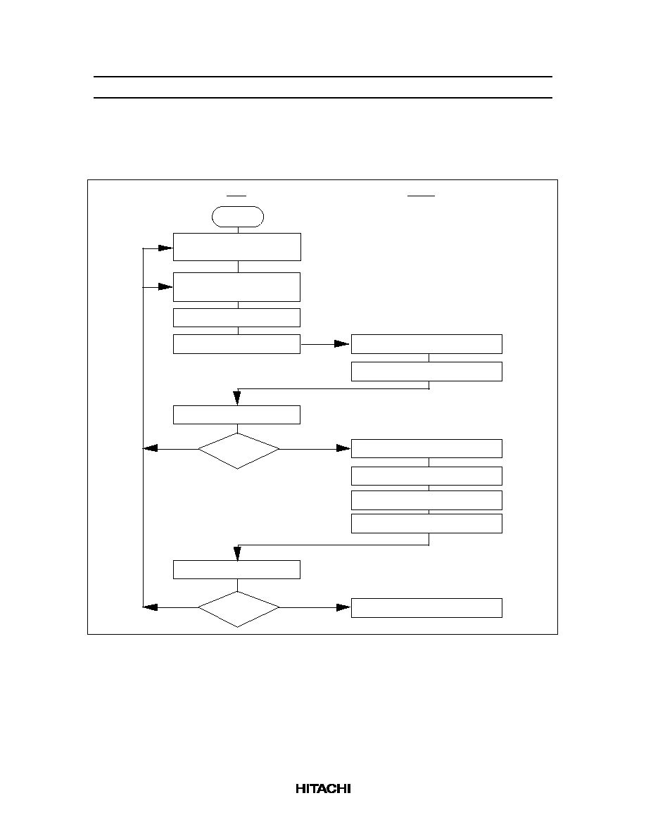
Character pattern development procedure
Start
Write EPROM
Art work
OK ?
masking
Trial
Sample
OK ?
Sample evaluation
Hitachi
User
No
No
Yes
Yes
EPROM Hitachi
Determine character
patterns
Create EPROM
address data listing
Computer processing
Create character pattern listing
Mass production
Evaluate character patterns
Figure 4 Character Pattern Development Procedure

HD66727
27
The following operations correspond to the numbers listed in Figure 4:
1. Determine the correspondence between character codes and character patterns.
2. Create a listing indicating the correspondence between EPROM addresses and data.
3. Program the character patterns into an EPROM.
4. Send the EPROM to Hitachi.
5. Computer processing of the EPROM is performed at Hitachi to create a character pattern listing, which
is sent to the user.
6. If there are no problems within the character pattern listing, a trial LSI is created at Hitachi and samples
are sent to the user for evaluation. When it is confirmed by the user that the character patterns are
correctly written, mass production of the LSI will proceed at Hitachi.
HD66727
28
Programming Character Patterns
This section explains the correspondence between addresses and data used to program character patterns in
EPROM.
Programming to EPROM: The HD66727 character generator ROM can generate 240 6
◊
8-dot character
patterns. Table 14 shows correspondence between the EPROM address, data, and the character pattern.
Table 14
Example of Correspondence between EPROM Address, Data, and Character Pattern
(6
◊
8 Dots)
A10 A9 A8 A7 A6 A5 A4 A3
A2 A1 A0
0
0
0
0
0
1
0
1
0
0
1
1
1
0
0
1
0
1
1
1
0
1
1
1
1
0
0
0
1
O4 O3 O2 O1 O0
1
0
0
0
1
1
0
0
0
1
0
1
0
1
0
0
0
1
0
0
0
0
1
0
0
0
0
1
0
0
0
0
0
0
0
0
O5
0
0
0
0
0
0
0
Character code
Line position
EPROM Address
Data
LSB
MSB
0
0
0
0
0
0
0
0
0
A11
0
1
0
1
1
0
0
1
Notes: 1. EPROM address bits A11 to A4 correspond to a character code.
2. EPROM address bits A2 to A0 specify the line position of the character pattern. EPROM address
bit A3 must be set to 0.
3. EPROM data bits O5 to O0 correspond to character pattern data.
4. Areas which are lit (indicated by shading) are stored as 1, and unlit areas as 0.
5. The eighth raster-row is also stored in the CGROM, and must also be programmed. If the eighth
raster-row is used for a cursor, this data must all be set to zero.
6. EPROM data bits O7 to O6 are invalid. 0 must be written in all bits.
Handling Unused Character Patterns:
1. EPROM data outside the character pattern area: This is ignored by character generator ROM for display
operation so any data is acceptable.
2. EPROM data in CGRAM area: Always fill with zeros.
3. Treatment of unused user patterns in the HD66727 EPROM: According to the user application, these
are handled in either of two ways:
a. When unused character patterns are not programmed: If an unused character code is written into
DDRAM, all its dots are lit, because the EPROM is filled with 1s after it is erased.
b. When unused character patterns are programmed as 0s: Nothing is displayed even if unused
character codes are written into DDRAM. (This is equivalent to a space.)

HD66727
29
Instructions
Outline
Only the instruction register (IR) and the data register (DR) of the HD66727 can be controlled by the MPU.
Before starting internal operation of the HD66727, control information is temporarily stored in these
registers to allow interfacing with various peripheral control devices or MPUs which operate at different
speeds. The internal operation of the HD66727 is determined by signals sent from the MPU. These signals,
which include register selection bit (RS), read/write bit (R/W), and the data bus (DB0 to DB7), make up the
HD66727 instructions. There are four categories of instructions that:
∑
Control display
∑
Control key scan
∑
Control power management
∑
Set internal RAM addresses
∑
Perform data transfer with internal RAM
Normally, instructions that perform data transfer with internal RAM are used the most. However, auto-
incrementation by 1 (or auto-decrementation by 1) of internal HD66727 RAM addresses after each data
write can lighten the program load of the MPU.
While an instruction is being executed for internal operation, or during reset, no instruction other than the
busy flag/key scan read instruction can be executed.
Because the busy flag is set to 1 while an instruction is being executed, check it to make sure it is 0 before
sending another instruction from the MPU. If an instruction is sent without checking the busy flag, the time
between the first instruction issue and next instruction issue must be longer than the instruction execution
time itself. Refer to Table 23 for the list of each instruction execution cycles (clock pulses). The execution
time depends on the operating clock frequency (oscillation frequency).
HD66727
30
Instruction Description
Busy Flag/Key Scan Read
The busy flag/key scan read instruction (Figure 5) reads scan data SD3 to SD0 latched into scan registers
SCAN0 to SCAN7, scan cycle state SF1 and SF0, and transfer flag TF, sequentially. It also reads the busy
flag (BF) indicating that the system is now internally operating on a previously received instruction. If BF
is 1, the internal operation is in progress. The next instruction will not be accepted until BF is cleared to 0.
Adjust the data transfer rate so that the last bit of the next instruction is received after BF is cleared to 0.
0
DB7
DB0
1
BF
SF1 SF0
TF SD3 SD2 SD1 SD0
RS R/W
Figure 5 Busy Flag/Key Scan Read Instruction
Clear Display
The clear display instruction (Figure 6) writes space code 20H (character pattern for character code 20H
must be a blank pattern) into all DDRAM addresses. It then sets DDRAM address 0 into the address
counter. It also sets I/D to 1 (increment mode) in the entry mode set instruction.
0
0
0
0
0
0
0
0
0
1
RS R/W DB7
DB0
Figure 6 Clear Display Instruction
Return Home
The return home instruction (Figure 7) sets DDRAM address 0 into the address counter. The DDRAM
contents do not change. The cursor or blinking goes to the top left of the display.
0
0
0
0
0
0
0
0
1
0
RS R/W DB7
DB0
Figure 7 Return Home Instruction

HD66727
31
Start Oscillator
The start oscillator instruction (Figure 8) re-starts the oscillator from a halt state in the standby mode. After
issuing this instruction, wait at least 10 ms for oscillation to become stable before issuing the next
instruction. (Refer to the Standby Mode section.)
0
0
0
0
0
0
0
0
1
1
RS R/W DB7
DB0
Figure 8 Start Oscillator Instruction
Entry Mode Set
The entry mode set instruction (Figure 9) includes the I/D and OSC bits.
I/D: Increments (I/D = 1) or decrements (I/D = 0) the DDRAM address by 1 when a character code is
written into or read from DDRAM. The cursor or blinking moves to the right when incremented by 1 and
to the left when decremented by 1. The same applies to writing and reading of CGRAM and SEGRAM.
OSC: Divides the external clock frequency by four (OSC = 1) and uses the resulting clock as an operating
clock for all internal operations. The execution time for this instruction and subsequent ones is therefore
quadrupled. The execution time of clearing this bit (OSC = 0) is also quadrupled. Note that, the key scan
cycle is affected. For details, refer to the Partial-Display-Off Function section.
0
0
0
0
0
0
0
1
I/D
OSC
RS R/W DB7
DB0
Figure 9 Entry Mode Set Instruction
Cursor Control
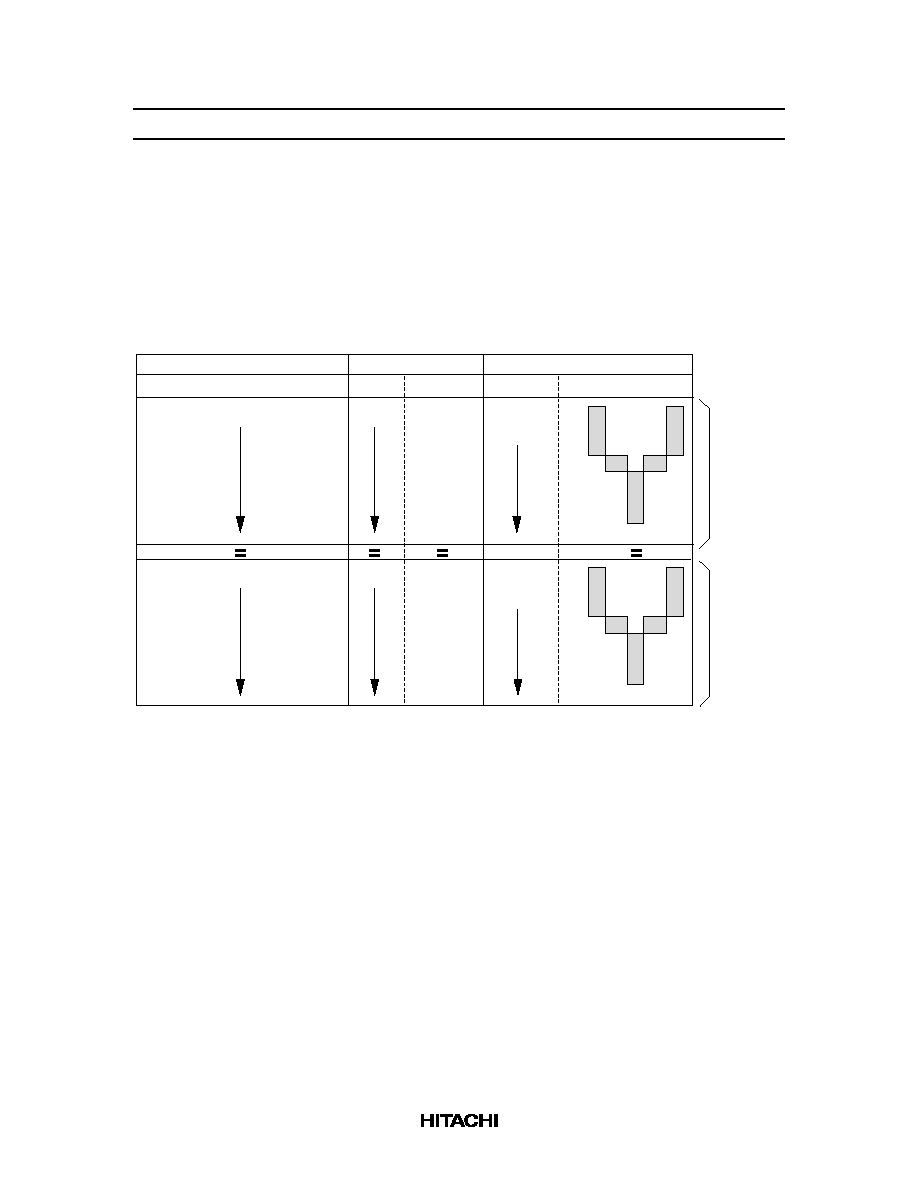
The cursor control instruction (Figure 10) includes the B/W, C, and B bits.
B/W: When B/W is 1, the character at the cursor position is cyclically (every 32 frames) displayed with
black-white inversion.
C: The cursor is displayed on the 8th raster-row when C is 1. The cursor is displayed using 5 dots in the 8th
raster-row for 5
◊
8-dot character font, or 6 dots in the 8th raster-row for 6
◊
8 dot character font.
B: The character indicated by the cursor blinks when B is 1. The blinking is displayed as switching
between all black dots and displayed characters every 32 frames. The cursor and blinking can be set to
display simultaneously. When LC and B = 1, the blinking is displayed as switching between all white dots
and displayed characters.
Figure 11 shows cursor control examples.
HD66727
32
0
0
0
0
0
0
1 B/W
C
B
RS R/W DB7
DB0
Figure 10 Cursor Control Instruction
Alternating display
(every 32 frames)
Alternating
display
i) White-black inverting display example
ii) 8th raster-row
cursor display
ii) Blink display example
Figure 11 Cursor Control Examples
Display On/Off Control
The display on/off control instruction (Figure 12) includes the D, FW, and LC bits.
D: The character display and the segment display for multiplexing icon are on when D is 1. When off, the
display data remains in DDRAM or SEGRAM, and can be displayed instantly by setting D to 1. When D is
0, multiplexing LCD drive halts and the display is off with the SEG1 to SEG60 outputs, COM1 to COM32
outputs, and COMS1/2 output set to V
CC
level and off. Because of this, the HD66727 can control charging
current for the LCD with driving.
FW: When FW = 0, the font width is 5 dots. When FW = 1, the font width is 6 dots.
LC: When LC = 1, a cursor attribute is assigned to the line that contains the address counter (AC) value.
Cursor mode can be selected with the B/W, C, and B bits. Refer to the Line-Cursor Display section.
0
0
0
0
0
1
0
D
FW
LC
RS R/W DB7
DB0
Figure 12 Display On/Off Control Instruction

HD66727
33
Power Control
The power control instruction (Figure 13) includes the AMP, SLP, and STB bits.
AMP: When AMP = 1, each voltage follower for V1 to V5 pins and the booster are turned on. When AMP
= 0, current consumption can be reduced while character or segment display controlled by the multiplexing
drive method is not being used.
SLP: When SLP = 1, the HD66727 enters the sleep mode, where all the internal operations are halted
except for the annunciator display function, key scan function, and the R-C oscillator, thus reducing current
consumption. For details, refer to the Sleep Mode section. Only the following instructions can be executed
during the sleep mode.
1. Annunciator address (AAN) set
2. Annunciator data write
3. LED drive/general output port data write
4. Annunciator display on or off (DA = 1 or 0)
5. Voltage follower on or off (AMP = 1 or 0)
6. Standby mode set (STB = 1)
7. Sleep mode cancel (SLP = 0)
8. Key scan data (SD) read
9. Key scan interrupt generation enable/disable (IRE = 1 or 0)
10. Key scan cycle (KF) set
During the sleep mode, the other RAM data and instructions cannot be updated but they are retained.
STB: When STB = 1, the HD66727 enters the standby mode, where the device completely stops, halting all
the internal operations including the internal R-C oscillator and no external clock pulses are supplied.
However, annunciator display alone is available when the alternating signal for annunciator-driving signals
is supplied to the EXM pin. When the annunciator display is not needed, make sure to turn off display (DA
= 0). Normal key scanning is also halted in the standby mode. However, the HD66727 can detect four key
inputs connected with strobe signal KST0, thus generating the key scan interrupt (IRQ*). For details, refer
to the Standby Mode section and the Key Scan Interrupt section. Only the following instructions can be
executed during the standby mode.
1. Annunciator address (AAN) set
2. Annunciator data write
3. LED drive/general output port data write
4. Annunciator display on or off (DA = 1 or 0)
5. Voltage follower on or off (AMP = 1 or 0)
6. Start oscillator
7. Standby mode cancel (STB = 0)
8. Key scan interrupt generation enable/disable (IRE = 1 or 0)
HD66727
34
During the standby mode, the other RAM data and instructions may be lost; they must be set again after the
standby mode is canceled.
0
0
0
0
0
1
1 AMP SLP
STB
RS R/W DB7
DB0
Figure 13 Power Control Instruction
Display Control
The display control instruction (Figure 14) includes the NL and DL bits.
NL1, NL0: Designates the number of display lines. This value determines the LCD drive multiplexing duty
ratio (Table 15). The address assignment is the same for all display line modes.
DL3≠DL1: Doubles the height of characters on a specified line. The first, second, or third line is doubled in
height when DL1, DL2, or DL3 = 1, respectively. Two lines can be simultaneously doubled in a 4-line
display. Refer to the Double-Height Display section.
0
RS R/W DB7
DB0
0
0
0
1
NL1 NL0 DL3 DL2 DL1
Figure 14 Display Control Instruction
Table 15
NL Bits and Display Lines
NL1
NL0
Number of Display Lines
LCD Drive Multiplexing Duty Ratio
0
0
1
1/10
0
1
2
1/18
1
0
3
1/26
1
1
4
1/34
Contrast Control
The contrast control instruction (Figure 15) includes the SN and CT bits.
SN2: Combined with the SN1 and SN0 bits described in the Scroll Control section to select the top line to
be scrolled (display-start line).
CT3≠CT0: Controls the LCD drive voltage (potential difference between V
CC
and V5) to adjust contrast
(Figure 16 and Table 16). For details, refer to the Contrast Adjuster section.

HD66727
35
0
0
0
1
0
SN2 CT3 CT2 CT1 CT0
RS R/W DB7
DB0
Figure 15 Contrast Control Instruction
V
CC
V2
V3
R
R
R
R
R
VR
≠
+
≠
+
≠
+
≠
+
R
≠
+
V
EE
HD66727
Figure 16 Contrast Adjuster
Table 16
CT Bits and Variable Resistor Value of Contrast Adjuster
CT3
CT2
CT1
CT0
Variable Resistor Value (VR)
0
0
0
0
6.4 x R
0
0
0
1
6.0 x R
0
0
1
0
5.6 x R
0
0
1
1
5.2 x R
0
1
0
0
4.8 x R
0
1
0
1
4.4 x R
0
1
1
0
4.0 x R
0
1
1
1
3.6 x R
1
0
0
0
3.2 x R
1
0
0
1
2.8 x R
1
0
1
0
2.4 x R
1
0
1
1
2.0 x R
1
1
0
0
1.6 x R
1
1
0
1
1.2 x R
1
1
1
0
0.8 x R
1
1
1
1
0.4 x R

HD66727
36
Scroll Control
The scroll control instruction (Figure 17) includes the SN and SL bits.
SN1, SN0: Combined with the SN2 bit described in the Contrast Control section to select the top line to be
displayed (display-start line) through the data output from the COM1 pin (Table 17). After first five lines
are displayed from the top line, the cycle is repeated and scrolling continues.
SL2≠SL0: Selects the top raster-row to be displayed (display-start raster-row) in the display-start line
specified by SN2 to SN0. Any raster-row from the first to eighth can be selected (Table 18). This function
is used to perform vertical smooth scroll together with SN2 to SN0. For details, refer to the Vertical
Smooth Scroll section.
0
0
0
1
1
SN1 SN0 SL2 SL1 SL0
RS R/W DB7
DB0
Figure 17 Scroll Control Instruction
Table 17
SN Bits and Display-Start Lines
SN2
SN1
SN0
Display-Start Line
0
0
0
1st line
0
0
1
2nd line
0
1
0
3rd line
0
1
1
4th line
1
0/1
0/1
5th line
Table 18
SN Bits and Display-Start Raster-Rows
SL2
SL1
SL0
Display-Start Raster-Row
0
0
0
1st raster-row
0
0
1
2nd raster-row
0
1
0
3rd raster-row
0
1
1
4th raster-row
1
0
0
5th raster-row
1
0
1
6th raster-row
1
1
0
7th raster-row
1
1
1
8th raster-row

HD66727
37
Annunciator/SEGRAM Address Set
The annunciator/SEGRAM address set instruction (Figure 18) includes the DA and A (AAN/ASEG) bits.
DA: Turns annunciator display on or off. When DA = 1, annunciator display is turned on and driven
statically. When DA = 0, annunciator display is turned off with ASEG1 to ASEG10 and ACOM pins held
to V
CC
level.
The internal operating clock supply is halted during the standby mode; make sure to turn off display (DA =
0) if the external alternating signal is not supplied. For details, refer to the Segment Display and
Annunciator Display section and the Standby Mode section.
AAAA: Used for setting the SEGRAM address into the address counter (AC) or for directly setting the
annunciator address. The SEGRAM addresses range from 1000H to 1111H (8 addresses), while the
annunciator addresses range from 0000H to 0010H (3 addresses).
The annunciator address is directly set without using the address counter, and consequently must be
updated for each access. The annunciator address can be set even during the sleep and standby modes.
Once the SEGRAM address is set, data in the SEGRAM can be accessed consecutively since the address
counter is automatically incremented or decremented by one according to the I/D bit setting after each
access. The SEGRAM address cannot be set during the sleep or standby mode.
AAAA is the address for setting the 0011 LED/general port data; 0100 is the address for setting the
SEG/COM shift direction. See 'Annunciator Driver Circuit' for details.
0
RS R/W DB7
DB0
0
1
0
0
DA
A
A
A
A
Figure 18 Annunciator/SEGRAM Address Set Instruction

HD66727
38
Table 19
Annunciator/LED/SEG/COM Shift Direction/SEGRAM Address Set
Address
A
A
A
A
DB7
DB6
DB5
DB4
DB3
DB2
DB1
DB0
Annunciator
0
0
0
0
ASEG1
ASEG2
ASEG3
ASEG4
address
0
0
0
1
ASEG5
ASEG6
ASEG7
ASEG8
0
0
1
0
ASEG9
ASEG10
ASEG11
ASEG12
LED port address
0
0
1
1
*
*
PORT2 PORT1 PORT0 LED2
LED1
LED0
SEG/COM shift
direction address
0
1
0
0
*
*
*
*
*
*
CMS
SGS
SEGRAM
1
0
0
0
*
*
SEGRAM data in COMS1 side
address
1
0
0
1
*
*
1
0
1
0
*
*
1
0
1
1
*
*
1
1
0
0
*
*
SEGRAM data in COMS2 side
1
1
0
1
*
*
1
1
1
0
*
*
1
1
1
1
*
*
CGRAM Address Set
The CGRAM address set instruction (Figure 19) includes the A (ACG) bits.
AAAAA: Used for setting the CGRAM address into the address counter (AC). The CGRAM addresses
range from 00H to 1FH (32 addresses) (Table 19).
Once the CGRAM address is set, data in the CGRAM can be accessed consecutively since the address
counter is automatically incremented or decremented according to the I/D bit setting after each access. The
CGRAM address cannot be set during the sleep or standby mode.
0
RS R/W DB7
DB0
0
1
0
1
A
A
A
A
A
Figure 19 CGRAM Address Set Instruction

HD66727
39
Table 20
CGRAM Addresses and Character Codes
Displayed Character
CGRAM Address
Character Codes
1st character
"00"H to "07"H
"00"H
2nd character
"08"H to "0F"H
"01"H
3rd character
"10"H to "17"H
"02"H
4th character
"18"H to "1F"H
"03"H
DDRAM Address Set
The DDRAM address set instruction (Figure 20) includes the A (ADD), IRE, and KF bits.
AAAAAAA: Used for setting the DDRAM address into the address counter (AC). The DDRAM addresses
range from "00"H to "4B"H (60 addresses) (Table 21).
Once the DDRAM address is set, data in the DDRAM can be accessed consecutively since the address
counter is automatically incremented or decremented according to the I/D bit setting after each access.
Here, invalid addresses are automatically skipped. The DDRAM address cannot be set during the sleep or
standby mode.
0
RS R/W DB7
DB0
Upper bits
Lower bits
0
1
1
0
IRE KF1 KF0
A
A
0
0
1
1
1
A
A
A
A
A
Figure 20 DDRAM Address Set Instruction
Table 21
DDRAM Addresses and Invalid Addresses
Displayed Line
DDRAM Address
Invalid Addresses
1st line
"00"H to "0B"H
"0C"H to "0F"H
2nd line
"10"H to "1B"H
"1C"H to "1F"H
3rd line
"20"H to "2B"H
"2C"H to "2F"H
4th line
"30"H to "3B"H
"3C"H to "3F"H
5th line
"40"H to "4B"H
"4C"H and subsequent addresses

HD66727
40
IRE: When IRE is 1, the key scan interrupt (IRQ*) generation is enabled. When a key is pressed, the IRQ*
pin outputs a low level signal.
KF1, KF0: Used for specifying the key scan cycle. Set these bits according to the mechanical
characteristics of the keys and the oscillation frequency (Table 22).
Table 22
KF Bits and Key Scan Cycles
NL1
KF1
KF0
Key Scan Cycle
Key Strobe Width
1 or 2 display lines (NL1=0)
0
0
160/fosc
20/fosc
1 or 2 display lines (NL1=0)
0
1
320/fosc
40/fosc
1 or 2 display lines (NL1=0)
1
0
640/fosc
80/fosc
1 or 2 display lines (NL1=0)
1
1
1,280/fosc
160/fosc
3 or 4 display lines (NL1=1)
0
0
320/fosc
40/fosc
3 or 4 display lines (NL1=1)
0
1
640/fosc
80/fosc
3 or 4 display lines (NL1=1)
1
0
1,280/fosc
160/fosc
3 or 4 display lines (NL1=1)
1
1
2,560/fosc
320/fosc
Note:
fosc is the oscillation frequency or external clock frequency.
HD66727
41
Write Data to RAM
The write data to RAM instruction (Figure 21) writes 8-bit data to annunciator or DDRAM, lower 6-bit
data to LED port, SEGRAM or CGRAM, or lower two bits to shift direction change bits of SEG/COM that
is selected by the previous specification of the address set instruction (annunciator/LED/SEGRAM address
set, CGRAM address set, or DDRAM address set).
After a write, the address is automatically incremented or decremented by 1 according to the I/D bit setting
in the entry mode set instruction. The annunciator or LED port address is not automatically updated; it must
be specifically updated to write data to a different address. During the sleep and standby modes, DDRAM,
CGRAM, or SEGRAM cannot be accessed.
1
RS R/W DB7
DB0
0
D
D
D
D
D
D
D
D
Figure 21 Write Data to RAM Instruction
Read Data from RAM
The read data from RAM instruction (Figure 22), reads 8-bit data from DDRAM, or 5-bit data from
CGRAM or SEGRAM that is selected by the previous specification of the address set instruction
(SEGRAM address set, CGRAM address set, or DDRAM address set). The unused upper three bits of
CGRAM or SEGRAM data are read as 000; annunciator data cannot be read. If no address is specified by
the address set instruction just before this instruction, the first data read will be invalid. When executing
consecutive read instructions, the next data is normally read from the next address.
After a read, the address is automatically incremented or decremented by 1 according to the I/D bit setting
in the entry mode set instruction.
1
RS R/W DB7
DB0
1
D
D
D
D
D
D
D
D
Figure 22 Read Data from RAM Instruction

HD66727
42
Table 23
Instruction List
Code
Execution
No.
Instruction
R/W RS
DB7 DB6 DB5 DB4 DB3 DB2 DB1 DB0 Description
Cycle
*1
KS
Busy
flag/key scan
read
1
0
BF
SF
TF
SD
Reads busy flag (BF), key-
scan state (SF and TF),
and data in key scan
registers (SD).
0
CL
Clear display 0
0
0
0
0
0
0
0
0
1
Clears entire display and
sets address 0 into the
address counter.
310
CH
Return home 0
0
0
0
0
0
0
0
1
0
Sets DDRAM address 0
into the address counter.
5
OS
Start
oscillator
0
0
0
0
0
0
0
0
1
1
Starts the oscillation
standby mode.
--
EM
Entry mode
set
0
0
0
0
0
0
0
1
I/D
OSC Sets the address update
direction after RAM access
(I/D), and system clock
division (OSC).
5
CR
Cursor
control
0
0
0
0
0
0
1
B/W C
B
Sets black-white inverting
cursor (B/W), 8th raster-
row cursor (C), and blink
cursor (B).
5
DO
Display
on/off control
0
0
0
0
0
1
0
D
FW
LC
Sets character/segment
display on (D), font width
(FW), and line-cursor
display (LC).
5
PW
Power
control
0
0
0
0
0
1
1
AMP SLP STB Turns on LCD power
supply (AMP), and sets
the sleep mode (SLP) and
standby mode (STB).
5
DC
Display
control
0
0
0
0
1
NL1 NL0 DL3 DL2 DL1 Sets the number of display
lines (NL) and the lines to
be doubled in height.
5
CN
Contrast
control
0
0
0
1
0
SN2
CT
Sets the display-start line
(SN2) and contrast-
adjusting value (CT).
5
SC
Scroll control 0
0
0
1
1
SN1 SN0
SL
Sets the display-start line
(SN) and display-start
raster-row (SL).
5
AS
Annunciator/
SEGRAM
address set
0
0
1
0
0
DA
AAN/ASEG
Turns on the annunciator
display (DA) and sets
annunciator/SEGRAM
address.
5
CA
CGRAM
address set
0
0
1
0
1
ACG
Sets the initial CGRAM
address to the address
counter.
5

HD66727
43
Table 23
Instruction List (cont)
Code
Execution
No.
Instruction
R/W RS
DB7 DB6 DB5 DB4 DB3 DB2 DB1 DB0 Description
Cycle
*1
DA
DDRAM
address set
(upper bits)
0
0
1
1
0
IRE
KF1 KF0
ADD
(upper
bits)
Sets the initial higher
DDRAM address to the
address counter, and key
scan cycle.
5
DA
DDRAM
address set
(lower bits)
0
0
1
1
1
ADD (lower bits)
Sets the initial lower
DDRAM address to the
address counter.
5
WD
Write data to
RAM
0
1
Write data
Writes data to DDRAM,
CGRAM, SEGRAM,
annunciator/LED/gener
al port, or SEG/COM
shift direction.
5
RD
Read data
from RAM
1
1
Read data
Reads data from DDRAM,
CGRAM, or SEGRAM.
5
Note:
1. Represented by the number of operating clock pulses; the execution time depends on the
supplied clock frequency or the internal oscillation frequency.
Bit definition:
BF = 1:
Internally operating
SF:
Key-scan state
TF = 1:
Key-scan internally operating
SD:
Key-scanned data
I/D = 1:
Address increment
I/D = 0:
Address decrement
OSC = 1:
System clock divided by four
B/W = 1:
Black-white inverting cursor on
C = 1:
8th raster-row cursor on
B = 1:
Blink cursor on
D = 1:
Character/segment display on
FW = 0:
5-dot font width
FW = 1:
6-dot font width
LC = 1:
Line containing AC given cursor attribute
AMP = 1:
Voltage followers and booster on
SLP = 1:
Sleep mode
STB = 1:
Standby mode
CT:
Contrast adjustment
NL1, NL0:
Number of display lines [00: 1 line (1/10 duty ratio), 01: 2 lines (1/18 duty ratio), 10: 3 lines
(1/26 duty ratio), 11: 4 lines (1/34 duty ratio)]
DL3≠DL1:
Double-height lines (DL1 = 1: 1st line, DL2 = 1: 2nd line, DL3 = 1: 3rd line)
SN2≠SN0:
Display-start line (000: 1st line, 001: 2nd line, 010: 3rd line, 011: 4th line, 100: 5th line)
SL2≠SL0:
Display-start raster-row (000: 1st raster-row ... 111: 8th raster-row)
DA = 1:
Annunciator display on
AAN/ASEG: Annunciator address (0000≠0010), LED/general port address (PORT2≠PORT0, LED2≠LED0)
(0011)
AAN/ASEG: SEG/COM shift change address (CMS, SGS) (0100), SEGRAM address (1000≠1111)

HD66727
44
ACG:
CGRAM address (00000≠11111)
ADD:
DDRAM address (0000000≠1001011)
IRE = 1:
Key scan interrupt generation enabled
KF1, KF0:
Key scan cycle set
Reset Function
Initialization by Internal Reset Circuit
The HD66727 is internally initialized by RESET* input. During initialization, the system executes the
instructions as described below. Here, the busy flag (BF) therefore indicates a busy state (BF = 1),
accepting no instruction or RAM data access from the MPU. Here, reset input must be held at least 10 ms.
After releasing power-on reset, clear display instruction is operated. So wait for 1,000 clock-cycles or
more.
Make sure to reset the HD66727 immediately after power-on.
Initialization of Instruction Sets, RAM, and Pins
Instruction set initialization:
1. Clear display executed
Writes 20H to DDRAM after releasing reset.
2. Return home executed
Sets the address counter (AC) to 00H to select DDRAM
3. Start oscillator executed
4. Entry mode set
I/D = 1: Increment by 1
OSC = 0: Clock frequency not divided
5. Cursor control
B/W = 0: White-black inverting cursor off
C = 0: 8th raster-row cursor off
B = 0: Blink cursor off
6. Display on/off control
D = 0: Character/segment display off
FW = 0: 5-dot font width
LC = 0: Line-cursor off
7. Power control
AMP = 0: LCD power supply off
SLP = 0: Sleep mode off
STB = 0: Standby mode off

HD66727
45
8. Display control
NL1, NL0 = 11: 4-line display (1/34 multiplexing duty ratio)
DL3≠DL1 = 000: Double-height display off
9. Contrast adjust
CT = 0000: Weak contrast
10. Scroll control
SN2≠SN0 = 000: First line displayed at the top
SL2≠SL0 = 000: First raster-row displayed at the top of the first line
11. Annunciator control
DA = 0: Annunciator display off
12. Key scan control
IRE = 0: Key scan interrupt (IRQ*) generation disabled
KF1, KF0 = 00: Key scan cycle set to 320 clock cycles
13. LED/general port
LED2/LED1/LED0 = 000: LED2/LED1/LED0 outputs = V
CC
level
PORT2/ PORT1/ PORT0 = 000: PORT2/ PORT1/ PORT0 outputs = GND level
14. LCD driver output direction
CMS = 0: Starts shift from COM1/32
SGS = 0: Starts shift from SEG1/60
RAM data initialization:
1. DDRAM
All addresses are initialized to 20H by the clear display instruction
2. CGRAM/SEGRAM
Not automatically initialized by reset input; must be initialized by software while display is off (D = 0)
3. Annunciator data
Not automatically initialized by reset input; must be initialized by software while display is off (DA= 0)
Output pin initialization:
1. LCD driver output pins (SEG/COM, ASEG/ACOM): Outputs V
CC
level
2. Booster output pins (V5OUT2 and V5OUT3): Outputs GND level
3. Oscillator output pin (OSC2): Outputs oscillation signal
4. Key strobe pins (KST0 to KST7): Outputs strobe signals at a specified time interval
5. Key scan interrupt pin (IRQ*): Outputs V
CC
level
6. LED driving port (LED0≠LED2): Outputs V
CC
level
7. General output port (PORT0≠PORT2): Outputs GND level

HD66727
46
Serial Data Transfer
I
2
C Bus Interface
Grounding the IM pin (interface mode pin) allows serial data transfer conforming to the I
2
C bus interface
using the serial data line (SDA) and serial transfer clock line (SCL). Here, the HD66727 operates in an
transmit/receive slave mode.
The HD66727 initiates serial data transfer by transferring the first byte when a high SCL level at the falling
edge of the SDA input is sampled; it ends serial data transfer when a high SCL level at the rising edge of
the SDA input is sampled.
Table 24 illustrates the first bytes of I
2
C bus interface data and Figure 23 shows the I
2
C bus interface timing
sequence.
The HD66727 is selected when the higher six bits of the 7-bit slave address in the first byte transferred
from the master device match the 6-bit device identification code assigned to the HD66727. The HD66727,
when selected, receives the subsequent data string. The lower bits of the identification code can be
determined by the ID1 and ID0 pins; select an appropriate code that is not assigned to any other slave
device. The upper four bits is fixed to 0111. Two different slave addresses must be assigned to a single
HD66727 because the least significant bit (LSB) of the slave address is used as a register select bit (RS):
when RS = 0, an instruction can be issued or key scan data can be read, and when RS = 1, data can be
written to or read from RAM. Read or write is selected according to the eighth bit of the first byte (R/W
bit) as shown in Table 25.
The ninth bit of the first byte is a receive-data acknowledge bit (ACK). When the received slave address
matches the device ID code, the HD66727 pulls down the ACK bit to a low level. Therefore, the ACK
output buffer is an open-drain structure, only allowing low-level output. However, the ACK bit is
undetermined immediately after power-on; make sure to initialize the LSI using the RESET* input.
After identifying the address in the first byte, the HD66727 receives the subsequent data as an HD66727
instruction or as RAM data, or transmits key scan data or RAM data. Having received or transmitted 8-bit
data normally, the HD66727 pulls down the ninth bit (ACK) to a low level. Therefore, if the ACK is not
returned, the data must be transferred again. Multiple bytes of data can be consecutively transferred until
the transfer-end condition is satisfied. Here, when the serial data transfer rate is longer than the HD66727
instruction execution time, effective data transfer is possible without retransmission (see Table 23,
Instruction List). Note that the display clear instruction alone requires longer execution time than the
others.

HD66727
47
Table 24
First Bytes of I
2
C Bus Interface Data
Transferred Bit String
First Byte of
S
Bit 1
Bit 2
Bit 3
Bit 4
Bit 5
Bit 6
Bit 7
Bit 8
Bit 9
I
2
C bus system *
1
Transfer
start
A6
A5
A4
A3
A2
A1
A0
R/W
ACK
HD66727 *
2
Transfer
start
0
1
1
1
ID1
ID0
RS
R/W
ACK
Notes: 1. Bits 1 to 7 of the first byte of the I
2
C bus system indicate the I
2
C slave address.
2. Bits 1 to 6 of the first byte of the HD66727 indicate the device ID code.
Table 25
RS and R/W Bit Function of I
2
C Bus Interface Data
RS
R/W
Function
0
0
Writes instruction
0
1
Reads key scan data and BF flag
1
0
Writes RAM data
1
1
Reads RAM data
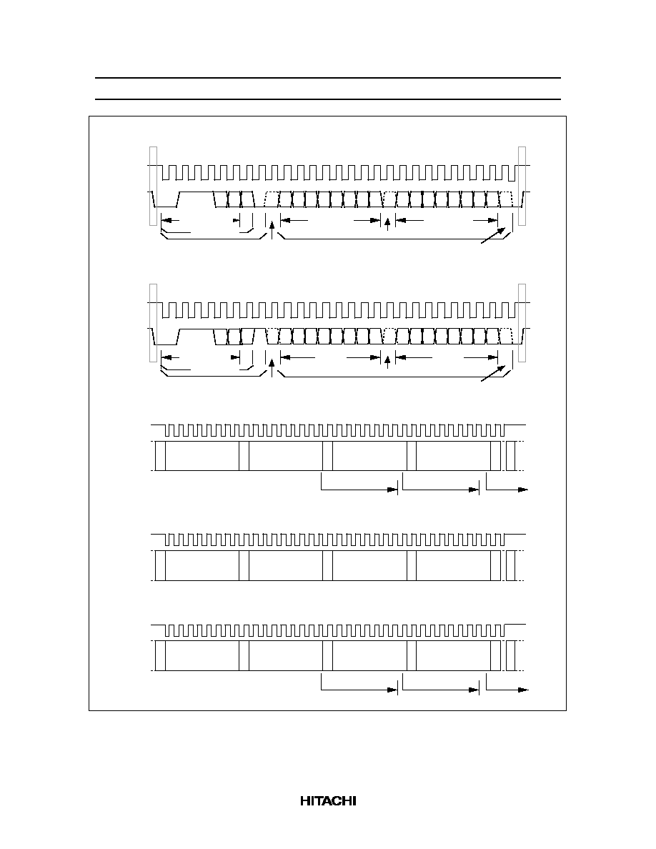
HD66727
48
a) Basic Data-Receive Timing through the I2C Bus Interface
1st byte
Instructions
Transfer end
1
2
3
4
5
6
7
8
9
10 11 12 13 14 15 16 17 18 19 20 21 22 23 24
D7 D6 D5 D4
0
0
1
1 1
0
1
1 1
2nd instruction
Device ID code
1st instruction
SCL
(Input)
SDA
(Input/
output)
ID0
ID1
ID0
ID1
RS
D3 D2 D1 D0
D7 D6 D5 D4 D3 D2 D1 D0
Transfer start
MSB
25 26
Ack
Ack
Ack
27
Acknowledge
RS
MSB
Slave address
R/
W
b) Basic Data-Transmit Timing through the I2C Bus Interface
1st byte
Instructions
Transfer end
1
2
3
4
5
6
7
8
9
10 11 12 13 14 15 16 17 18 19 20 21 22 23 24
D7 D6 D5 D4
1
2nd read
Device ID code
1st read
SCL
(Input)
SDA
(Input/
output)
RS
D3 D2 D1 D0
D7 D6 D5 D4 D3 D2 D1 D0
Transfer start
MSB
25 26
Ack
Ack
Ack
27
RS
MSB
Slave address
R/
W
1st byte
SCL
(Input)
SDA
(Input/
output)
d) Consecutive Key-Scanned Data-Transmit Timing through the I2C Bus Interface
S
1 2 3 4 5 6 7 8 9 10 11 12 13 14 15 16 17 18 19
Key-scanned data
(SCAN0)
A
C
K
A
C
K
A
C
K
20 21 22 23 24 25 26 27 28 29 30 31 32 33 34 35 36
A
C
K
P
Start
End
1st byte
RAM data 1
execution time
SCL
(Input)
SDA
(Input/
output)
e) Consecutive RAM Data-Transmit Timing through the I2C Bus Interface
S
1 2 3 4 5 6 7 8 9 10 11 12 13 14 15 16 17 18 19
RAM data 1
A
C
K
A
C
K
A
C
K
20 21 22 23 24 25 26 27 28 29 30 31 32 33 34 35 36
RAM data 2
execution time
A
C
K
P
Start
End
Transfers the RAM data-2 ACK after the RAM data 1 has been executed.
RAM data 2
RAM data 3
Key-scanned data
(SCAN1)
Key-scanned data
(SCAN2)
Transfers the ACK after 8-bit data has been transmitted.
1st byte
Instruction 1
execution time
SCL
(Input)
SDA
(Input/
output)
S
1 2 3 4 5 6 7 8 9 10 11 12 13 14 15 16 17 18 19
Instruction 1
A
C
K
A
C
K
Instruction 2
A
C
K
20 21 22 23 24 25 26 27 28 29 30 31 32 33 34 35 36
Instruction 2
execution time
Instruction 3
A
C
K
P
Start
End
Transfers the instruction-2 ACK after instruction 1 has been executed.
c) Consecutive Instruction-Receive Timing through the I2C Bus Interface
Acknowledge
Acknowledge
Acknowledge
Acknowledge
Acknowledge
Figure 23 I
2
C Bus Interface Timing Sequence

HD66727
49
Clock-Synchronized Serial Interface
Setting the IM pin (interface mode pin) to the high level allows standard clock-synchronized serial data
transfer, using the chip select line (CS*), serial data line (SDA), and serial transfer clock line (SCL).
The HD66727 initiates serial data transfer by transferring the start byte at the falling edge of the CS* input.
It ends serial data transfer at the rising edge of the CS* input.
Table 24 illustrates the first bytes of I
2
C bus interface data and Figure 24 shows the clock-synchronized
serial interface timing sequence.
The HD66727 is selected when the 6-bit chip address in the start byte transferred from the transmitting
device matches the 6-bit device identification code assigned to the HD66727. The HD66727, when
selected, receives the subsequent data string. The least significant bit of the identification code can be
determined by the ID0 pin. The upper five bits must be 01110. Two different chip addresses must be
assigned to a single HD66727 because the seventh bit of the start byte is used as a register select bit (RS):
when RS = 0, an instruction can be issued or key scan data can be read, and when RS = 1, data can be
written to or read from RAM. Read or write is selected according to the eighth bit of the start byte (R/W
bit) as shown in Table 27.
After receiving the start byte, the HD66727 receives or transmits the subsequent data byte-by-byte. Data is
transferred with the MSB first. To transfer data consecutively, adjust the data transfer rate so that the
HD66727 can complete the current instruction before the eighth bit of the next instruction is transferred
(see Table 23, Instruction List). If the next instruction is transferred during execution of the current
instruction, the next instruction will be ignored. Note that the display-clear instruction alone requires longer
execution time than the others.
Table 26
Start Byte of Clock-Synchronized Serial Interface Data
S
Bit 1
Bit 2
Bit 3
Bit 4
Bit 5
Bit 6
Bit 7
Bit 8
Transfer start
0
1
1
1
0
ID0
RS
R/W
Note:
Bits 1 to 6 indicate the device ID code.
Table 27
RS and R/W Bit Function of Clock-Synchronized Serial Interface Data
RS
R/W
Function
0
0
Writes instruction
0
1
Reads key scan data and BF flag
1
0
Writes RAM data
1
1
Reads RAM data
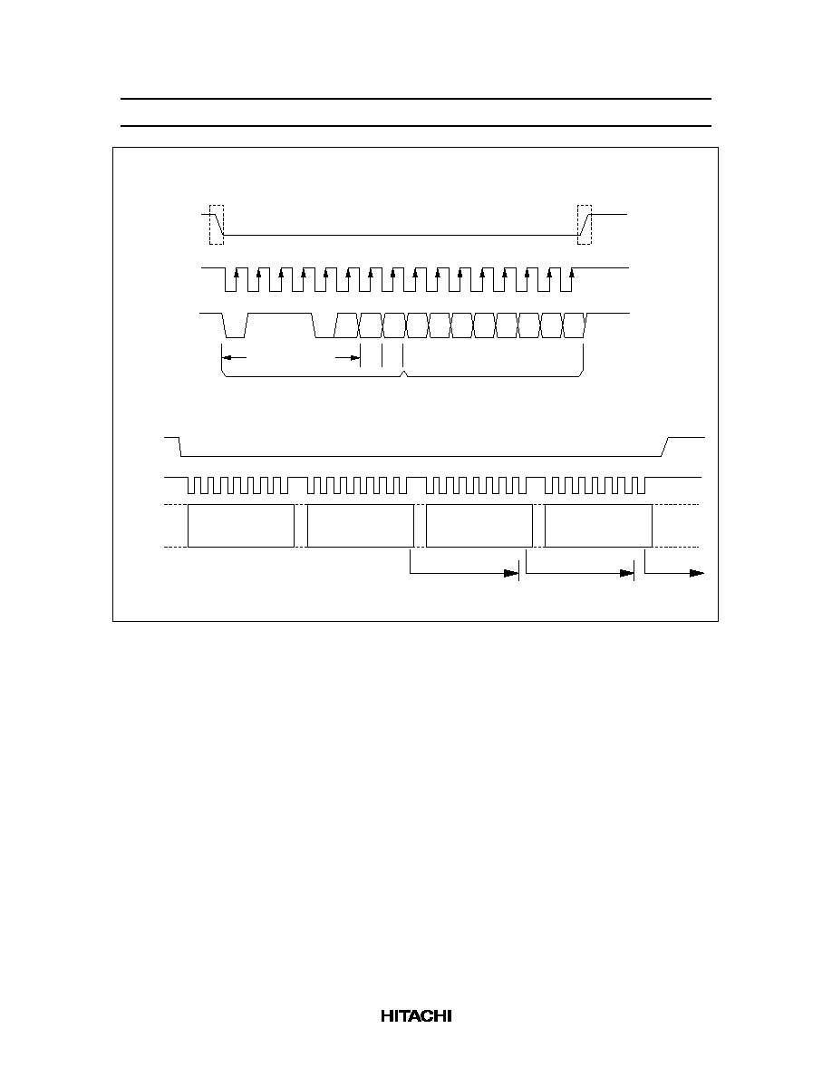
HD66727
50
Start byte
Instruction 1
execution time
SCL
(Input)
SDA
(Input/
output)
b) Consecutive Data-Transfer Timing through Clock-Synchronized Serial Bus Interface
1 2 3 4 5 6 7 8
9 10 11 12 13 14 15 16
17 18 19
Instruction 1
Instruction 2
20 21 22 23 24
25 26 27 28 29 30 31 32
Instruction 2
execution time
Instruction 3
Start
End
Adjust the transfer rate so that the HD66727 can complete
instruction 1 before the 8th bit of instruction 2 is transferred.
CS*
(Input)
1
Transfer start
a) Basic Data-Transfer Timing through Clock-Synchronized Serial Bus Interface
CS*
(Input)
SCL
(Input)
SDA
(Input/
Output)
2
3
4
5
6
7
8
9
10
11
12
13
14
15
"0" "1" "1" "1" "0" ID0 RS R/W
RS R/W
DB6 DB5 DB4 DB3 DB2 DB1 DB0
DB7
16
Transfer end
Device ID code
Instruction, RAM data,
key-scanned data
Start byte
MSB
LSB
Figure 24 Clock-Synchronized Serial Interface Timing Sequence

HD66727
51
Key Scan Control
Key Scan Mechanism
The key matrix scanner senses and holds the key states at each rising edge of the key strobe signals (KST)
that are output by the HD66727. The key strobe signals are output as time-multiplexed signals from KST0
to KST7. After passing through the key matrix, these strobe signals are used to sample the key state on four
inputs KIN0 to KIN3, enabling up to 32 keys to be scanned (Figure 25).
The states of inputs KIN0 to KIN3 are sampled by key strobe signal KST0 and latched into the SCAN0
register. Similarly, the data sampled by strobe signals KST1 to KST7 is latched into the SCAN1 to SCAN7
registers, respectively (Figure 26). Key pressing is stored as 1 in these registers.
The generation cycle and pulse width of the key strobe signals depend on the operating frequency
(oscillation frequency) of the HD66727, the display line determined by the NL1 bit, and the key scan cycle
determined by the KF0 and KF1 bits. For example, when the operating frequency is 160 kHz, NL1 is 1,
and KF0 and KF1 are both 0, the generation cycle is 8.0 ms and the pulse width is 1.0 ms (Figure 27).
When the operating frequency (oscillation frequency) is changed, the above generation cycle and the pulse
width are also changed in inverse proportion (Table 28).
Key matrix
Detail
Key state input
KST7
KST6
KST5
KST4
KST3
KST2
KST1
KST0
KIN0
KIN1
KIN2
KIN3
D23 D22 D21 D20
D33 D32 D31 D30
D03 D02 D01 D00
D13 D12 D11 D10
D43 D42 D41 D40
D53 D52 D51 D50
D63 D62 D61 D60
D73 D72 D71 D70
HD66727
Key strobe
Figure 25 Key Scan Configuration

HD66727
52
SCAN0
D03
D02
D01
D00
(KST0 )
KIN3 KIN2 KIN1 KIN0
SCAN1
D13
D12
D11
D10
(KST1 )
SCAN2
D23
D22
D21
D20
(KST2 )
SCAN3
D33
D32
D31
D30
(KST3 )
SCAN4
D43
D42
D41
D40
(KST4 )
SCAN5
D53
D52
D51
D50
(KST5 )
SCAN6
D63
D62
D61
D60
(KST6 )
SCAN7
D73
D72
D71
D70
(KST7 )
Figure 26 Key Scan Register Configuration
8.0 ms
Key scan cycle
1.0 ms
KST0
KST1
KST2
KST3
KST4
KST5
KST6
KST7
Figure 27 Key Strobe Output Timing (NL1 = 1, KF1/0 = 10, fcp/fosc = 160 kHz)
HD66727
53
Table 28
Key Scan Cycles for Each Operating Frequency
Register
Key Scan Cycle
NL1
KF1
KF0
Clock Cycle
160 kHz
120 kHz
80 kHz
40 kHz
0 (1, 2 lines)
0
0
160
(1.0 ms)*
(1.3 ms)*
2.0 ms
4.0 ms
0 (1, 2 lines)
0
1
320
(2.0 ms)*
(2.7 ms)*
4.0 ms
8.0 ms
0 (1, 2 lines)
1
0
640
(4.0 ms)*
(5.3 ms)*
8.0 ms
16.0 ms
0 (1, 2 lines)
1
1
1,280
(8.0 ms)*
(10.7 ms)*
16.0 ms
32.0 ms
1 (3, 4 lines)
0
0
320
2.0 ms
2.7 ms
(4.0 ms)*
(8.0ms)*
1 (3, 4 lines)
0
1
640
4.0 ms
5.3 ms
(8.0ms)*
(16.0ms)*
1 (3, 4 lines)
1
0
1,280
8.0 ms
10.7 ms
(16.0 ms)*
(32.0ms)*
1 (3, 4 lines)
1
1
2,560
16.0 ms
21.3 ms
(32.0 ms)*
(64.0ms)*
Note:
* Reference value
In order to compensate for the mechanical features of the keys, such as chattering and noise and for the
key-strobe generation cycle and the pulse width of the HD66727, software should read the scanned data
two or three times in succession to obtain valid data. Multiple keypress combinations should also be
processed in software. Up to three keys can be pressed simultaneously. Note, however, that if the third key
is pressed on an intersection between the rows and columns of the first two keys pressed, incorrect data will
be sampled. For three-key input, the third key must be on a separate column and row.
The input pins KIN0 to KIN3 are pulled up to V
CC
with internal MOS transistors (see the Electrical
Characteristics section). External resistors may also be required to further pull up the voltages when the
internal pull-ups are insufficient for the desired noise margins or for a large key matrix.
Key Scan Data Transfer
The key-scanned data can be read by an MPU via a serial interface as shown in Figure 28. First, a start byte
should be transferred. After the HD66727 has received the start byte, the MPU reads scan data SD0 to SD3
from the SCAN0 register starting from the MSB. Similarly, the MPU reads data from SCAN1, SCAN2,
SCAN3, SCAN4, SCAN5, SCAN6, and SCAN7 in that order. After reading SCAN7, the MPU starts at
SCAN0 again. While reading the scanned data, the MPU also reads the scan flags (SF1 and SF0) and the
transfer flag (TF). The scan flags reflect the value of the scan cycle counter, which automatically
increments its value by one for each scan cycle from 00 to 11 (after 11, it is reset to 00). If the scan data is
read more than once to be confirmed, and the corresponding scan counter values are the same, the scan data
might have been erroneously latched into the scan register at the same timing; it should be reconfirmed as
required. Also, if the transfer flag is read as 1, the HD66727 has been read out while it is latching scan data
and is thus unstable; it should also be reconfirmed as required.
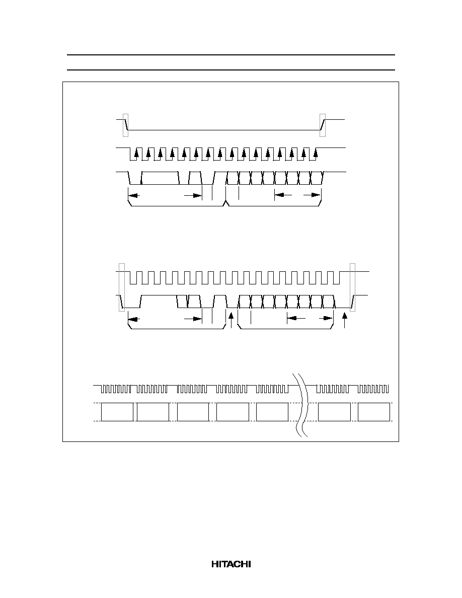
HD66727
54
c) Consecutive Scan Data Read Timing
a) Scan Data Read Timing through Clock-Synchronized Serial Bus Interface
1
2
3
4
5
6
7
8
9
10
11
12
13
14
15
16
R/W
RS
0
1
1
1
0
ID0
Start byte
Device ID code
SCL
(Input)
SDA
(Input/
output)
CS*
(Input)
Wait
Start
byte
SCL
(Input)
SDA
(Input/
output)
SCAN0
data
SCAN1
data
SCAN2
data
SCAN3
data
SCAN7
data
Wait
Wait
Wait
SCAN0
data
Wait
SCAN0 data transmission
BF
SD0
Busy
SF1 SF0 TF SD3 SD2 SD1
BF
SD0
SF1 SF0 TF SD3 SD2 SD1
Scan
flag
R/W
RS
Transfer start
Transfer end
0
1
1
1
ID1 ID0
b) Scan Data Read Timing through I2C Bus Interface
1
2
3
4
5
6
7
8
9
10
11
12
13
14
15
18
R/W
RS
1st byte
SCL
(Input)
SDA
(Input/
output)
SCAN0 data transmission
16
17
Ack
Ack
Transfer end
Transfer start
Acknowledge
Acknowledge
Busy
Scan
data
Device ID code
Scan
flag
R/W
RS
Scan
data
Figure 28 Scan Data Serial Transfer Timing
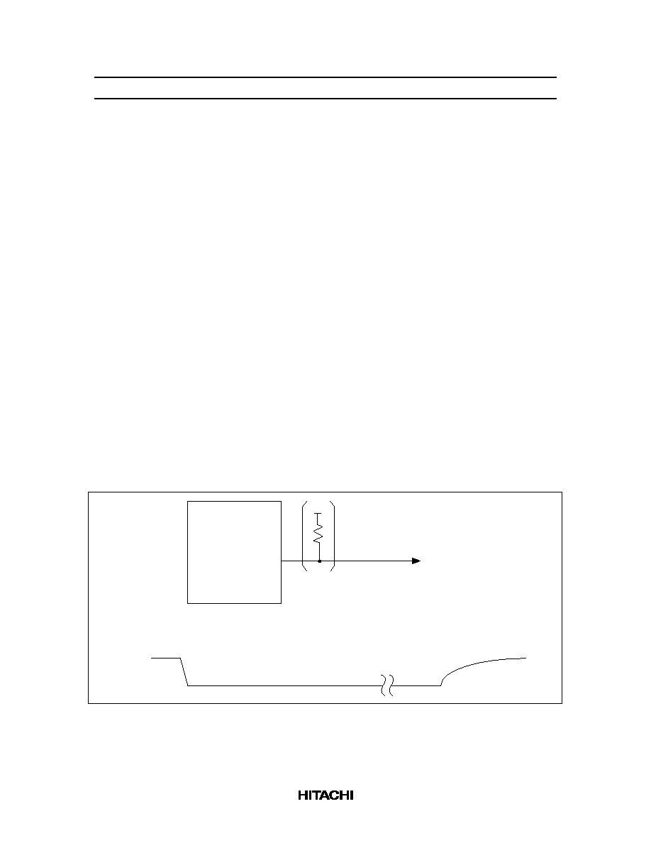
HD66727
55
Key Scan Interrupt (Wake-Up Function)
If the interrupt enable bit (IRE) is set to 1, the HD66727 sends an interrupt signal to the MPU on detecting
that a key has been pressed in the key scan circuit by setting the IRQ* output pin to a low level. An
interrupt signal can be generated by pressing any key in a 32-key matrix. The interrupt level continues to be
output during the key scan cycle in which the key is being pressed. See Figure 29.
Normal key scanning is performed and interrupts can occur in the HD66727 sleep mode (SLP = 1).
Accordingly, power consumption can be minimized in the sleep mode, where only annunciators can be
displayed, by triggering the MPU to read key states via the interrupt generated only when the HD66727
detects a key input from the 32-key matrix. For details, refer to the Sleep Mode section.
On the other hand, normal key scanning and the internal operating clock are halted in the standby mode
(STB = 1). During this period, the KST0 output is kept low, so the HD66727 can always sense four key
inputs D00 to D03, connected with KIN0 to KIN3, respectively. Therefore, if any of the four keys is
pressed in the standby mode, an interrupt occurs. Accordingly, power consumption can be further
minimized in the standby mode, where the whole system is inactive, by triggering the MPU via the
interrupt generated only when the HD66727 detects a key input from the above four keys. Note that the
interrupt generated in the standby mode automatically starts internal R-C oscillation. For details, refer to
the Standby Mode section.
The IRQ* output pin is pulled up to the V
CC
with an internal MOS resistor of approximately 50 k
;
additional external resistors may be required to obtain stronger pull-ups. Interrupts may occur if noise
occurs in KIN input during key scanning. Interrupts must be inhibited if not needed by setting the interrupt
enable bit (IRE) to 0.
Figure 30 shows key scan interrupt processing flow in sleep and standby modes.
IRQ
*
Interrupt generated
HD66727
IRQ
*
V
CC
MPU
Figure 29 Interrupt Generation
HD66727
56
Standby mode
Mask interrupts (IRE = 0)
Wait 10 ms or longer (MPU)
Start R-C oscillator (HD66727)
Clear standby mode (STB = 0)
Turn off LCD power (AMP = 0)
Set standby mode (STB = 1)
Generate interrupt (HD66727
Read key-scanned data
Enable interrupts (IRE = 1)
Turn off LCD power (AMP = 0)
Set sleep mode (SLP = 1)
Key input (key
HD66727)
Generate interrupt (HD66727
MPU)
Sleep mode
Mask interrupts (IRE = 0)
Read key-scanned data
Enable interrupts (IRE = 1)
HD66727)
Key input (key
MPU)
(1) Sleep Mode
(2) Standby Mode
Figure 30 Key Scan Interrupt Processing Flow in Sleep and Standby Modes
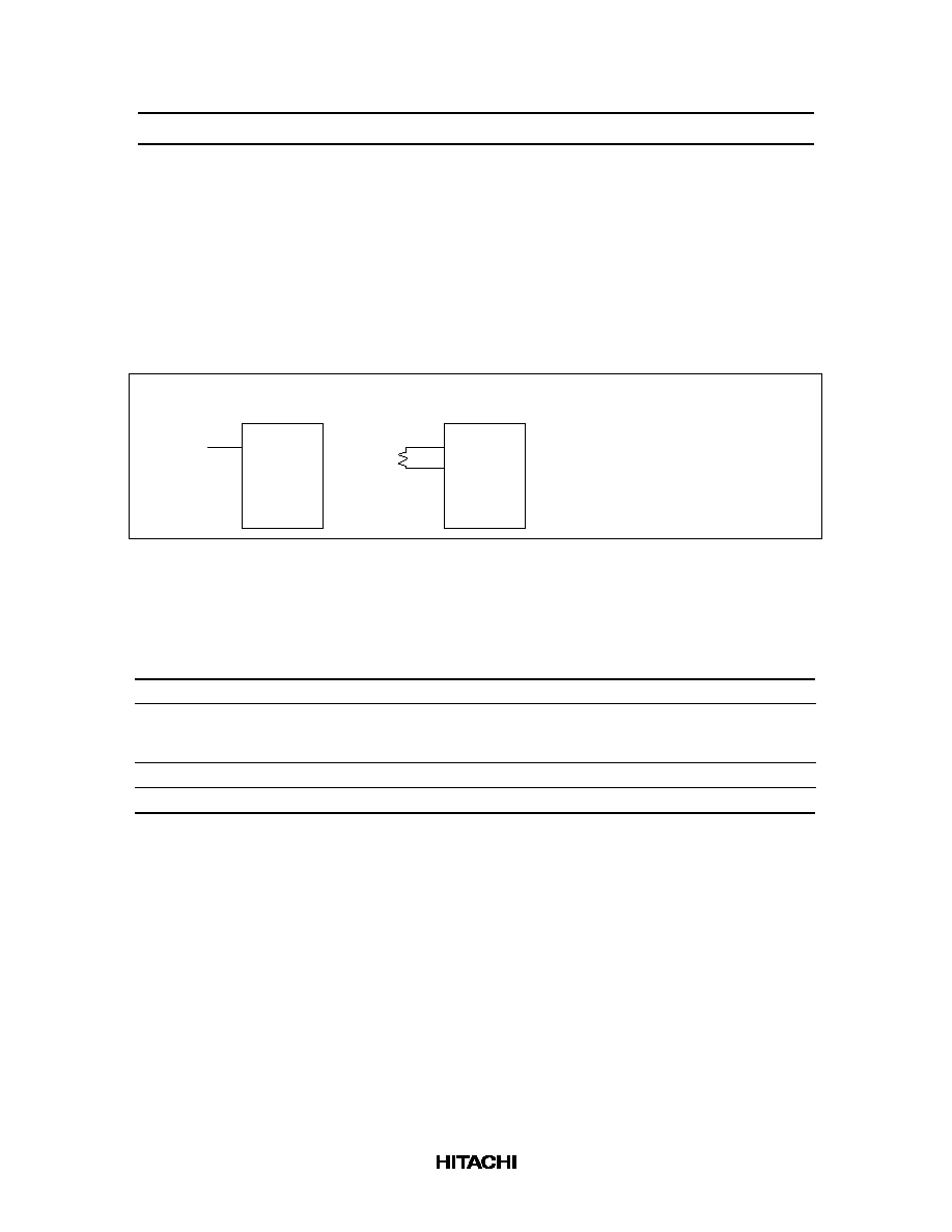
HD66727
57
Oscillator Circuit
The HD66727 can either be supplied with operating clock pulses externally (external clock mode) or
oscillate using an internal R-C oscillator and an external oscillator-resistor (internal oscillation mode), as
shown in Figure 31. An appropriate oscillator-resistor must be used to obtain the optimum clock frequency
according to the number of display lines (Table 29). Instruction execution times change in proportion to the
operating clock frequency or R-C oscillation frequency; MPU data transfer rate must be appropriately
adjusted (see Table 23, Instruction List). Figure 32 shows a sample LCD drive output waveform, where 4-
lines are displayed with 1/34 multiplexing duty ratio.
OSC1
OSC1
OSC2
Clock
Rf
The oscillator frequency can be
adjusted by oscillator resistance
(Rf). If Rf is increased or power
supply voltage is decreased, the
oscillator frequency decreases.
HD66727
1) When an external clock is used
2) When an internal oscillator is used
HD66727
Figure 31 Oscillator Circuit
Table 29
Oscillation Frequency and LCD Frame Frequency
Item
1-Line Display
(NL1, NL0 = 00)
2-Line Display
(NL1, NL0 = 01)
3-Line Display
(NL1, NL0 = 10)
4-Line Display
(NL1, NL0 = 11)
Multiplexing duty ratio
1/10
1/18
1/26
1/34
R-C oscillation
frequency
(recommended value)
40 kHz
80 kHz
120 kHz
160 kHz
1-line drive frequency
0.66 kHz
1.3 kHz
2.0 kHz
2.7 kHz
Frame frequency
67 Hz
74 Hz
77 Hz
78 Hz

HD66727
58
1
2
3
4
33
34
1
2
3
33
34
V
CC
V1
V4
V5
COM1
1-line selection period
V1
V4
V5
COM2
1 frame
V
CC
V1
V4
V5
COMS2
V
CC
V1
V4
V5
COMS1
V
CC
1 frame
Figure 32 LCD Drive Output Waveform Example (4-line display with 1/34 multiplexing duty ratio)

HD66727
59
Power Supply for Liquid Crystal Display Drive
When External Power Supply and Internal Operational Amplifiers are Used
To supply LCD drive voltage directly from the external power supply without using the internal booster,
circuits should be connected as shown in Figure 33. Here, contrast can be adjusted through the CT bits of
the contrast control instruction.
The HD66727 incorporates a voltage-follower operational amplifier for each of V1 to V5 to reduce current
flowing through the internal bleeder-resistors, which generate different levels of liquid-crystal drive
voltages. Thus, potential differences between V
CC
and V1 and between V
EE
and V5 must be 0.4V or greater.
Note that the OPOFF pin must be grounded when using the operational amplifiers.
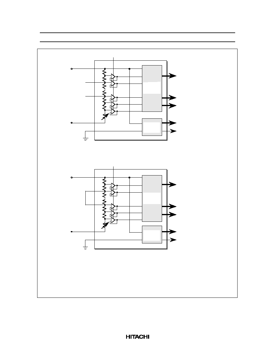
HD66727
60
V
CC
V2
V3
V
CC
R
V1
V2
V3
V4
V5
R
R
R
R
V
EE
VR
-
+
-
+
-
+
-
+
R
SEG1≠SEG60
COM1≠COM32
COMS1≠COMS2
GND
AGND
Open
ASEG1≠ASEG12
ACOM
-
+
V
EE
HD66727
OPOFF = GND
a) 3- or 4-line display with 1/6 bias
b) 1- or 2-line display with 1/4 bias
Notes: 1. Potential differences between V
CC
and V1 and between V5 and V
EE
must be 0.4V or greater,
particularly for low-duty drive such as 1-line display.
2. When the internal operational amplifiers cannot fully drive the LCD panel used, an appropriate
capacitor must be inserted between each output of V1OUT to V5OUT and V
CC
to stabilize the
operational amplifier output.
V
CC
V2
V3
V
CC
R
R
R
R
R
V
EE
VR
-
+
-
+
-
+
-
+
R
SEG1≠SEG60
COM1≠COM16
COMS1≠COMS2
GND
AGND
ASEG1≠ASEG12
ACOM
Short-circuited
-
+
V
EE
HD66727
OPOFF = GND
LCD
multiplexing
driver
LCD static
driver
LCD
multiplexing
driver
LCD static
driver
V1
V2
V3
V4
V5
Figure 33 External Power Supply Circuit Example for LCD Drive Voltage Generation

HD66727
61
When an Internal Booster and Internal Operational Amplifiers are Used
To supply LCD drive voltage using the internal booster, circuits should be connected as shown in Figure
34. Here, contrast can be adjusted through the CT bits of the contrast control instruction. Temperature can
be compensated either through the CT bits or by controlling the reference voltage for the booster (Vci pin)
using a thermistor.
Note that Vci is both a reference voltage and power supply for the booster; the reference voltage must
therefore be adjusted using an emitter-follower or a similar element so that sufficient current can be
supplied. In this case, Vci must be equal to or smaller than the V
CC
level.
The HD66727 incorporates a voltage-follower operational amplifier for each of V1 to V5 to reduce current
flowing through the internal bleeder-resistors, which generate different levels of liquid-crystal drive
voltages. Thus, potential differences between V
CC
and V1 and between V
EE
and V5 must be 0.4V or greater.
Note that the OPOFF pin must be grounded when using the operational amplifiers.

HD66727
62
Short-circuited
for 1-or 2-line
display
b) Triple boosting
C1
C2
Vci
V5OUT2
V5OUT3
+
GND
+
V
CC
V2
V3
V
CC
R
V1
V2
V3
V4
V5
R
R
R
R
VR
≠
+
≠
+
≠
+
≠
+
R
≠
+
V
EE
Booster
GND
+
OPOF = GND
0.47
µ
F
to 1
µ
F
0.47
µ
F
to 1
µ
F
HD66727
Notes: 1. The reference voltage input (Vci) must be adjusted so that the output voltage after boosting will not exceed
the absolute maximum rating of the liquid-crystal power supply voltage (15V). Particularly, Vci must be
5V or less for triple boosting.
2. Vci is both a reference voltage and power supply for the booster; connect it to V
CC
directly or combine it with
a transistor so that sufficient current can be obtained.
3. Vci must be smaller than V
CC
.
4. To operate the voltage-follower correctly, potential differences between V
CC
and V1 and between V5 and
V
EE
must be 0.4V or greater, particularly for low-duty drive such as 1-line display.
5. Polarized capacitors must be connected correclty.
6. Circuits for temperature compensation should be designed based on the sample circuit shown in figure 35.
7. The HD66727's internal operational amplifiers have a reduced drive current to save current consumption;
when the internal operational amplifiers cannot fully drive the LCD panel used, an appropriate capacitor must
be inserted between each output of V1OUT to V5OUT and V
CC
to stabilize the operational amplifier output
(Figure 36).
a) Double boosting
C1
C2
Vci
V5OUT2
V5OUT3
+
GND
+
V
CC
V2
V3
V
CC
R
R
R
R
R
VR
R
V
EE
Short-circuited
for 1-or 2-line
display
OPOFF = GND
-
+
-
+
-
+
-
+
-
+
C1
C2
Vci
V5OUT2
V5OUT3
+
GND
+
V2
V3
V
R
R
R
R
R
VR
R
Booster
0.47
µ
F
to 1
µ
F
0.47
µ
F
to 1
µ
F
HD66727
≠
+
≠
+
≠
+
≠
+
≠
+
V1
V2
V3
V4
V5
Figure 34 Internal Power Supply Circuit Example for LCD Drive Voltage Generation
V
CC
Thermistor
GND
Tr
V
CC
Vci
HD66727
Figure 35 Temperature Compensation Circuit Example
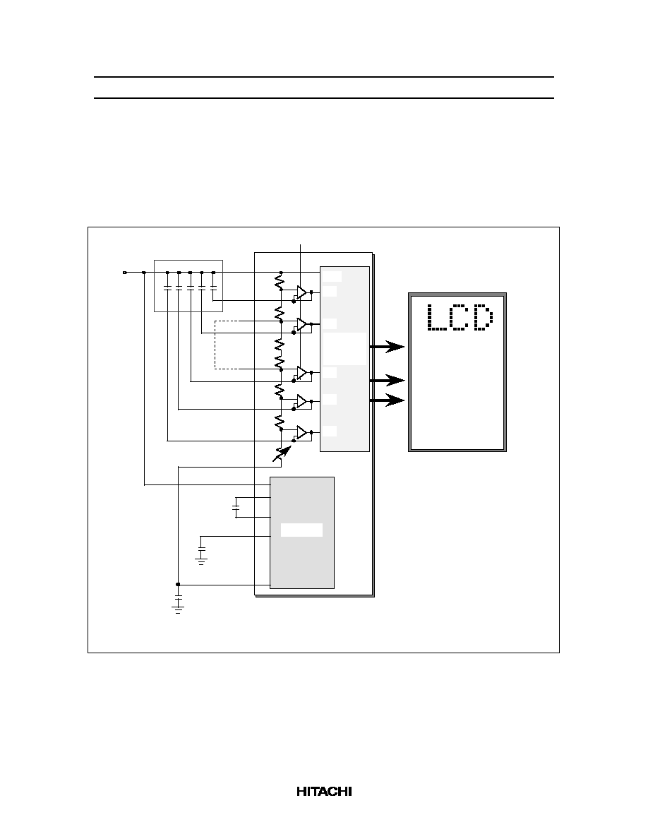
HD66727
63
Example of Using Internal Operational Amplifier when Driving Large Size of LCD
The driving current of the internal operational amplifier in the HD66727 is reduced to control the
consumption current. When load current is apparently large such as when driving large size of LCD panel,
insert a capacitor between V1OUT≠V5OUT outputs and V
CC
power supply, and stabilize the output level of
the operational amplifier. Especially the capacitors for V1OUT and V4OUT must be inserted when 1/26
duty or 1/34 duty drives.
C1
C2
Vci
V5OUT2
V5OUT3
+
GND
+
V
CC
V2
V3
V
CC
R
R
R
R
VR
≠
+
≠
+
≠
+
≠
+
≠
+
V
EE
Booster
+
0.47
µ
F
to 1
µ
F
0.47
µ
F
to 1
µ
F
0.47
µ
F
to 1
µ
F
OPOFF = GND
Large size of LCD panel
V5OUT3
V2
R
R
GND
+
HD66727
V1OUT
+
V2OUT
V3OUT
V4OUT
V5OUT
+
+
+
+
SEG1≠SEG60
COM1≠COM16
COMS1≠COMS2
LCD
multiplexing
driver
V
CC
V1
V2
V3
V4
V5
Note : The capacitors for V1OUT and V4OUT must be inserted when 1/26 duty or 1/34 duty drives.
0.1
µ
F to 0.5
µ
F*
Figure 36 Operational Amplifier Output Stabilization Circuit Example when Driving Large Size of
LCD Panel

HD66727
64
LCD driving current (I
EE
)
*
2
When 1/10, 1/18-duty drive
(1 line, 2 lines)
When 1/26, 1/34-duty drive
(3 lines, 4 lines)
When I
EE
15
µ
A
Capacitors for V1OUT to V5OUT
must be inserted.
Capacitors for V1OUT to V5OUT
must be inserted.
When 15
µ
A
I
EE
40
µ
A
Capacitors for V1OUT and V4OUT
must be inserted.
Capacitors for V1OUT and V4OUT
must be inserted.
When I
EE
40
µ
A
Capacitors for V1OUT and V4OUT
may be inserted after confirming the
display quality.
And additional capacitors for other
VnOUTs may be inserted after
confirming the display quality.
Notes: 1. These relationships between LCD driving current (I
EE
) and the external capacitors are applied to
designing LCM, but they cannot guarantee the practical display quality. This display quality
depends on LCD panel size and LCD material used, and it must be checked and confirmed with
your LCD panel.
2. These LCD driving currents (I
EE
) depend on the LCD driving voltage between V
CC
and V
EE
, and
setting of VREF, VREFP and VREFP pins.
3. Especially the capacitors for V1OUT and V4OUT are most efficient for display quality.
4. This condition is an example when the frame frequency is 60Hz to 100Hz. If higher frame
frequency is used, these external capacitors should be enhanced to prevent the cross-talk.
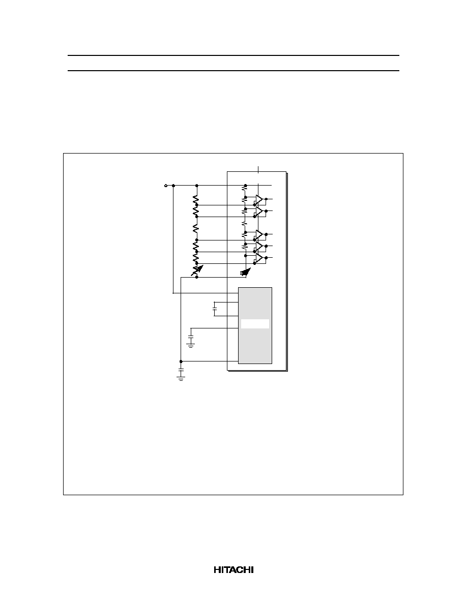
HD66727
65
When an Internal Booster and External Bleeder-Resistors are Used
When the internal operational amplifiers cannot fully drive the LCD panel used, V1 to V5 voltages can be
supplied through external bleeder-resistors (Figure 37). Here, the OPOFF pin must be set to the V
CC
level to
turn off the internal operational amplifiers. Since the internal contrast adjuster is disabled in this case,
contrast must be adjusted externally. Double- and triple-boosters can be used as they are.
C1
C2
Vci
V5OUT2
V5OUT3
+
GND
+
V
CC
V1OUT
V2OUT
V3OUT
V4OUT
V5OUT
V
CC
Notes: 1. Resistance of each external bleeder resistor should be 5 k
to 15 k
.
2. The bias current value for driving liquid-crystals can be varied by adjusting
the resistance (2R) between the V2OUT and V3OUT pins.
3. The internal contrast-adjuster is disabled; contrast must be adjusted either
by controlling the external variable resistor between V
EE
and V5OUT or Vci
for the booster.
4. Vci is both a reference voltage and power supply for the booster; connect it to
V
CC
directly or combine it with a transistor so that sufficient current can be
obtained.
5. Vci must be smaller than V
CC
.
≠
+
≠
+
≠
+
≠
+
≠
+
V
EE
Booster
GND
+
0.47
µ
F
to 1
µ
F
0.47
µ
F
to 1
µ
F
0.47
µ
F
to 1
µ
F
HD66727
OPOFF = V
CC
R
R
R
R
VR
2R
V
CC
V1
V2
V3
V4
V5
Figure 37 Power Supply Circuit Example Using External Bleeder-Resistor for LCD Drive Voltage
Generation

HD66727
66
Contrast Adjuster
Multiplexing Drive System
Contrast for an LCD controlled by the multiplexing drive method can be adjusted by varying the liquid-
crystal drive voltage (potential difference between V
CC
and V5) through the CT bits of the contrast control
instruction (electron volume function). See Figure 38 and Table 30. The value of a variable resistor (VR)
can be adjusted within the range from 0.4 x R through 6.4 x R, where R is a reference resistance obtained
by dividing the total resistance between V
CC
and V5.
The HD66727 incorporates a voltage-follower operational amplifier for each of V1 to V5 to reduce current
flowing through the internal bleeder-resistors, which generate different levels of liquid-crystal drive
voltages. Thus, potential differences between V
CC
and V1 and between V
EE
and V5 must be 0.4V or greater.
Note that the OPOFF pin must be grounded when using the operational amplifiers.
1/6 bias (V2 and V3 pins left open):
LCD drive voltage VLCD: 6R
◊
(V
CC
≠ V
EE
)/(6R + VR) (VR = a value within the range from 0.4R to
6.4R)
VLCD adjustable range: 0.484
◊
(V
CC
≠ V
EE
)
VLCD
0.938
◊
(V
CC
≠ V
EE
)
Potential difference between V
CC
and V1: R
◊
(V
CC
≠ V
EE
)/(6R + VR)
0.4 (V)
Potential difference between V5 and V
EE
: VR
◊
(V
CC
≠ V
EE
)/(6R + VR)
0.4 (V)
1/4 bias (V2 and V3 pins short-circuited):
LCD drive voltage VLCD: 4R
◊
(V
CC
≠ V
EE
)/(4R + VR) (VR = a value within the range from 0.4R to
6.4R)
VLCD adjustable range: 0.385
◊
(V
CC
≠ V
EE
)
VLCD
0.909
◊
(V
CC
≠ V
EE
)
Potential difference between V
CC
and V1: R
◊
(V
CC
≠ V
EE
)/(4R + VR)
0.4 (V)
Potential difference between V5 and V
EE
: VR
◊
(V
CC
≠ V
EE
)/(4R + VR)
0.4 (V)

HD66727
67
V
CC
V
CC
V2
V3
R
V1
CT
V2
V3
V4
V5
R
R
R
R
VR
≠
+
≠
+
≠
+
≠
+
R
≠
+
V
EE
HD66727
Figure 38 Contrast Adjuster
Table 30
Contrast-Adjust Bits (CT) and Variable Resistor Values
CT3
CT2
CT1
CT0
Variable Resistor Value (VR)
0
0
0
0
6.4 R
0
0
0
1
6.0 R
0
0
1
0
5.6 R
0
0
1
1
5.2 R
0
1
0
0
4.8 R
0
1
0
1
4.4 R
0
1
1
0
4.0 R
0
1
1
1
3.6 R
1
0
0
0
3.2 R
1
0
0
1
2.8 R
1
0
1
0
2.4 R
1
0
1
1
2.0 R
1
1
0
0
1.6 R
1
1
0
1
1.2 R
1
1
1
0
0.8 R
1
1
1
1
0.4 R
Static Drive System
Contrast for a statically-driven LCD, that is, annunciator display, can be adjusted through the AGND pin.
The annunciators are driven statically by the potential difference between V
CC
and AGND. The AGND pin
level must be equal to or greater than the GND level.

HD66727
68
LCD Panel Interface
The HD66727 can change the shift direction of common drivers COM1≠COM32 and COMS1 and COMS2
and segment drivers SEG1≠SEG60 with the CMS and SGS bits. These bits can be selected according to the
mounting method such as the chip arrangement or wire leading. However, the output position of
annunciator drivers ASEG1≠ASEG12 cannot be changed, so adjust it by software.
HITACHI LTD.
new HD66727
LCD CONTROLL
with KeyScan
Front of chip
COM32/1
COM16/17
SEG60/1
COM1/32
HITACHI LTD.
new HD66727
LCD CONTROLL
with KeyScan
Back of chip
COM16/17
COM32/1
SEG1/60
COM17/16
b) Back of chip(CMS = "1" SGS = "0")
a) Front of chip (CMS = "1" SGS = "1")
HITACHI LTD.
new HD66727
LCD CONTROLL
with KeyScan
Front of chip
COM16/17
COM17/16
SEG1/60
COM32/1
HITACHI LTD.
new HD66727
LCD CONTROLL
with KeyScan
Back of chip
COM32/1
COM1/32
SEG60/1
COM16/17
b) Back of chip(CMS = "0" SGS = "1")
a) Front of chip(CMS = "0" SGS = "0")
Figure 39 LCD Module Interface Examples

HD66727
69
Segment Display and Annunciator Display
The HD66727 provides both segment display, which is driven by the multiplexing method, and annunciator
display, which is driven statically. Annunciator display is driven at a logic operating voltage (V
C C
≠
AGND) and is thus also available while the LCD drive power supply is turned off. Accordingly,
annunciator display is suitable for displaying marks during system standby, when it is desirable to reduce
current consumption. It is available in the sleep mode, where internal multiplexing operations for character
or segment display are halted. If an alternating signal is supplied to the EXM pin, it is also available in the
standby mode, where the internal R-C oscillator is halted. Here, AGND must be equal to or above the GND
level.
Note that annunciator display cannot share character display drivers SEG and COM but require special
drivers ASEG and ACOM that require long routing.
Tables 31 to 34 compare segment display to annunciator display. Figure 40 shows annunciator drive output
waveforms in two modes.
Table 31
Comparison between Segment Display and Annunciator Display
Item
Segment Display
Annunciator Display
Number of driven elements
40 each by 5-dot font width
48 each by 6-dot font width
12
Blinking
Impossible
Possible
Segment drivers
SEG1≠SEG60
(shared with character display)
ASEG1≠ASEG12
(independent of character display)
Common drivers
COMS1, COMS2
ACOM
LCD power supply
V
CC
≠ V5
(LCD power supply necessary)
V
CC
≠ AGND
(LCD power supply unnecessary)
Normal mode display
Possible together with
character display by multiplexing
drive
Possible by static drive
Sleep mode display
Impossible
(SEG and COM output V
CC
)
Possible by static drive
Standby mode display
(without oscillation)
Impossible
(SEG and COM output V
CC
)
Possible by supplying alternating
signal to the EXM pin

HD66727
70
Table 32
Correspondence between Segment Display SEGRAM Addresses (ASEG) and Driver
Signals when 5-Dot Font Width
ASEG Address
Common
Segment Signal
MSB
LSB
Signal
Bit 4
Bit 3
Bit 2
Bit 1
Bit 0
1
0
0
0
COMS1
SEG1/21/41
SEG2/22/42
SEG3/23/43
SEG4/24/44
SEG5/25/45
1
0
0
1
COMS1
SEG6/26/46
SEG7/27/47
SEG8/28/48
SEG9/29/49
SEG10/30/50
1
0
1
0
COMS1
SEG11/31/51
SEG12/32/52
SEG13/33/53
SEG14/34/54
SEG15/35/55
1
0
1
1
COMS1
SEG16/36/56
SEG17/37/57
SEG18/38/58
SEG19/39/59
SEG20/40/60
1
1
0
0
COMS2
SEG1/21/41
SEG2/22/42
SEG3/23/43
SEG4/24/44
SEG5/25/45
1
1
0
1
COMS2
SEG6/26/46
SEG7/27/47
SEG8/28/48
SEG9/29/49
SEG10/30/50
1
1
1
0
COMS2
SEG11/31/51
SEG12/32/52
SEG13/33/53
SEG14/34/54
SEG15/35/55
1
1
1
1
COMS2
SEG16/36/56
SEG17/37/57
SEG18/38/58
SEG19/39/59
SEG20/40/60
Table 33
Correspondence between Segment Display SEGRAM Addresses (ASEG) and Driver
Signals when 6-Dot Font Width
ASEG Address
Common
Segment Signal
MSB
LSB
Signal
Bit 7
Bit 6
Bit 5
Bit 4
Bit 3
Bit 2
Bit 1
Bit 0
1
0
0
0
COMS1
*
*
SEG1/25/
49
SEG2/26/
50
SEG3/27/
51
SEG4/28/
52
SEG5/29/
53
SEG6/30/
54
1
0
0
1
COMS1
*
*
SEG7/31/
55
SEG8/32/
56
SEG9/33/
57
SEG10/
34/58
SEG11/
35/59
SEG12/
36/60
1
0
1
0
COMS1
*
*
SEG13/
37
SEG14/
38
SEG15/
39
SEG16/
40
SEG17/
41
SEG18/
42
1
0
1
1
COMS1
*
*
SEG19/
43
SEG20/
44
SEG21/
45
SEG22/
46
SEG23/
47
SEG24/
48
1
1
0
0
COMS2
*
*
SEG1/25/
49
SEG2/26/
50
SEG3/27/
51
SEG4/28/
52
SEG5/29/
53
SEG6/30/
54
1
1
0
1
COMS2
*
*
SEG7/31/
55
SEG8/32/
56
SEG9/33/
57
SEG10/
34/58
SEG11/
35/59
SEG12/
36/60
1
1
1
0
COMS2
*
*
SEG13/
37
SEG14/
38
SEG15/
39
SEG16/
40
SEG17/
41
SEG18/
42
1
1
1
1
COMS2
*
*
SEG19/
43
SEG20/
44
SEG21/
45
SEG22/
46
SEG23/
47
SEG24/
48

HD66727
71
Table 34
Correspondence between Annunciator Display Addresses (AAN) and Driver Signals
AAN Address
Segment Signal
MSB
LSB
Common Signal
Bits 7, 6
Bits 5, 4
Bits 3, 2
Bits 1, 0
0
0
0
0
ACOM
ASEG1
ASEG2
ASEG3
ASEG4
0
0
0
1
ACOM
ASEG5
ASEG6
ASEG7
ASEG8
0
0
1
0
ACOM
ASEG9
ASEG10
ASEG11
ASEG12
Note:
The annunciator is turned on when the corresponding even bit (bit 6, 4, 2, or 0) is 1, and the turned-
on annunciator blinks when the corresponding odd bit (bit 7, 5, 3, or 1) is 1.
i) Normal mode and sleep mode
ii) Standby mode (without oscillation)
V
CC
level
V
CC
level
V
CC
level
AGND level
AGND level
AGND level
AGND level
AGND level
V
CC
level
V
CC
level
V
CC
level
V
CC
level
Display off
Display on
1 frame
ACOM
ASEG1
ASEG2
EXM
(Input)
V
CC
level
V
CC
level
V
CC
level
AGND level
AGND level
AGND level
V
CC
level
V
CC
level
V
CC
level
ACOM
ASEG1
ASEG2
Display off
Display on
1 frame
Note: If annunciator display is unnecessary during standby mode, make sure to fix the EXM pin to the V
CC
or GND level
and set the annunciator display ON bit (DA) to 0. This will prevent dark display and liquid-cell deterioration due to
DC bias application on liquid crystal cells.
Figure 40 Annunciator Drive Output Waveforms

HD66727
72
Vertical Smooth Scroll
The HD66727 can scroll in the vertical direction in units of raster-rows. This function is achieved by
writing character codes into DDRAM area that is not being used for display. In other words, since DDRAM
corresponds to a 5-line
◊
12-character display, one of the lines can be used to achieve continuous smooth
vertical scroll even in a 4-line display. Here, after the fifth line is displayed, the first line is displayed again.
Specifically, this function is controlled by incrementing or decrementing the value in the display-start line
bits (SL2 to SL0) and display-start raster-row bits (SN2 to SN0) by 1. For example, to smoothly scroll up,
first set SN2 to SN0 to 000, and increment SL2 to SL0 by 1 from 000 to 111 to scroll seven raster-rows.
Then increment SN2 to SN0 to 001, and again increment SL2 to SL0 by 1 from 000 to 111. To start
displaying and scrolling from the first raster-row of the second line, update the first line of DDRAM data as
desired during its non-display period.
Figure 41 shows an example of vertical smooth scrolling and Figure 42 shows an example of setting
instructions for vertically scrolling upward in a 4-line display (NL1 and NL0 = 11).
HD66727
73
Update the first line of DDRAM data
9) 8 raster-rows scrolled
up
∑ SN2≠SN0 = 001
∑ SL2≠SL0 = 000
Set initial data to all DDRAM addresses
1) Not scrolled
∑ SN2≠0 = 000
∑ SL2≠0 = 000
2) 1 raster-rows scrolled
up
∑ SL2≠SL0 = 001
3) 2 raster-rows scrolled
up
∑ SL2≠SL0 = 010
4) 3 raster-rows scrolled
up
∑ SL2≠SL0 = 011
5) 4 raster-rows scrolled
up
∑ SL2≠SL0 = 100
6) 5 raster-rows scrolled
up
∑ SL2≠SL0 = 101
7) 6 raster-rows scrolled
up
∑ SL2≠SL0 = 110
10) 9 raster-rows scrolled
up
∑ SL2≠SL0 = 001
11) 10 raster-rows scrolled
up
∑ SL2≠SL0 = 010
12) 11 raster-rows scrolled
up
∑ SL2≠SL0 = 011
13) 12 raster-rows scrolled
up
∑ SL2≠SL0 = 100
14) 13 raster-rows scrolled
up
∑ SL2≠SL0 = 101
15) 14 raster-rows scrolled
up
∑ SL2≠SL0 = 110
16) 15 raster-rows scrolled
up
∑ SL2≠SL0 = 111
8) 7 raster-rows scrolled
up
∑ SL2≠SL0 = 111
Figure 41 Example of Vertical Smooth Scrolling
HD66727
74
DB7 DB6 DB5 DB4 DB3 DB2 DB1 DB0
R/W RS
0
0
0
0
1
0
CT
SN2= 0
0
0
0
1
0
0
SN1/0 = 00 and SL2≠SL0 = 000
(1st raster-row of 1st line displayed at the top)
0
0
1
CPU Wait
Scroll up 1 raster-row
(2nd raster-row of 1st line displayed at the top)
0
0
0
0
1
0
1
0
0
1
0
CPU Wait
Scroll up 2 raster-rows
(3rd raster-row of 1st line displayed at the top)
0
0
0
1
1
0
0
0
1
0
CPU Wait
Scroll up 3 raster-rows
(4th raster-row of 1st line displayed at the top)
0
0
0
1
1
1
0
0
1
0
CPU Wait
Scroll up 4 raster-rows
(5th raster-row of 1st line displayed at the top))
0
0
0
1
0
0
1
0
1
0
CPU Wait
Scroll up 7 raster-rows
(8th raster-row of 1st line displayed at the top)
0
0
0
1
1
1
1
1
0
CPU Wait
Scroll up 8 raster-rows
(1st raster-row of 2nd line displayed at the top)
(While 1st line is not being displayed but
2nd to 5th lines are being displayed)
(While 2nd line is not being displayed but
1st and 3rd to 5th lines are being displayed)
0
0
0
1
0
0
0
1
1
0
CPU Wait
Scroll up 9 raster-rows
(2nd raster-row of 2nd line displayed at the top)
0
0
0
1
0
1
0
1
1
0
CPU Wait
Scroll up 15 raster-rows
(8th raster-row of 2nd line displayed at the top)
0
0
0
1
1
1
1
1
1
0
CPU Wait
Scroll up 16 raster-rows
(1st raster-row of 3rd line displayed at the top)
0
0
0
1
0
0
0
0
1
1
CPU Wait
Scroll up 17 raster-rows
(2nd raster-row of 3rd line displayed at the top)
0
0
0
1
0
1
0
0
1
1
Scroll up display
Set initial character codes of 5 lines to all DDRAM addresses
Update 1st-line (address 00H to 1BH) character codes in DDRAM
Update 2nd-line (address 10H to 1BH) character codes in DDRAM
0
Figure 42 Example of Setting Instructions for Vertical Smooth Scroll
(4-line display (NL1 and NL0 = 11))

HD66727
75
Line-Cursor Display
The HD66727 can assign a cursor attribute to an entire line corresponding to the address counter value by
setting the LC bit to 1 (Table 35). One of three line-cursor modes can be selected: a black-white inverting
blink cursor (B/W = 1), an underline cursor (C = 1), and a blink cursor (B = 1). The blink cycle for a black-
white inverting cursor and for a blink cursor is 32 frames. These line-cursors are suitable for highlighting
an index and/or marker, and for indicating an item in a menu with a cursor or an underline.
Figures 43 to 45 show three line-cursor examples.
Table 35
Address Counter Value and Line-Cursor
Address Counter Value (AC)
Selected Line for Line-Cursor
"00"H to "0B"H
Entire 1st line (12 characters)
"10"H to "1B"H
Entire 2nd line (12 characters)
"20"H to "2B"H
Entire 3rd line (12 characters)
"30"H to "3B"H
Entire 4th line (12 characters)
"40"H to "4B"H
Entire 5th line (12 characters)

HD66727
76
Alternates every 32 frames
Figure 43 Example of Black-White Inverting Blink Cursor (LC = 1; B/W = 1)
HD66727
77
Figure 44 Example of Underline Cursor (LC = 1; C = 1)
HD66727
78
Alternates every 32 frames
Figure 45 Example of Blink Cursor (LC = 1; B = 1)

HD66727
79
Double-Height Display
The HD66727 can double the height of any desired line from the first to third lines. A line can be selected
by the DL3 to DL1 bits as listed in Table 36. All the standard font characters stored in the CGROM and
CGRAM can be doubled in height, providing an easy-to-see display. Note that there should be no space
between lines for double-height display (Figure 46).
Table 36
Double-Height Display Specifications
DL3
DL2
DL1
2-Line Display
(NL1, NL0 = 01)
3-Line Display
(NL1, NL0 = 10)
4-Line Display
(NL1, NL0 = 11)
0
0
0
1st & 2nd lines: normal
1st to 3rd lines: normal
1st to 4th lines: normal
0
0
1
1st line: double-height
1st line: double-height
2nd line: normal
1st line: double-height
2nd & 3rd lines: normal
0
1
0
Disabled
2nd line: double-height
1st line: normal
2nd line: double-height
1st & 3rd lines: normal
0
1
1
1st line: double-height
Disabled
1st & 2nd lines: double-height
1
0
0
1st & 2nd lines: normal
Disabled
3rd line: double-height
1st & 2nd lines: normal
1
0
1
1st line: double-height
1st line: double-height
2nd line: normal
Disabled
1
1
0
Disabled
2nd line: double-height
1st line: normal
Disabled
1
1
1
1st line: double-height
Disabled
1st & 2nd lines: double-height

HD66727
80
i) 3-line display example (DL1 = 0, DL2 = 1)
ii) 4-line display example (DL = 1, DL2 = 0, DL3 = 0)
1st line:
normal display
2nd line:
double-height
display
1st line:
double-height
display
2nd line:
normal display
3rd line:
normal display
Figure 46 Double-Height Display Examples
HD66727
81
Double-Width Display
When the font width bit (FW) is set, the width is 5 dots or 6 dots. When FW = 0, the font width is 5 dots
and can be displayed horizontally up to 12 digits. However, the spaces between characters should hold the
ITO wiring on the LCD glass. When FW = 1, the font width is 6 dots and can be displayed horizontally up
to 10 digits. However, when displaying double-width characters with the font in the CGROM, a special
double-width font is needed. In that case, a custom ROM is used.
Double-height characters can be displayed by setting the register in combination with the above double-
width display.
Note: This display can be performed with the custom CGROM.
Figure 47 Triple-Width Display Examples

HD66727
82
LED/Back Light Control
The HD66727 has three LED ports to control the LED and back light, which need current driving, and
three general ports, which do not need current driving. However, the sink current in the LED port output is
up to 3 mA. If the back light or LED needs more current, increase the current width with the transistor.
Table 37
LED Driving and General Output Port
AAN Address
LED Driving/General Output Port
MSB
LSB
Bit 7
Bit 6
Bit 5
Bit 4
Bit 3
Bit 2
Bit 1
Bit 0
0
0
1
1
*
*
PORT2
PORT1
PORT0
LED2
LED1
LED0
HD66727
V
CC
LED0
LED1
LED2
PORT0
PORT1
PORT2
LED
display
Back
light
GND
Figure 48 LED Driving Control Circuit Examples

HD66727
83
Partial-Display-Off Function
The HD66727 can program the number of display lines (NL bits), divide the internal operating frequency
by four (OSC bit), and adjust the display contrast (CT bits). Combining these functions, the HD66727 can
turn off the second and/or subsequent lines, displaying only the characters in the first line to reduce internal
current consumption (partial-display-off function). This function is suitable for calendar or time display,
which needs to be continuous during system standby with minimal current consumption. Here, the second
to fourth non-displayed lines are constantly driven by the deselection level voltage, thus turning off the
LCD for the lines.
Note that internal clock frequency is reduced to a quarter, quadrupling execution time of each instruction;
MPU data transfer rate must be appropriately adjusted. Moreover, as being affected by the NL1 bit and the
OSC1 bit, the key-scan cycle for partial-display-off is not the same as that for normal display. Adjust the
key-scan cycle by the KF1 and KF0 bits.
Table 38 lists partial-display-off function specifications and Figure 49 shows a sample display using the
partial-display-off function
Table 38
Partial-Display-Off Function
Function Item
Normal 4-Line Display
Partially-Off Display
Character display
1st to 4th lines displayed
Only 1st line displayed
Segment display
Possible
Possible
Annunciator display
Possible
Possible
R-C oscillation frequency
160 kHz
160 kHz
Internal operating frequency
160 kHz (OSC = 0)
40 kHz (OSC = 1)
LCD single-line drive frequency
2.7 kHz (1/34 duty ratio)
0.7 kHz (1/10 duty ratio)
Frame frequency
78 Hz
66 Hz
Key scan cycle
320 to 2,560 clock cycles
(Clock cycle = 1 / internal
operating frequency)
160 to 1,280 clock cycles
(Clock cycle = 1 / internal
operating frequency)
Note:
Select an optimum LCD drive voltage (between V
CC
and V5) for the multiplexing duty ratio used,
using a reference voltage input pin (Vci) for the booster or the contrast adjust bits (CT) .
HD66727
84
Display available
(driven with selection
level)
Display available
(driven with selection
level)
Display unavailable
(driven with
deselection level)
Figure 49 Example of Partially-Off Display (date and time indicated)

HD66727
85
Sleep Mode
Setting the sleep mode bit (SLP) to 1 puts the HD66727 in the sleep mode, where the device halts all the
internal display operations except for annunciator display and key scan operations, thus reducing current
consumption. Specifically, character and segment displays, which are controlled by the multiplexing drive
method, are completely halted. Here, all the SEG (SEG1 to SEG60) and COM (COM1 to COM34) pins
output the V
CC
level, resulting in no display. If the AMP bit is set to 0 in the sleep mode, the LCD drive
power supply can be turned off, reducing the total current consumption of the LCD module.
Annunciators can be normally displayed in the sleep mode. Since they are driven at logic operating power
supply voltage (V
CC
≠ AGND), they are available even if the LCD power supply is turned off (AMP = 0).
This function allows time and alarm marker indication during system standby with reduced current
consumption.
During the sleep mode, no instructions can be accepted for character/segment display and neither DDRAM,
CGRAM, nor SEGRAM can be accessed.
The key scan circuit operates normally in the sleep mode, thus allowing normal key scan and key scan
interrupt generation. All keys can be scanned while only displaying annunciators. For details, refer to the
Key Scan Control section.
Table 38 compares the functions of the sleep mode and standby mode.
Table 38
Comparison of Sleep Mode and Standby Mode
Function
Sleep Mode (SLP = 1)
Standby Mode (STB = 1)
Character display
Turned off
Turned off
Segment display
Turned off
Turned off
Annunciator display
Can be turned on
Can be turned on when an alternating signal
is supplied to the EXM pin
R-C oscillation
Operates normally
Halted
Key scan
Can operate normally
Halted but IRQ* can be generated

HD66727
86
Standby Mode
Setting the standby mode bit (STB) to 1 puts the HD66727 in the standby mode, where the device stops
completely, halting all internal operations including the R-C oscillator, thus further reducing current
consumption compared to that in the sleep mode. Specifically, character and segment displays, which are
controlled by the multiplexing drive method, are completely halted. Here, all the SEG (SEG1 to SEG60)
and COM (COM1 to COM34) pins output the V
CC
level, resulting in no display. If the AMP bit is set to 0
in the standby mode, the LCD drive power supply can be turned off.
Annunciators can be displayed simply by supplying an approximately 40-Hz alternating signal for the LCD
drive signals to the EXM pin externally. If annunciator display is unnecessary during the standby mode, the
EXM pin must be fixed to the V
CC
or GND level and the annunciator display on bit (DA) set to 0.
During the standby mode, no instructions can be accepted other than those for annunciator display, the
start-oscillator instruction, and the key scan interrupt generation enable instruction. To cancel the standby
mode, issue the start oscillator instruction to stabilize R-C oscillation before setting the STB bit to 0.
Although key scan is halted in the standby mode, the HD66727 can detect four key inputs connected with
strobe signal KST0, thus generating the key scan interrupt (IRQ*). This means, the system can be activated
from the completely inactive state. For details, refer to the Key Scan Control section.
Figure 50 shows the procedure for setting and canceling the standby mode.
Turn off the LCD power supply: AMP = 0
Only for annunciator display;
set the DA bit to 0 when
annunciator display is not necessary.
Set standby mode: STB = 1
Supply an external alternating signal to the EXM pin
Issue the start-oscillator instruction
Wait at least 10 ms
Cancel standby mode: STB = 0
Turn on the LCD drive power supply: AMP = 1
Standby mode (only annunciator display is available)
Figure 50 Procedure for Setting and Canceling Standby Mode
HD66727
87
Absolute Maximum Ratings *
Item
Symbol
Unit
Value
Notes**
Power supply voltage (1)
V
CC
V
≠0.3 to +7.0
1
Power supply voltage (2)
V
CC
≠ V
EE
V
≠0.3 to +15.0
1, 2
Input voltage
Vt
V
≠0.3 to V
CC
+ 0.3
1
Operating temperature
Topr
∞
C
≠30 to +75
Storage temperature
Tstg
∞
C
≠55 to +110
4
Note:
*
If the LSI is used above these absolute maximum ratings, it may become permanently damaged.
Using the LSI within the following electrical characteristic limits is strongly recommended for
normal operation. If these electrical characteristic conditions are also exceeded, the LSI will
malfunction and cause poor reliability.

HD66727
88
DC Characteristics (V
CC
= 2.4 to 5.5V, Ta = ≠30 to +75
∞
C*
3
)
Item
Symbol Min
Typ
Max
Unit Test Condition
Notes
Input high voltage
VIH
0.7V
CC
--
V
CC
V
6
Input low voltage
VIL
≠0.3
--
0.15V
CC
V
V
CC
= 2.4 to 3.0V
6
Input low voltage
VIL
≠0.3
--
0.6
V
V
CC
= 3.0 to 5.5V
6
Output high voltage (1)
(SDA pin)
VOH1
0.75V
CC
--
--
V
I
OH
= ≠0.1 mA
7
Output low voltage (1)
(SDA pin)
VOL1
--
--
0.2V
CC
V
V
CC
= 2.4 to 4.5V,
I
OL
= 0.4 mA
5
Output low voltage (1)
(SDA pin)
V
OL1
--
--
0.4
V
V
CC
= 4.5 to 5.5V,
I
OL
= 1.0 mA
5
Output high voltage (2)
(KST0-7, IRQ* pins)
VOH2
0.7V
CC
--
--
V
≠I
OH
= 0.5
µ
A,
V
CC
= 3V
5
Output low voltage (2)
(KST0-7, IRQ* pins)
VOL2
--
--
0.2V
CC
V
I
OL
= 0.1 mA
5
Output high voltage (3)
(LED0≠2 pins)
VOH3
0.75V
CC
--
--
V
≠I
OH
= 0.1 mA
5
Output low voltage (3)
(LED0≠2 pins)
VOL3
--
0.2
1.0
V
I
OL
= 3 mA
V
CC
= 3V
5
Output high voltage (4)
(PORT0≠2 pins)
VOH4
0.75V
CC
--
--
V
≠I
OH
= 0.1 mA
5
Output low voltage (4)
(PORT0≠2 pins)
VOL4
--
--
0.2V
CC
V
I
OL
= 0.1 mA
5
Driver ON resistance
(COM pins)
R
COM
--
2
20
k
±
Id = 0.05 mA,
VLCD = 4V
8
Driver ON resistance
(SEG pins)
R
SEG
--
2
30
k
±
Id = 0.05 mA,
VLCD = 4V
8
I/O leakage current
I
Li
≠1
--
1
µ
A
Vin = 0 to V
CC
9
Pull-up MOS current 1
(KIN0-3 pins)
≠Ip1
1
10
40
µ
A
V
CC
= 3V, Vin = 0V
Pull-up MOS current 2
(RESET* pins)
≠Ip2
5
50
120
µ
A
V
CC
= 3V, Vin = 0V
Current consumption
during normal operation
(V
CC
≠GND)
I
OP
--
30
60
µ
A
R-C oscillation,
V
CC
= 3V, f
OSC
= 160 kHz
(1/34 duty)
10, 11
Current consumption
during sleep mode
(V
CC
≠GND)
I
SL
--
25
--
µ
A
R-C oscillation,
V
CC
= 3V, f
OSC
= 160 kHz
(1/34 duty)
10, 11
Current consumption
during standby mode
(V
CC
≠GND)
I
ST
--
0.1
5
µ
A
No R
f
oscillation,
V
CC
= 3V, Ta = 25
∞
C
10, 11
Note:
For the numbered notes, refer to the Electrical Characteristics Notes section following these tables.

HD66727
89
DC Characteristics (V
CC
= 2.4 to 5.5V, Ta = ≠30 to +75
∞
C*
3
) (cont)
Item
Symbol Min
Typ
Max
Unit Test Condition
Notes
LCD drive power supply
current (V
CC
≠V
EE
)
I
EE
--
25
60
µ
A
V
CC
≠ V
EE
= 7V,
f
OSC
= 160 kHz
11
LCD drive voltage with
1/4 bias (V
CC
≠V
EE
)
VLCD1
3.0
--
13.0
V
V2≠V3 short-circuited
12
LCD drive voltage with
1/6 bias (V
CC
≠V
EE
)
VLCD2
3.0
--
13.0
V
V2≠V3 open
12
Note:
For the numbered notes, refer to the Electrical Characteristics Notes section following these tables.
Booster Characteristics
Item
Symbol
Min
Typ
Max
Unit
Test Condition
Notes
Output voltage
(V5OUT2 pin)
VUP2
8.0
8.8
--
V
V
CC
= Vci = 4.5V,
I
O
= 0.1 mA, C = 1
µ
F,
f
OSC
= 160 kHz, Ta = 25
∞
C
15
Output voltage
(V5OUT3 pin)
VUP3
7.0
7.9
--
V
V
CC
= Vci = 2.7V,
I
O
= 0.1 mA, C = 1
µ
F,
f
OSC
= 160 kHz, Ta = 25
∞
C
15
Input voltage
VCi
1.0
--
5.0
V
Vci
V
CC
15
Note:
For the numbered notes, refer to the Electrical Characteristics Notes section following these tables.
AC Characteristics (V
CC
= 2.4 to 5.5V, Ta = ≠30 to +75
∞
C*
3
)
Clock Characteristics
Item
Symbol
Min
Typ
Max
Unit
Test Condition
Notes
External clock frequency
f
cp
20
160
350
kHz
13
External clock duty ratio
Duty
45
50
55
%
13
External clock rise time
t
rcp
--
--
0.2
µ
s
13
External clock fall time
t
fcp
--
--
0.2
µ
s
13
Internal Rf oscillation
frequency
t
OSC
120
160
200
kHz
R
f
= 150 k
,
V
CC
= 3V
14
Note:
For the numbered notes, refer to the Electrical Characteristics Notes section following these tables.

HD66727
90
Clock-Synchronized Serial Interface Timing
Item
Symbol
Min
Typ
Max
Unit
Test Condition
Serial clock cycle time
t
SCYC
1
--
20
µ
s
Figures 57 and 58
Serial clock high-level width
t
SCH
400
--
--
ns
Figures 57 and 58
Serial clock low-level width
t
SCL
400
--
--
ns
Figures 57 and 58
Serial clock rise/fall time
t
scr
, t
scf
--
--
50
ns
Figures 57 and 58
Chip select set-up time
t
CSU
60
--
--
ns
Figures 57 and 58
Chip select hold time
t
CH
200
--
--
ns
Figures 57 and 58
Serial input data set-up time
t
SISU
200
--
--
ns
Figure 57
Serial input data hold time
t
SIH
200
--
--
ns
Figure 57
Serial output data delay time
t
SOD
--
--
400
ns
Figure 58
Serial output data hold time
t
SOH
0
--
--
ns
Figure 59
I
2
C bus Interface Timing
Item
Symbol
Min
Typ
Max
Unit
Test Condition
SCL clock cycle time
t
SCL
2
--
20
µ
s
Figure 59
SCL clock high-level width
t
SCLH
500
--
--
ns
Figure 59
SCL clock low-level width
t
SCLL
1000
--
--
ns
Figure 59
SCL/SDA rise/fall time
t
sr
, t
sf
--
--
300
ns
Figure 59
Bus free time
t
BUF
140
--
--
ns
V
CC
= 2.4≠4.5V
Bus free time
t
BUF
100
--
--
ns
V
CC
= 4.5≠5.5V
Start hold time
t
STAH
500
--
--
ns
Figure 59
Retransmit start set-up time
t
STAS
500
--
--
ns
Figure 59
Stop set-up time
t
STOS
500
--
--
ns
Figure 59
SDA data set-up time
t
SDAS
140
--
--
ns
V
CC
=2.4V≠4.5V
SDA data set-up time
t
SDAS
100
--
--
ns
V
CC
=4.5V≠5.5V
SDA data hold time
t
SDAH
0
--
--
ns
Figure 59
Reset Timing
Item
Symbol
Min
Typ
Max
Unit
Test Condition
Reset low-level width
t
RES
10
--
--
ms
Figure 60
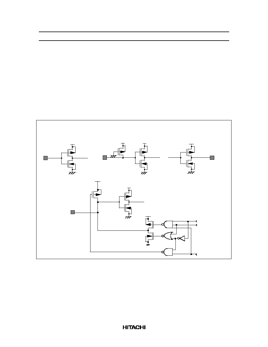
HD66727
91
Electrical Characteristics Notes
1. All voltage values are referred to GND = 0V. If the LSI is used above the absolute maximum ratings, it
may become permanently damaged. Using the LSI within the given electrical characteristic is strongly
recommended to ensure normal operation. If these electrical characteristic are exceeded, the LSI may
malfunction or exhibit poor reliability.
2. V
CC
> V1
V2
V3
V4
V5 > V
EE
must be maintained.
3. For bare die products, specified at 75
∞
C.
4. For bare die products, specified by the common die shipment specification.
5. The following four circuits are I/O pin configurations except for liquid crystal display output (Figure
51).
Pins: SCL, ID1/CS*, ID0,
OSC1, OPOFF, IM,
EXM, TEST
Pins: KST7 to KST0, IRQ*
LED2 to LED0, PORT2 to PORT0
PMOS
NMOS
V
CC
GND
Pins: KIN3 to KIN0, RESET*
Pin: SDA
(Pull-up MOS)
NMOS
PMOS
V
CC
PMOS
V
CC
GND
PMOS
NMOS
V
CC
GND
NMOS
PMOS
V
CC
(Pull-up MOS)
V
CC
V
CC
PMOS
NMOS
(Tri-state output circuit)
Output data
Output enable
GND
PMOS
IM
(Input circuit)
Figure 51 I/O Pin Configurations
6. The TEST pin must be grounded and the ID1 and ID0, IM, EXM, and OPOFF pins must be grounded or
connected to V
CC
.
7. Corresponds to the high output for clock-synchronized serial interface.
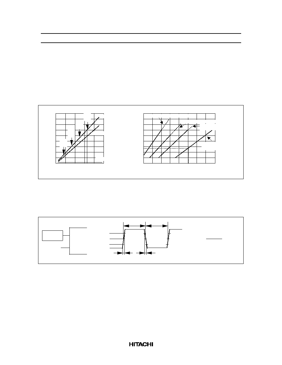
HD66727
92
8. Applies to resistor values (R
COM
) between power supply pins V
CC
, V1OUT, V4OUT, V5OUT and
common signal pins (COM1 to COM32, COMS1, and COMS2), and resistor values (R
SEG
) between
power supply pins V
CC
, V2OUT, V3OUT, V5OUT and segment signal pins (SEG1 to SEG60).
9. This excludes the current flowing through pull-up MOSs and output drive MOSs.
10. This excludes the current flowing through the input/output units. The input level must be fixed high or
low because through current increases if the CMOS input is left floating.
11. The following shows the relationship between the operation frequency (f
OSC
) and current consumption
(I
CC
) (Figure 52).
R-C oscillation frequencies: fosc (kHz)
40
30
20
10
0
Icc (
µ
A)
V
CC
= 3V
0 50 100 150 200 250
Display on (typ.)
Sleep mode (typ.)
Standby mode (typ.)
1/34
duty
1/26
duty
1/18
duty
1/10
duty
80
60
40
20
0
IEE (
µ
A)
V
CC
= 3V
3 4 5 6 7 8 9 10 11
LCD drive voltages: VLCD (V)
VREF-VREFP short-circuited
VREF left disconnected
VREF-VREFM
short-circuited
VREF = VREFP = VREFM
short-circuited
Figure 52 Relationship between the Operation Frequency and Current Consumption
12. Each COM and SEG output voltage is within
±
0.15V of the LCD voltage (V
CC
, V1, V2, V3, V4, V5)
when there is no load.
13. Applies to the external clock input (Figure 53).
Oscillator
OSC1
Open
OSC2
t
rcp
t
fcp
T
h
T
l
0.7V
CC
0.5V
CC
0.3V
CC
Duty =
T
h
+T
l
T
h
100%
X
Figure 53 External Clock Supply

HD66727
93
14. Applies to the internal oscillator operations using oscillation resistor Rf (Figure 54).
OSC1
OSC2
R
f
Since the oscillation frequency varies depending on the OSC1 and OSC2
pin capacitance, the wiring length to these pins should be minimized.
Referential data
200
150
100
50
0
100
200
400
R
f
(k
)
f
OSC
(kHz)
160
160
300
500
600
700
800
V
CC
= 5 V (typ.)
V
CC
= 3 V (typ.)
Figure 54 Internal Oscillation
15. Booster characteristics test circuits are shown in Figure 55.
( Triple boosting )
GND
V
CC
1
µ
F
1
µ
F
Vci
C1
C2
V5OUT2
V5OUT3
1
µ
F
( Double boosting )
GND
V
CC
1
µ
F
+
1
µ
F
Vci
C1
C2
V5OUT2
V5OUT3
+
V
EE
+
V
EE
+
+
Figure 55 Booster
HD66727
94
VUP2 = V
CC
≠ V5OUT2; VUP3 = V
CC
≠ V5OUT3
5.0
4.0
3.0
2.0
4
5
6
7
8
9
10
11
(i) Relation between the obtained voltage and input voltage
Vci (V)
VUP2 (V)
typ.
Vci = V
CC
, fcp =160 kHz, Ta = 25
∞
C
5.0
4.0
3.0
2.0
6
7
8
9
10
11
12
13
14
15
typ.
Vci = V
CC
, fcp =160 kHz, Ta = 25
∞
C
VUP3 (V)
Vci (V)
Vci = V
CC
= 4.5 V, Rf = 180 k
, Io = 0.1 mA
(ii) Relation between the obtained voltage and temperature
Double boosting
Triple boosting
Double boosting
Triple boosting
Ta (
∞
C)
VUP2 (V)
100
60
20
0
≠20
≠60
7.5
8.0
8.5
9.0
9.5
typ.
Ta (
∞
C)
VUP3 (V)
100
60
20
0
≠20
≠60
6.5
7.0
7.5
8.0
8.5
typ.
(iii) Relation between the obtained voltage and capacitance
Vci = V
CC
= 4.5 V, Rf = 180 k
, Io = 0.1 mA
Vci = V
CC
= 2.7 V, Rf = 150 k
, Io = 0.1 mA
1.5
1.0
0.5
6.0
6.5
7.0
7.5
8.0
min.
typ.
C (
µ
F)
VUP3 (V)
Double boosting
Triple boosting
C (
µ
F)
VUP2 (V)
1.5
1.0
0.5
7.0
7.5
8.0
8.5
9.0
typ.
Referential data
Vci = V
CC
= 2.7 V, Rf = 150 k
, Io = 0.1 mA
Figure 55 Booster (cont)

HD66727
95
Vci = V
CC
= 4.5 V, Rf = 180 k
, Ta = 25
∞
C
Vci = V
CC
= 2.7 V, Rf = 150 k
, Ta = 25
∞
C
1.5
2.0
0.5
1.0
0.0
2.0
3.0
4.0
5.0
7.0
6.0
8.0
typ.
VUP3 (V)
Double boosting
Triple boosting
VUP2 (V)
1.5
1.0
2.0
0.5
0.0
7.0
6.0
7.5
6.5
8.0
8.5
9.0
I
O
(mA)
I
O
(mA)
typ.
Load Circuits
AC Characteristics Test Load Circuits
Data bus : SDA
Test Point
50 pF
Figure 56 Load Circuit

HD66727
96
Timing Characteristics
Clock-Synchronized Serial Interface Timing
CS*
SCL
SDA
t
CSU
t
SCH
VIL
t
SISU
t
scr
VIH
VIL
VIH
VIL
VIH
VIL
t
CH
VIH
VIL
VIH
VIL
t
CWL
t
scf
t
SIH
VIL
t
SCYC
Valid data
VIH
Start : S
End : P
Valid data
Figure 57 Clock-Synchronized Serial Interface Input Timing
CS*
SCL
SDA
t
CSU
t
SCH
VIL
t
SOD
t
scr
VIH
VIL
VIH
VIL
VIH
VIL
t
CH
VOH1
VOH1
VOH1
VOL1
t
CWL
t
scf
VIL
t
SCYC
Output data
VIH
Start : S
End : P
Output data
VIL
VIH
t
SOH
Figure 58 Clock-Synchronized Serial Interface Output Timing

HD66727
97
I
2
C Bus Interface Timing
Stop : P
SDA
SCL
VIL
VIH
VIL
VIH
VIL
VIL
VIH
VIH
VIH
VIL
VIH
VIL
VIH
t
BUP
t
STAH
t
SCLH
t
SCLL
t
sf
t
sr
t
SCL
VIH
VIL
t
SDAH
t
STAS
t
STOPS
t
SDAS
Stop : P
VIH
Start :S
Restart : Sr
Figure 59 I
2
C Bus Interface Timing
Reset Timing
RESET*
VIL
VIL
t
RES
Figure 60 Reset Timing