 | –≠–ª–µ–∫—Ç—Ä–æ–Ω–Ω—ã–π –∫–æ–º–ø–æ–Ω–µ–Ω—Ç: HD74AC240 | –°–∫–∞—á–∞—Ç—å:  PDF PDF  ZIP ZIP |
HD74AC240/HD74ACT240
Octal Buffer/Line Driver with 3-State Output
Description
The HD74AC240/HD74ACT240 is an octal buffer and line driver designed to be employed as a memory
address driver, clock driver and bus oriented transmitter or receiver which provides improved PC board
density.
Features
∑
3-State Outputs Drive Bus Lines or Buffer Memory Address Registers
∑
Outputs Source/Sink 24 mA
∑
HD74ACT240 has TTL-Compatible Inputs
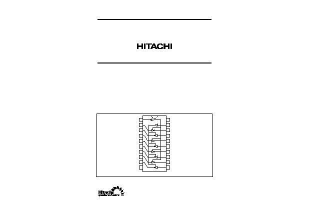
Pin Arrangement
1
2
3
4
5
6
7
8
9
10
11
12
13
14
15
16
17
18
19
20
GND
OE
1
V
CC
OE
2
(Top view)
HD74AC240/HD74ACT240
2
Truth Tables
Inputs
OE
1
D
Outputs (Pins 12, 14, 16, 18)
L
L
H
L
H
L
H
X
Z
Inputs
OE
2
D
Outputs (Pins 3, 5, 7, 9)
L
L
H
L
H
L
H
X
Z
H :
High Voltage Level
L
:
Low Voltage Level
X :
Immaterial
Z
:
High Impedance
DC Characteristics (unless otherwise specified)
Item
Symbol
Max
Unit
Condition
Maximum quiescent supply current
I
CC
80
µ
A
V
IN
= V
CC
or ground, V
CC
= 5.5 V,
Ta = Worst case
Maximum quiescent supply current
I
CC
8.0
µ
A
V
IN
= V
CC
or ground, V
CC
= 5.5 V,
Ta = 25
∞
C
Maximum additional I
CC
/input
(HD74ACT240)
I
CCT
1.5
mA
V
IN
= V
CC
≠ 2.1 V, V
CC
= 5.5 V,
Ta = Worst case

HD74AC240/HD74ACT240
3
AC Characteristics: HD74AC240
Ta = +25
∞
C
C
L
= 50 pF
Ta = ≠40
∞
C to +85
∞
C
C
L
= 50 pF
Item
Symbol
V
CC
(V)*
1
Min
Typ
Max
Min
Max
Unit
Propagation delay
t
PLH
3.3
1.0
6.0
8.0
1.0
9.0
ns
Data to output
5.0
1.0
4.5
6.5
1.0
7.0
Propagation delay
t
PHL
3.3
1.0
5.0
8.0
1.0
8.5
ns
Data to output
5.0
1.0
4.5
6.0
1.0
6.5
Output enable time
t
PZH
3.3
1.0
6.0
10.5
1.0
11.0
ns
5.0
1.0
5.0
7.0
1.0
8.0
Output enable time
t
PZL
3.3
1.0
7.0
10.0
1.0
11.0
ns
5.0
1.0
5.5
8.0
1.0
8.5
Output disable time
t
PHZ
3.3
1.0
7.0
10.0
1.0
10.5
ns
5.0
1.0
6.5
9.0
1.0
9.5
Output disable time
t
PLZ
3.3
1.0
7.5
10.5
1.0
11.5
ns
5.0
1.0
6.5
9.0
1.0
9.5
Note:
1. Voltage Range 3.3 is 3.3 V
±
0.3 V
Voltage Range 5.0 is 5.0 V
±
0.5 V
AC Characteristics: HD74ACT240
Ta = +25
∞
C
C
L
= 50 pF
Ta = ≠40
∞
C to +85
∞
C
C
L
= 50 pF
Item
Symbol
V
CC
(V)*
1
Min
Typ
Max
Min
Max
Unit
Propagation delay
Data to output
t
PLH
5.0
1.0
6.0
8.5
1.0
9.5
ns
Propagation delay
Data to output
t
PHL
5.0
1.0
5.5
7.5
1.0
8.5
ns
Output enable time
t
PZH
5.0
1.0
7.0
8.5
1.0
9.5
ns
Output enable time
t
PZL
5.0
1.0
7.0
9.5
1.0
10.5
ns
Output disable time
t
PHZ
5.0
1.0
8.0
9.5
1.0
10.5
ns
Output disable time
t
PLZ
5.0
1.0
6.5
10.0
1.0
10.5
ns
Note:
1. Voltage Range 5.0 is 5.0 V
±
0.5 V
HD74AC240/HD74ACT240
4
Capacitance
Item
Symbol
Typ
Unit
Condition
Input capacitance
C
IN
4.5
pF
V
CC
= 5.5 V
Power dissipation capacitance
C
PD
45.0
pF
V
CC
= 5.0 V

Hitachi Code
JEDEC
EIAJ
Weight (reference value)
DP-20N
--
Conforms
1.26 g
Unit: mm
0.51 Min
2.54 Min
5.08 Max
7.62
0.25
+ 0.11
≠ 0.05
2.54
±
0.25
0.48
±
0.10
24.50
25.40 Max
0.89
1.30
6.30
7.00 Max
1
10
11
20
0
∞
≠ 15
∞
1.27 Max