HD74AC245/HD74ACT245
Octal Bidirectional Transceiver with 3-State Input/Output
Description
The HD74AC245/HD74ACT245 contains eight non-inverting bidirectional buffers with 3-state outputs and
is intended for bus-oriented applications. Current sinking capability is 24 mA at both the A and B ports.
The Transmit/Receive (T/
R) input determines the direction of data flow through the bidirectional
transceiver. Transmit (active-High) enables data from A ports to B ports; Receive (active-Low) enables
data from B ports to A ports. The Output Enable input, when High, disables, both A and B ports by placing
them in a High Z condition.
Features
∑
Noninverting Buffers
∑
Bidirectional Data Path
∑
A and B Outputs Source/Sink 24 mA
∑
HD74ACT245 has TTL-Compatible Inputs
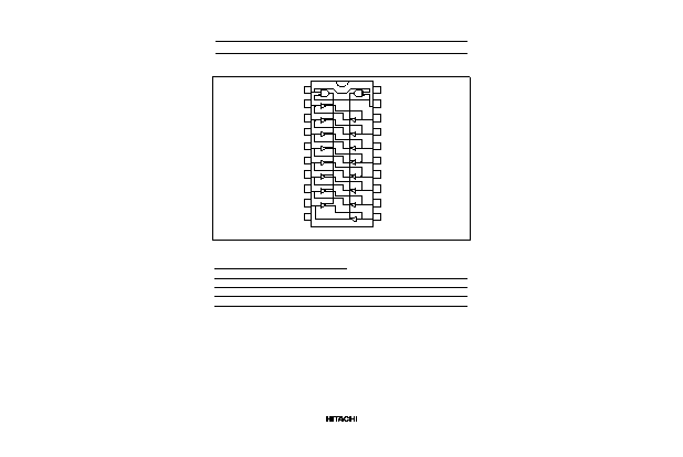
Pin Names
OE
Output Enable Input
T/
R
Transmit/Receive Input
A
0
to A
7
Side A 3-State Inputs or 3-State Outputs
B
0
to B
7
Side B 3-State Inputs or 3-State Outputs

HD74AC245/HD74ACT245
3
DC Characteristics (unless otherwise specified)
Item
Symbol
Max
Unit
Condition
Maximum quiescent supply current
I
CC
80
µ
A
V
IN
= V
CC
or ground, V
CC
= 5.5 V,
Ta = Worst case
Maximum quiescent supply current
I
CC
8.0
µ
A
V
IN
= V
CC
or ground, V
CC
= 5.5 V,
Ta = 25
∞
C
Maximum additional I
CC
/input
(HD74ACT245)
I
CCT
1.5
mA
V
IN
= V
CC
≠ 2.1 V, V
CC
= 5.5 V,
Ta = Worst case
AC Characteristics: HD74AC245
Ta = +25
∞
C
C
L
= 50 pF
Ta = ≠40
∞
C to +85
∞
C
C
L
= 50 pF
Item
Symbol
V
CC
(V)*
1
Min
Typ
Max
Min
Max
Unit
Propagation delay
t
PLH
3.3
1.0
5.0
8.5
1.0
9.0
ns
Data to output
5.0
1.0
3.5
6.5
1.0
7.0
Propagation delay
t
PHL
3.3
1.0
5.0
8.5
1.0
9.0
ns
Data to output
5.0
1.0
3.5
6.0
1.0
7.0
Output enable time
t
PZH
3.3
1.0
7.0
11.5
1.0
12.5
ns
5.0
1.0
5.0
8.5
1.0
9.0
Output enable time
t
PZL
3.3
1.0
7.5
12.0
1.0
13.5
ns
5.0
1.0
5.5
9.0
1.0
9.5
Output disable time
t
PHZ
3.3
1.0
6.5
12.0
1.0
12.5
ns
5.0
1.0
5.5
9.0
1.0
10.0
Output disable time
t
PLZ
3.3
1.0
7.0
11.5
1.0
13.0
ns
5.0
1.0
5.5
9.0
1.0
10.0
Note:
1. Voltage Range 3.3 is 3.3 V
±
0.3 V
Voltage Range 5.0 is 5.0 V
±
0.5 V

HD74AC245/HD74ACT245
4
AC Characteristics: HD74ACT245
Ta = +25
∞
C
C
L
= 50 pF
Ta = ≠40
∞
C to +85
∞
C
C
L
= 50 pF
Item
Symbol
V
CC
(V)*
1
Min
Typ
Max
Min
Max
Unit
Propagation delay
Data to output
t
PLH
5.0
1.0
4.0
7.5
1.0
8.0
ns
Propagation delay
Data to output
t
PHL
5.0
1.0
4.0
8.0
1.0
9.0
ns
Output enable time
t
PZH
5.0
1.0
5.0
10.0
1.0
11.0
ns
Output enable time
t
PZL
5.0
1.0
5.5
10.0
1.0
12.0
ns
Output disable time
t
PHZ
5.0
1.0
5.5
10.0
1.0
11.0
ns
Output disable time
t
PLZ
5.0
1.0
5.0
10.0
1.0
11.0
ns
Note:
1. Voltage Range 5.0 is 5.0 V
±
0.5 V
Capacitance
Item
Symbol
Typ
Unit
Condition
Input capacitance
C
IN
4.5
pF
V
CC
= 5.5 V
Input/output capacitance
C
I/O
15.0
pF
V
CC
= 5.5 V
Power dissipation capacitance
C
PD
45.0
pF
V
CC
= 5.0 V