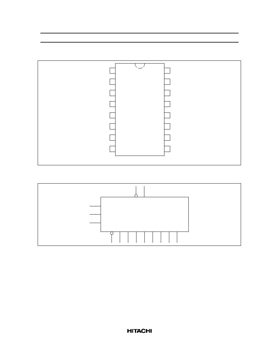
HD74AC259
8-bit Addressable Latch
Description
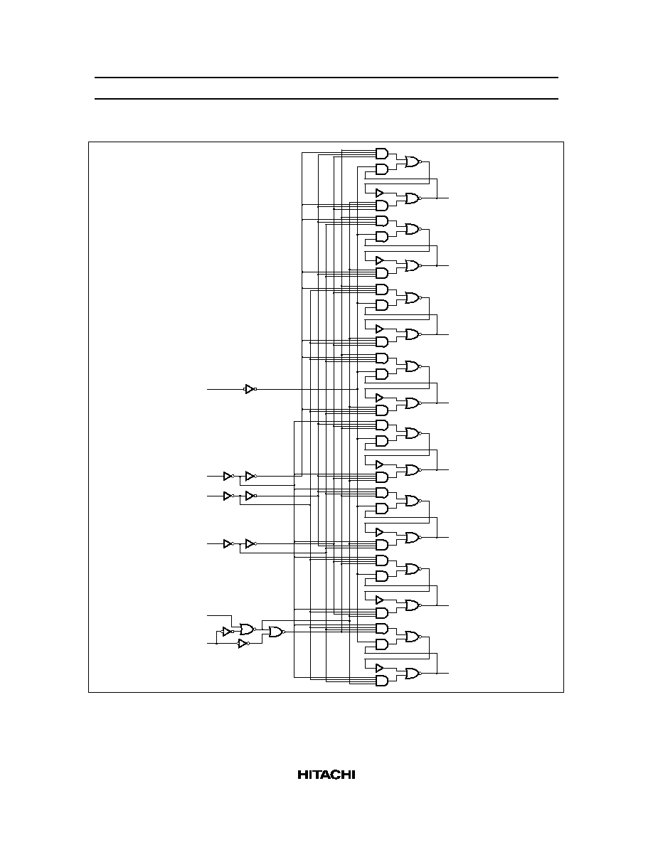
The HD74AC259 is a high-speed 8-bit addressable latch designed for general purpose storage applications
in digital systems. It is a multifunctional device capable or storing single line data in eight addressable
latches, and also a 1-of-8 decoder and demultiplexer with active HIGH outputs. The device also
incorporates an active LOW Common Clear for resetting all latches, as well as an active LOW Enable.
Features
∑
Serial-to-Parallel Conversion
∑
Eight Bits of Storage with Output of Each Bit Available
∑
Random (Addressable) Data Entry
∑
Active High Demultiplexing or Decoding Capability
∑
Easily Expandable
∑
Common Clear
∑
Outputs Source/Sink 24 mA
HD74AC259
4
Function Table
Inputs
Outputs
Operating Mode
MR E
D
A
0
A
1
A
2
Q
0
Q
1
Q
2
Q
3
Q
4
Q
5
Q
6
Q
7
Master reset
L
H
X
X
X
X
L
L
L
L
L
L
L
L
Demultiplex
L
L
d
L
L
L
Q = d L
L
L
L
L
L
L
(Active HIGH
L
L
d
H
L
L
L
Q = d L
L
L
L
L
L
Decoder when
L
L
d
L
H
L
L
L
Q = d L
L
L
L
L
D = H)
L
L
d
H
H
L
L
L
L
Q = d L
L
L
L
L
L
d
L
L
H
L
L
L
L
Q = d L
L
L
L
L
d
H
L
H
L
L
L
L
L
Q = d L
L
L
L
d
L
H
H
L
L
L
L
L
L
Q = d L
L
L
d
H
H
H
L
L
L
L
L
L
L
Q = d
Store (Do nothing)
H
H
X
X
X
X
q
0
q
1
q
2
q
3
q
4
q
5
q
6
q
7
Addressable latch
H
L
d
L
L
L
Q = d q
1
q
2
q
3
q
4
q
5
q
6
q
7
H
L
d
H
L
L
q
0
Q = d q
2
q
3
q
4
q
5
q
6
q
7
H
L
d
L
H
L
q
0
q
1
Q = d q
3
q
4
q
5
q
6
q
7
H
L
d
H
H
L
q
0
q
1
q
2
Q = d q
4
q
5
q
6
q
7
H
L
d
L
L
H
q
0
q
1
q
2
q
3
Q = d q
5
q
6
q
7
H
L
d
H
L
H
q
0
q
1
q
2
q
3
q
4
Q = d q
6
q
7
H
L
d
L
H
H
q
0
q
1
q
2
q
3
q
4
q
5
Q = d q
7
H
L
d
H
H
H
q
0
q
1
q
2
q
3
q
4
q
5
q
6
Q = d
H :
High Voltage Level
L
:
Low Voltage Level
X :
Immaterial
d
:
High or Low data one setup time prior to the Low-to-High Enable transition.
q
:
Lower case letters indicate the state of the referenced output established during the last cycle in
which it was addressed or cleared.
DC Characteristics (unless otherwise specified)
Item
Symbol
Max
Unit
Condition
Maximum quiescent supply current
I
CC
80
µ
A
V
IN
= V
CC
or ground, V
CC
= 5.5 V,
Ta = Worst case
Maximum quiescent supply current
I
CC
8.0
µ
A
V
IN
= V
CC
or ground, V
CC
= 5.5 V,
Ta = 25
∞
C
HD74AC259
5
AC Characteristics: HD74AC259
Ta = +25
∞
C
C
L
= 50 pF
Ta = ≠40
∞
C to +85
∞
C
C
L
= 50 pF
Item
Symbol
V
CC
(V)*
1
Min
Typ
Max
Min
Max
Unit
Maximum clock
f
max
3.3
65
--
--
60
--
MHz
frequency
5.0
110
--
--
95
--
Propagation delay
t
PHL
3.3
1.0
8.5
14.5
1.0
16.5
ns
MR
to Q
n
5.0
1.0
6.5
9.0
1.0
10.5
Propagation delay
t
PLH
3.3
1.0
7.0
10.5
1.0
12.0
ns
D
n
to Q
n
5.0
1.0
5.5
7.5
1.0
8.5
Propagation delay
t
PHL
3.3
1.0
7.0
10.5
1.0
12.0
ns
D
n
to Q
n
5.0
1.0
5.5
7.5
1.0
8.5
Propagaion delay
t
PLH
3.3
1.0
11.5
18.5
1.0
21.5
ns
A
n
to Q
n
5.0
1.0
8.0
11.5
1.0
14.0
Propagation delay
t
PHL
3.3
1.0
11.5
18.5
1.0
21.0
ns
A
n
to Q
n
5.0
1.0
8.0
11.5
1.0
13.5
Propagation delay
t
PLH
3.3
1.0
9.0
15.0
1.0
17.0
ns
E
to Q
5.0
1.0
6.5
9.0
1.0
10.5
Propagation delay
t
PHL
3.3
1.0
9.0
14.0
1.0
16.0
ns
E
to Q
n
5.0
1.0
6.5
8.5
1.0
10.0
Note:
1. Voltage Range 3.3 is 3.3 V
±
0.3 V
Voltage Range 5.0 is 5.0 V
±
0.5 V