
HD74ACT161/HD74ACT163
Synchronous Presettable Binary Counter
Description
The HD74ACT161 and HD74ACT163 are high-speed synchronous modulo-16 binary counters. They are
synchronously presettable for application in programmable dividers and have two types of Count Enable
inputs plus a Terminal Count output for versatility in forming synchronous multistage counters. The
HD74ACT161 have an asynchronous Master Reset input that overrides all other inputs and forces the
outputs Low. The HD74ACT163 has a Synchronous Reset input that overrides counting and parallel
loading and allows the outputs to be simultaneously reset on the rising edge of the clock.
Features
∑
Synchronous Counting and Loading
∑
High-Speed Synchronous Expansion
∑
Typical Count Rate of 125 MHz
∑
Outputs Source/Sink 24 mA
∑
HD74ACT161 and HD74ACT163 have TTL-Compatible Inputs

HD74ACT161/HD74ACT163
3
Pin Names
CEP
Count Enable Parallel Input
CET
Count Enable Trickle Input
CP
Clock Pulse Input
MR (HD74ACT161)
Asynchronous Master Reset Input
SR (HD74ACT163/HD74ACT163)
Synchronous Reset Input
P
0
to P
3
Parallel Data Inputs
PE
Parallel Enable Input
Q
0
to Q
3
Flip-Flop Outputs
TC
Terminal Count Output
Functional Description
The HD74ACT161 and HD74ACT163 count in modulo-16 binary sequence. From state 15 (HHHH) they
increment to state 0 (LLLL). The clock inputs of all flip-flops are driven in parallel through a clock buffer.
Thus all changes of the Q outputs (except due to Master Reset of the HD74ACT161) occur as a reset of,
and synchronous with, the Low-to-High transition of the CP input signal. The circuits have four
fundamental modes of operation, in order of precedence: asynchronous reset (HD74ACT161),
synchronous reset (HD74ACT163), parallel load, countup and hold. Five control inputs ≠ Master Reste
(
MR, HD74ACT161), Synchronous Reset (SR, HD74ACT163), Parallel Enable (PE), Count Enable
Parallel (CEP) and Count Enable Trickle (CET) ≠ determine the mode of operation, as shown in the Mode
Select Table. A Low signal on
MR overrides all other inputs and asynchronously forces all outputs Low.
A Low signal on
SR overrides counting and parallel loading and allows all outputs to go Low on the next
rising edge of CP. A Low signal on
PE overrides counting and allows information on the Parallel Data
(Pn) inputs to be loaded into the flip-flops on the next rising edge of CP. With
PE and MR (HD74ACT161)
or
SR (HD74ACT163) High, CEP and CET permit counting when both are High. Conversely, a Low
signal on either CEP or CET inhibits counting.
The HD74ACT161 and HD74ACT163 use D-type edge-triggered flip-flops and changing the
SR, PE, CEP
and CET inputs when the CP is in either state does not cause errors, provided that the recommended setup
and hold times, with respect to the rising edge of CP, are observed. The Terminal Count (TC) output is
High when CET is High and counter is in state 15. To implement synchronous multistage counters, the TC
outputs can be used with the CEP and CET inputs in two different ways. The TC output is subject to
decoding spikes due to internal race conditions and is therefore not recommended for use as a clock or
asynchronous reset for flip-flops, counters or registers.
Logic Equations: Count Enable = CEP∑CET∑
PE
TC = Q
0
∑Q
1
∑Q
2
∑Q
3
∑CET
HD74ACT161/HD74ACT163
5
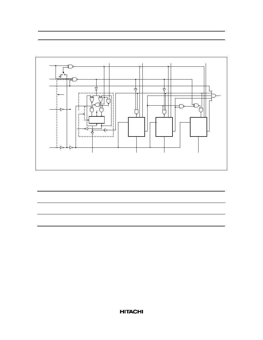
Block Diagram
PE
CEP
CET
CP
MR
'161
'163
SR
CP
'163
ONRY
'161
ONRY
DETAIL A
DETAIL A
DETAIL A
DETAIL A
Q
0
Q
0
C
D
O
O
CP
CP
D
D
'161
'163
P
0
P
1
P
2
P
3
TC
Q
3
Q
2
Q
1
Q
0
Please note that this diagram is provided only for the understanding of logic operations and should not be
used to estimate propagation delays.
DC Characteristics (unless otherwise specified)
Item
Symbol
Max
Unit
Condition
Maximum quiescent supply current
I
CC
80
µ
A
V
IN
= V
CC
or ground, V
CC
= 5.5 V,
Ta = Worst case
Maximum quiescent supply current
I
CC
8.0
µ
A
V
IN
= V
CC
or ground, V
CC
= 5.5 V,
Ta = 25
∞
C
Maximum additional I
CC
/input
(HD74ACT161/HD74ACT163)
I
CCT
1.5
mA
V
IN
= V
CC
≠ 2.1 V, V
CC
= 5.5 V,
Ta = Worst case

