HD74AC164/HD74ACT164
Serial-In, Parallel-Out Shift Register
Description
The HD74AC164/HD74ACT164 is a high-speed 8-bit serial-in/parallel-out shift register. Serial data is
entered through a 2-input AND gate synchronous with the Low-to-High transition of the clock. The device
features an asynchronous Master Reset which clears the register, setting all outputs Low independent of the
clock.
Features
∑
Outputs Source/Sink 24 mA
∑
HD74ACT164 has TTL-Compatible Inputs
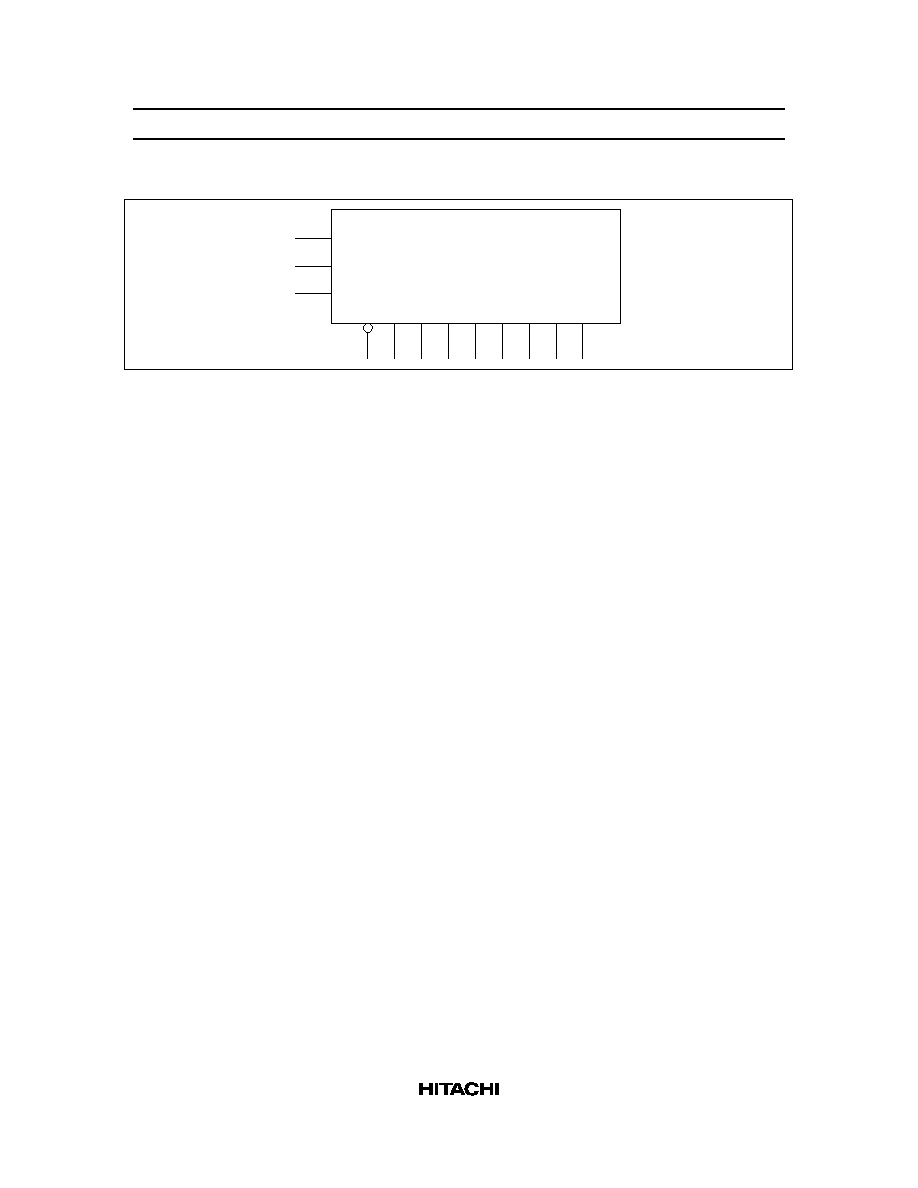
Pin Arrangement
1
2
3
4
5
6
7
14
13
12
11
10
9
8
A
B
Q
0
Q
1
Q
2
GND
Q
3
V
CC
Q
7
Q
6
Q
5
Q
4
MR
CP
(Top view)
HD74AC164/HD74ACT164
2
Logic Symbol
A
B
CP
MR Q
0
Q
1
Q
2
Q
3
Q
4
Q
5
Q
6
Q
7
Pin Names
A, B
Data Inputs
CP
Clock Pulse Input (Active Rising Edge)
MR
Master Reset Input (Active Low)
Q
0
to Q
7
Outputs
Functional Description
The HD74AC164/HD74ACT164 is an edge-triggered 8-bit shift register with serial data entry and an
output from each of the eight stages. Data is entered serially through one of two inputs (A or B); either of
these inputs can be used as an active High Enable for data entry through the other inputs. An unused input
must be tied High.
Each Low-to-High transition on the Clock (CP) input shifts data one place to the right and enters into Q
0
the logical AND of the two data inputs (A∑B) that existed before the rising clock edge. A Low level on the
Master Reset (
MR) input overrides all other inputs and clears the register asynchronously, forcing all Q
outputs Low.
HD74AC164/HD74ACT164
3
Mode Select Table
Inputs
Outputs
Operating Mode
MR
A
B
Q
0
Q
1
to Q
7
Reset (Clear)
L
X
X
L
L to L
Shift
H
L
L
L
q
0
to q
6
H
L
H
L
q
0
to q
6
H
H
L
L
q
0
to q
6
H
H
H
H
q
0
to q
6
H :
High Voltage Level
L
:
Low Voltage Level
X :
Immaterial
q
n
:
Lower case letters indicate the state of the referenced input or output one setup time prior to the
Low-to-High clock transition.
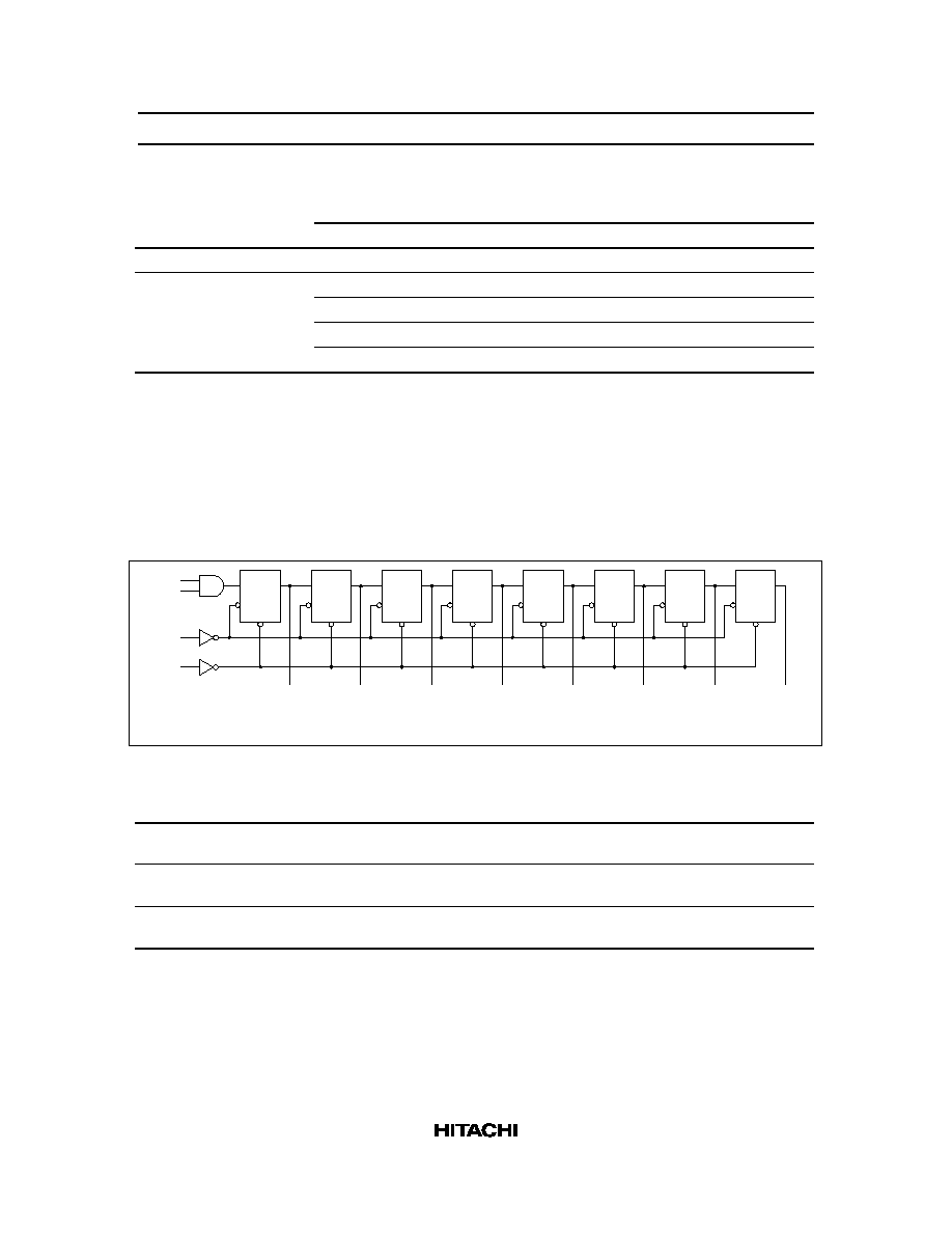
Logic Diagram
A
B
CP
MR
D
C
D
Q
0
Q
D
C
D
Q
1
Q
D
C
D
Q
2
Q
D
C
D
Q
3
Q
D
C
D
Q
4
Q
D
C
D
Q
5
Q
D
C
D
Q
6
Q
D
C
D
Q
7
Q
Please note that this diagram is provided only for the understanding of logic operations and should not be
used to estimate propagation delays.
DC Characteristics (unless otherwise specified)
Item
Symbol
Max
Unit
Condition
Maximum quiescent supply current
I
CC
80
µ
A
V
IN
= V
CC
or ground, V
CC
= 5.5 V,
Ta = Worst case
Maximum quiescent supply current
I
CC
8.0
µ
A
V
IN
= V
CC
or ground, V
CC
= 5.5 V,
Ta = 25
∞
C
Maximum additional I
CC
/input
(HD74ACT164)
I
CCT
1.5
mA
V
IN
= V
CC
≠ 2.1 V, V
CC
= 5.5 V,
Ta = Worst case

HD74AC164/HD74ACT164
4
AC Characteristics: HD74AC164
Ta = +25
∞
C
C
L
= 50 pF
Ta = ≠40
∞
C to +85
∞
C
C
L
= 50 pF
Item
Symbol
V
CC
(V)*
1
Min
Typ
Max
Min
Max
Unit
Maximum clock
f
max
3.3
125
--
--
100
--
MHz
frequency
5.0
150
--
--
125
--
Propagation delay
t
PLH
3.3
1.0
8.5
13.0
1.0
13.5
ns
CP to Q
n
5.0
1.0
6.5
10.0
1.0
10.5
Propagation delay
t
PHL
3.3
1.0
8.5
13.0
1.0
14.5
CP to Q
n
5.0
1.0
6.5
10.0
1.0
10.5
Propagation delay
t
PHL
3.3
1.0
9.5
16.0
1.0
18.0
MR
to Q
n
5.0
1.0
7.5
11.5
1.0
13.5
Note:
1. Voltage Range 3.3 is 3.3 V
±
0.3 V
Voltage Range 5.0 is 5.0 V
±
0.5 V
AC Operating Requirements: HD74AC164
Ta = +25
∞
C
C
L
= 50 pF
Ta = ≠40
∞
C
to +85
∞
C
C
L
= 50 pF
Item
Symbol
V
CC
(V)*
1
Typ
Guaranteed Minimum
Unit
Setup time A or B to CP
t
su
3.3
3.0
5.5
6.0
ns
5.0
2.0
4.6
4.5
Hold time CP to A or B
t
h
3.3
≠1.5
0.0
0.0
5.0
≠1.5
0.0
0.0
Pulse width CP or
MR
t
w
3.3
2.0
5.5
7.0
5.0
2.0
4.5
5.0
Recovery time
MR
or CP
t
rec
3.3
≠2.5
0.0
0.0
5.0
≠1.5
0.0
0.0
Note:
1. Voltage Range 3.3 is 3.3 V
±
0.3 V
Voltage Range 5.0 is 5.0 V
±
0.5 V
HD74AC164/HD74ACT164
5
AC Characteristics: HD74ACT164
Ta = +25
∞
C
C
L
= 50 pF
Ta = ≠40
∞
C to +85
∞
C
C
L
= 50 pF
Item
Symbol
V
CC
(V)*
1
Min
Typ
Max
Min
Max
Unit
Maximum clock
frequency
f
max
5.0
100
--
--
80
--
MHz
Propagation delay
CP to Q
n
t
PLH
5.0
1.0
9.0
11.5
1.0
12.5
ns
Propagation delay
CP to Q
n
t
PHL
5.0
1.0
9.0
11.5
1.0
12.5
Propagation delay
MR
to Q
n
t
PHL
5.0
1.0
9.5
13.0
1.0
14.5
Note:
1. Voltage Range 5.0 is 5.0 V
±
0.5 V
AC Operating Requirements: HD74ACT164
Ta = +25
∞
C
C
L
= 50 pF
Ta = ≠40
∞
C
to +85
∞
C
C
L
= 50 pF
Item
Symbol
V
CC
(V)*
1
Typ
Guaranteed Minimum
Unit
Setup time A or B to CP
t
su
5.0
2.5
7.0
8.0
ns
Hold time CP to A or B
t
h
5.0
0.0
1.5
1.5
Pulse width CP or
MR
t
w
5.0
4.5
7.0
8.0
Recovery time
MR
or CP
t
rec
5.0
0.0
2.0
2.0
Note:
1. Voltage Range 5.0 is 5.0 V
±
0.5 V
Capacitance
Item
Symbol
Typ
Unit
Condition
Input capacitance
C
IN
4.5
pF
V
CC
= 5.5 V
Power dissipation capacitance
C
PD
20.0
pF
V
CC
= 5.0 V