HD74AC182/HD74ACT182
Carry Lookhead Generator
Description
The HD74AC182/HD74ACT182 is a high-speed carry lookahead generator. It is generally used with the
HD74AC181 or HD74AC381 4-bit arithmetic logic unit to provide high-speed lookahead over word
lengths of more than four bits.
Features
∑
Outputs Source/Sink 24 mA
∑
HD74ACT182 has TTL-Compatible Inputs
Pin Arrangement
1
2
3
4
5
6
7
8
16
15
14
13
12
11
10
9
G
1
P
1
G
0
P
0
G
3
P
P
3
GND
V
CC
P
2
G
2
C
n
C
n+X
C
n+y
G
C
n+z
(Top view)
HD74AC182/HD74ACT182
2
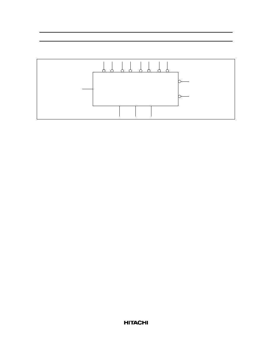
Logic Symbol
C
n
G
P
P
0
C
n+x
C
n+y
C
n+z
G
0
P
1
G
1
P
2
G
2
P
3
G
3
Pin Names
Cn
Carry Input
G
0
,
G
2
Carry Generate Inputs (Active Low)
G
1
Carry Generate Input (Active Low)
G
3
Carry Generate Input (Active Low)
P
0
,
P
1
Carry Propagate Inputs (Active Low)
P
2
Carry Propagate Input (Active Low)
P
3
Carry Propagate Input (Active Low)
C
n + x
to C
n + z
Carry Outputs
G
Carry Generate Output (Active Low)
P
Carry Propagate Output (Active Low)
HD74AC182/HD74ACT182
3
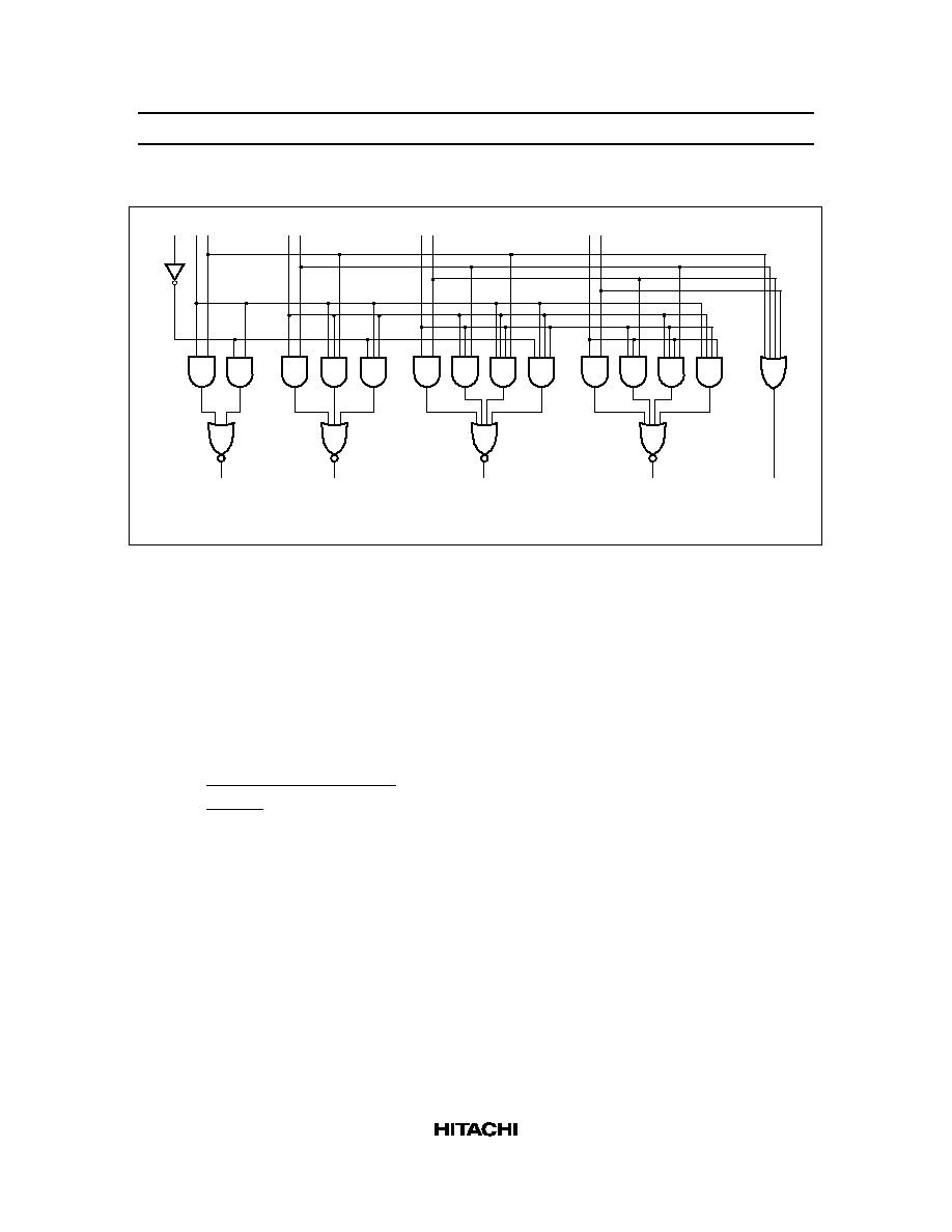
Logic Diagram
C
n
C
n+x
C
n+y
C
n+z
G
0
P
0
G
1
G
P
P
1
G
2
P
2
G
3
P
3
Please note that this diagram is provided only for the understanding of logic operations and should not be
used to estimate propagation delays.
Functional Description
The HD74AC182/HD74ACT182 carry lookahead generator accepts up to four pairs of Active Low Carry
Propagate (
P
0
to
P
3
) and Carry Generate (
G
0
to
G
3
) signals and an Active High Carry input (Cn) and
provides anticipated Active High carries (C
n + x
, C
n + y
, C
n + z
) across four groups of binary adders. The
HD74AC182/HD74ACT182 also has Active Low Carry Propagate (
P) and Carry Generate (G) outputs
which may be used for further level of lookahead. The logic equations provided at the outputs are:
C
n + x
= G
0
+ P
0
C
n
C
n + y
= G
1
+ P
1
G
0
+ P
1
P
0
C
n
C
n + z
= G
2
+ P
2
G
1
+ P
2
P
1
G
0
+ P
2
P
1
P
0
C
n
G
= G
3
+ P
3
G
2
+ P
3
P
2
G
1
+ P
3
P
2
P
1
G
0
P
= P
3
P
2
P
1
P
0
Also, the HD74AC182/HD74ACT182 can be used with binary ALUs in an active Low or active High input
operand mode. The connections (Figure a) to and from the ALU to the carry lookahead generator are
identical in both cases. Carries are rippled between lookahead blocks. The critical speed path follows the
circled numbers. There are several possible arrangements for the carry interconnects, but all achieve about
the same speed. A 28-bit ALU is formed by dropping the last HD74AC182/HD74ACT182.

HD74AC182/HD74ACT182
4
Truth Table
Inputs
Outputs
C
n
G
0
P
0
G
1
P
1
G
2
P
2
G
3
P
3
C
n + x
C
n + y
C
n + z
G
P
X
H
H
L
L
H
X
L
X
L
X
H
H
X
L
H
X
X
X
H
H
L
X
H
H
H
X
L
L
H
X
H
X
L
X
X
X
L
X
H
X
L
X
X
L
H
H
X
L
X
L
H
X
X
X
X
X
H
H
L
X
X
X
H
H
H
X
L
X
H
H
H
X
H
X
L
L
H
X
H
X
H
X
L
X
X
X
X
X
L
X
H
X
X
X
L
X
X
L
H
X
L
X
X
L
X
L
H
H
X
L
X
L
X
L
H
X
X
X
X
X
H
H
H
X
X
X
H
H
H
X
H
X
H
H
H
X
H
X
H
H
H
X
H
X
H
X
H
X
X
X
X
X
L
X
L
X
X
X
L
X
X
L
L
X
L
X
X
L
X
L
L
L
X
L
X
L
X
L
L
H
X
X
X
H
X
H
X
X
H
X
X
H
X
H
X
X
X
H
H
L
L
L
L
L
H :
High Voltage Level
L
:
Low Voltage Level
X :
Immaterial
HD74AC182/HD74ACT182
5
DC Characteristics (unless otherwise specified)
Item
Symbol
Max
Unit
Condition
Maximum quiescent supply current
I
CC
80
µ
A
V
IN
= V
CC
or ground, V
CC
= 5.5 V,
Ta = Worst case
Maximum quiescent supply current
I
CC
8.0
µ
A
V
IN
= V
CC
or ground, V
CC
= 5.5 V,
Ta = 25
∞
C
Maximum I
CC
/input (HD74ACT182)
I
CCT
1.5
mA
V
IN
= V
CC
≠ 2.1 V, V
CC
= 5.5 V,
Ta = Worst case
AC Characteristics: HD74AC182
Ta = +25
∞
C
C
L
= 50 pF
Ta = ≠40
∞
C to +85
∞
C
C
L
= 50 pF
Item
Symbol
V
CC
(V)*
1
Min
Typ
Max
Min
Max
Unit
Propagation delay
t
PLH
3.3
1.0
8.0
10.5
1.0
11.5
ns
P
n
to P
5.0
1.0
5.5
8.0
1.0
9.0
Propagation delay
t
PHL
3.3
1.0
8.0
10.5
1.0
11.5
ns
P
n
to P
5.0
1.0
5.5
8.0
1.0
9.0
Propagation delay
t
PLH
3.3
1.0
9.5
12.0
1.0
13.0
ns
C
n
to C
n + x, y, z
5.0
1.0
7.5
10.0
1.0
11.0
Propagation delay
t
PHL
3.3
1.0
9.0
12.0
1.0
13.0
ns
C
n
to C
n + x, y, z
5.0
1.0
7.0
10.0
1.0
11.0
Propagation delay
t
PLH
3.3
1.0
10.5
13.0
1.0
14.0
ns
P
n
or G
n
to C
n + x, y, z
5.0
1.0
8.0
10.5
1.0
11.5
Propagation delay
t
PHL
3.3
1.0
11.5
14.0
1.0
15.5
ns
P
n
or G
n
to C
n + x, y, z
5.0
1.0
9.0
11.5
1.0
12.5
Note:
1. Voltage Range 3.3 is 3.3 V
±
0.3 V
Voltage Range 5.0 is 5.0 V
±
0.5 V