Äîêóìåíòàöèÿ è îïèñàíèÿ www.docs.chipfind.ru
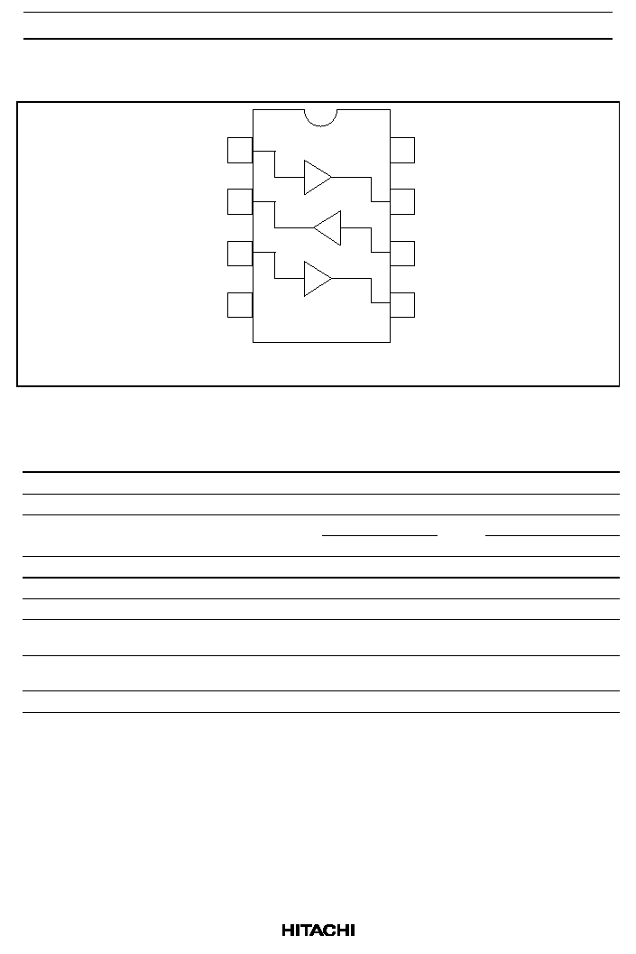
HD74ALVC2G34
Triple noninverter Buffers
ADE-205-635 (Z)
Rev. 0
July. 2001
Description
The HD74ALVC2G34 has triple noninverters in a 8 pin package. Low voltage and high speed operation is
suitable for the battery powered products (e.g., notebook computers), and the low power consumption
extends the battery life.
Features
· The basic gate function is lined up as hitachi uni logic series.
· Supplied on emboss taping for high speed automatic mounting.
· Supply voltage range : 1.2 to 3.6 V
Operating temperature range :
-40 to +85°C
· All inputs V
IH
(Max.) = 3.6 V (@V
CC
= 0 V to 3.6 V)
All outputs V
O
(Max.) = 3.6 V (@V
CC
= 0 V)
· Output current
±2 mA (@V
CC
= 1.2 V)
±4 mA (@V
CC
= 1.4 V to 1.6 V)
±6 mA (@V
CC
= 1.65 V to 1.95 V)
±18 mA (@V
CC
= 2.3 V to 2.7 V)
±24 mA (@V
CC
= 3.0 V to 3.6 V)
· Package type
Package type
Package code
Package suffix
Taping code
SSOP-8 pin
TTP-8DB
US
E (3,000 pcs / Reel)
HD74ALVC2G34
Rev.0, Jul. 2001, page 2 of 10
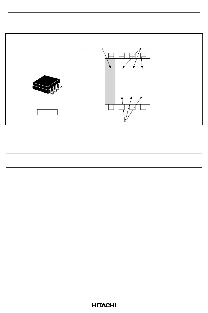
Outline and Article Indication
· HD74ALVC2G34
Lot No.
Y : Year code
(the last digit of year)
M : Month code
W : Week code
Y M W
A 3 4
Type No.
Index band
SSOP-8
Function Table
Input A
Output Y
H
H
L
L
H:
High level
L:
Low level
HD74ALVC2G34
Rev.0, Jul. 2001, page 3 of 10
Pin Arrangement
(Top view)
8
V
CC
1
7
1Y
6
3A
5
2Y
1A
2
3Y
3
2A
4
GND
Absolute Maximum Ratings
Item
Symbol
Ratings
Unit
Conditions
Supply voltage range
V
CC
-0.5 to 4.6
V
Input voltage range
*1
V
I
-0.5 to 4.6
V
Output voltage range
*1, 2
V
O
-0.5 to V
CC
+0.5
V
Output : H or L
-0.5 to 4.6
V
CC
: OFF
Input clamp current
I
IK
-50
mA
V
I
< 0
Output clamp current
I
OK
±50
mA
V
O
< 0 or V
O
> V
CC
Continuous output current
I
O
±50
mA
V
O
= 0 to V
CC
Continuous current through
V
CC
or GND
I
CC
or I
GND
±100
mA
Maximum power dissipation
at Ta = 25°C (in still air)
*3
P
T
200
mW
Storage temperature
Tstg
-65 to 150
°C
Notes:
The absolute maximum ratings are values which must not individually be exceeded, and
furthermore, no two of which may be realized at the same time.
1. The input and output voltage ratings may be exceeded if the input and output clamp-current
ratings are observed.
2. This value is limited to 4.6 V maximum.
3. The maximum package power dissipation was calculated using a junction temperature of 150°C.
HD74ALVC2G34
Rev.0, Jul. 2001, page 4 of 10
Recommended Operating Conditions
Item
Symbol
Min
Max
Unit
Conditions
Supply voltage range
V
CC
1.2
3.6
V
Input voltage range
V
I
0
3.6
V
Output voltage range
V
O
0
V
CC
V
Output current
I
OH
-2
mA
V
CC
= 1.2 V
-4
V
CC
= 1.4 V
-6
V
CC
= 1.65 V
-18
V
CC
= 2.3 V
-24
V
CC
= 3.0 V
I
OL
2
V
CC
= 1.2 V
4
V
CC
= 1.4 V
6
V
CC
= 1.65 V
18
V
CC
= 2.3 V
24
V
CC
= 3.0 V
Input transition rise or fall rate
t / v
0
20
ns / V
V
CC
= 1.2 to 2.7 V
0
10
V
CC
= 3.3
±0.3 V
Operating free-air temperature
Ta
-40
85
°C
Note:
Unused or floating inputs must be held high or low.

HD74ALVC2G34
Rev.0, Jul. 2001, page 5 of 10
Electrical Characteristics
(Ta =
-40 to 85°C)
Item
Symbol
V
CC
(V)
*
Min
Typ
Max
Unit
Test conditions
Input voltage
V
IH
1.2
V
CC
×0.75
V
1.4 to 1.6
V
CC
×0.7
1.65 to 1.95
V
CC
×0.7
2.3 to 2.7
1.7
3.0 to 3.6
2.0
V
IL
1.2
V
CC
×0.25
1.4 to 1.6
V
CC
×0.3
1.65 to 1.95
V
CC
×0.3
2.3 to 2.7
0.7
3.0 to 3.6
0.8
Output voltage
V
OH
Min to Max
V
CC
-0.2
V
I
OH
=
-100 µA
1.2
0.9
I
OH
=
-2 mA
1.4
1.1
I
OH
=
-4 mA
1.65
1.2
I
OH
=
-6 mA
2.3
1.7
I
OH
=
-18 mA
3.0
2.2
I
OH
=
-24 mA
V
OL
Min to Max
0.2
I
OL
= 100
µA
1.2
0.3
I
OL
= 2 mA
1.4
0.3
I
OL
= 4 mA
1.65
0.3
I
OL
= 6 mA
2.3
0.55
I
OL
= 18 mA
3.0
0.55
I
OL
= 24 mA
Input current
I
IN
3.6
±5
µA
V
IN
= 3.6 V or GND
Quiescent supply
current
I
CC
3.6
10
µA
V
IN
= V
CC
or GND,
I
O
= 0
Output leakage
current
I
OFF
0
5
µA
V
IN
or V
O
=
0 to 3.6 V
Input capacitance
C
IN
3.3
5.0
pF
V
IN
= V
CC
or GND
Note:
For conditions shown as Min or Max, use the appropriate values under recommended operating
conditions.