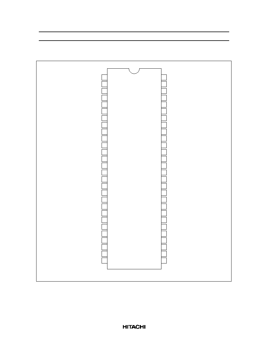
HD74ALVCH16820
3.3-V 10-bit Flip Flops with Dual Outputs
ADE-205-170B (Z)
3rd. Edition
December 1999
Description
The flip flops of the HD74ALVCH16820 are edge triggered D-type flip flops. On the positive transition of
the clock (CLK) input, the device provides true data at the Q outputs. A buffered output enable (
OE) input
can be used to place the ten outputs in either a normal logic state (high or low logic level) or a high
impedance state. In the high impedance state, the outputs neither load nor drive the bus lines significantly.
The high impedance state and increased drive provide the capability to drive bus lines without need for
interface or pullup components.
OE input does not affect the internal operation of the flip flops. Old data
can be retained or new data can be entered while the outputs are in the high impedance state. Active bus
hold circuitry is provided to hold unused or floating data inputs at a valid logic level.
Features
∑
V
CC
= 2.3 V to 3.6 V
∑
Typical V
OL
ground bounce < 0.8 V (@V
CC
= 3.3 V, Ta = 25
∞
C)
∑
Typical V
OH
undershoot > 2.0 V (@V
CC
= 3.3 V, Ta = 25
∞
C)
∑
High output current
±
24 mA (@V
CC
= 3.0 V)
∑
Bus hold on data inputs eliminates the need for external pullup / pulldown resistors

HD74ALVCH16820
4
Absolute Maximum Ratings
Item
Symbol
Ratings
Unit
Conditions
Supply voltage
V
CC
≠0.5 to 4.6
V
Input voltage
*1
V
I
≠0.5 to 4.6
V
Output voltage
*1, 2
V
O
≠0.5 to V
CC
+0.5
V
Input clamp current
I
IK
≠50
mA
V
I
< 0
Output clamp current
I
OK
±
50
mA
V
O
< 0 or V
O
> V
CC
Continuous output current
I
O
±
50
mA
V
O
= 0 to V
CC
V
CC
, GND current / pin
I
CC
or I
GND
±
100
mA
Maximum power dissipation
at Ta = 55
∞
C (in still air)
*3
P
T
1
W
TSSOP
Storage temperature
Tstg
≠65 to 150
∞
C
Notes:
Stresses beyond those listed under "absolute maximum ratings" may cause permanent damage
to the device. These are stress ratings only, and functional operation of the device at these or
any other conditions beyond those indicated under "recommended operating conditions" is not
implied. Exposure to absolute maximum rated conditions for extended periods may affect device
reliability.
1. The input and output negative voltage ratings may be exceeded if the input and output clamp
current ratings are observed.
2. This value is limited to 4.6 V maximum.
3. The maximum package power dissipation is calculated using a junction temperature of 150
∞
C
and a board trace length of 750 mils.
Recommended Operating Conditions
Item
Symbol
Min
Max
Unit
Conditions
Supply voltage
V
CC
2.3
3.6
V
Input voltage
V
I
0
V
CC
V
Output voltage
V
O
0
V
CC
V
High level output current
I
OH
--
≠12
mA
V
CC
= 2.3 V
--
≠12
V
CC
= 2.7 V
--
≠24
V
CC
= 3.0 V
Low level output current
I
OL
--
12
mA
V
CC
= 2.3 V
--
12
V
CC
= 2.7 V
--
24
V
CC
= 3.0 V
Input transition rise or fall rate
t /
v
0
10
ns / V
Operating temperature
Ta
≠40
85
∞
C
Note:
Unused control inputs must be held high or low to prevent them from floating.