Äîêóìåíòàöèÿ è îïèñàíèÿ www.docs.chipfind.ru

HD74CDC2510B
3.3-V Phase-lock Loop Clock Driver
ADE-205-219F (Z)
7th. Edition
October 1999
Description
The HD74CDC2510B is a high-performance, low-skew, low-jitter, phase-lock loop clock driver. It uses a
phase-lock loop (PLL) to precisely align, in both frequency and phase, the feedback (FBOUT) output to the
clock (CLK) input signal. It is specifically designed for use with synchronous DRAMs. The
HD74CDC2510B operates at 3.3 V V
CC
and is designed to drive up to five clock loads per output.
Bank of outputs provide ten low-skew, low-jitter copies of the input clock. Output signal duty cycles are
adjusted to 50 percent independent of the duty cycle at the input clock. Bank of outputs can be enabled or
disabled via the control (G) inputs. When the G inputs are high, the outputs switch in phase and frequency
with CLK; when the G inputs are low, the outputs are disabled to the logic-low state.
Unlike many products containing PLLs, the HD74CDC2510B does not require external RC networks. The
loop filter for the PLL is included on-chip, minimizing component count, board space, and cost.
Because it is based on PLL circuitry, HD74CDC2510B requires a stabilization time to achieve phase lock
of the feedback signal to the reference signal. This stabilization time is required, following power up and
application of a fixed-frequency, fixed-phase signal at CLK, as well as following any changes to the PLL
reference or feedback signals. The PLL can be bypassed for test purposes by strapping AV
CC
to ground.
Features
·
Meets "PC SDRAM registered DIMM design support document, Rev. 1.2"
·
Phase-lock loop clock distribution for synchronous DRAM applications
·
External feedback (FBIN) pin is used to synchronize the outputs to the clock input
·
No external RC network required
·
Support spread spectrum clock (SSC) synthesizers
Note:
Only by a change of a suffix (A to B) for standardization, there isn't any change of the product.
HD74CDC2510B
2
Function Table
I n p u t s
O u t p u t s
G
CLK
1Y (0:9)
FBOUT
X
L
L
L
L
H
L
H
H
H
H
H
H :
High level
L :
Low level
X :
Immaterial
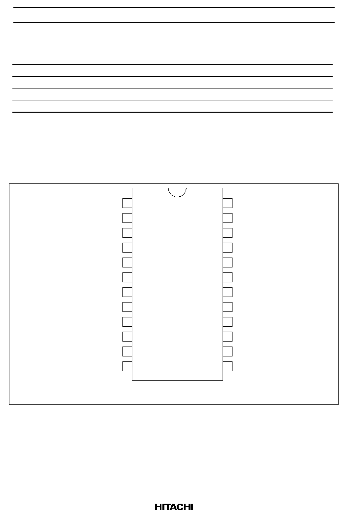
Pin Arrangement
(Top view)
15
16
17
18
19
20
21
22
23
24
V
CC
V
CC
AV
CC
V
CC
V
CC
1
2
3
4
5
6
7
8
9
10
11
12
AGND
1Y0
1Y1
1Y2
GND
GND
1Y3
1Y4
G
FBOUT
CLK
1Y9
1Y8
GND
GND
1Y7
1Y6
1Y5
13
14
FBIN
HD74CDC2510B
3
Absolute Maximum Ratings
I t e m
Symbol
R a t i n g s
U n i t
Conditions
Supply voltage
V
CC
0.5 to 4.6
V
Input voltage
*1
V
I
0.5 to 6.5
V
Output voltage
*1, 2
V
O
0.5 to V
CC
+0.5
V
Input clamp current
I
IK
50
mA
V
I
< 0
Output clamp current
I
OK
±
50
mA
V
O
< 0 or V
O
> V
CC
Continuous output current
I
O
±
50
mA
V
O
= 0 to V
CC
Supply current
I
CC
or I
GND
±
100
mA
Maximum power dissipation
at Ta = 55
°
C (in still air)
*3
P
T
0.7
W
Storage temperature
T
stg
65 to +150
°
C
Notes:
Stresses beyond those listed under "absolute maximum ratings" may cause permanent damage
to the device. These are stress ratings only, and functional operation of the device at these or
any other conditions beyond those indicated under "recommended operating conditions" is not
implied. Exposure to absolute maximum rated conditions for extended periods may affect
device reliability.
1. The input and output negative voltage ratings may be exceeded if the input and output clamp
current ratings are observed.
2. This value is limited to 4.6 V maximum.
3. The maximum package power dissipation is calculated using a junction temperature of 150
°
C and
a board trace length of 750 mils.
Recommended Operating Conditions
I t e m
Symbol Min
T y p
M a x
U n i t
Conditions
Supply voltage
V
CC
3.0
--
3.6
V
Input voltage
V
IH
2.0
--
--
V
V
IL
--
--
0.8
V
I
0
--
V
CC
Output current
I
O H
--
--
12
mA
I
O L
--
--
12
Operating temperature
T
a
0
--
85
°
C
Note: Unused inputs must be held high or low to prevent them from floating.
HD74CDC2510B
4
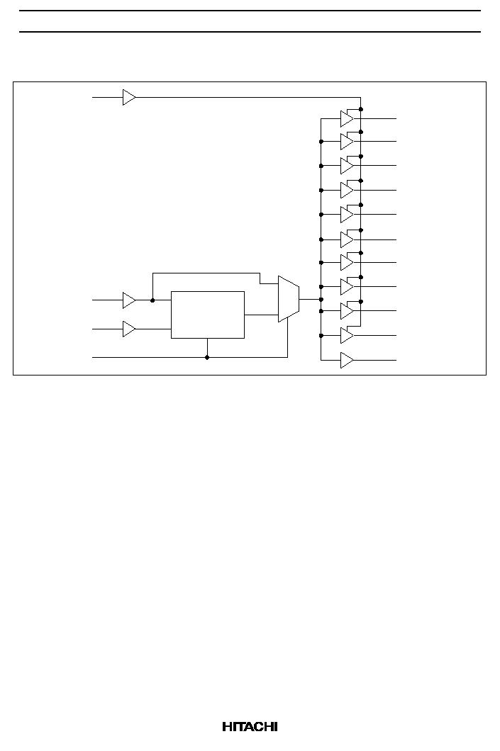
Logic Diagram
PLL
24
CLK
13
FBIN
AV
23
CC
1Y5
15
1Y6
16
11
G
1Y0
3
1Y1
4
1Y2
5
1Y3
8
1Y4
9
1Y7
17
1Y8
20
1Y9
21
FBOUT
12
HD74CDC2510B
5
Pin Function
Pin name
N o .
T y p e
Description
CLK
24
I
Clock input. CLK provides the clock signal to be distributed by the
HD74CDC2510B clock driver. CLK is used to provide the
reference signal to the integrated PLL that generates the clock
output signals. CLK must have a fixed frequency and fixed phase
for the PLL to obtain phase lock. Once the circuit is powered up
and a valid CLK signal is applied, a stabilization time is required for
the PLL to phase lock the feedback signal to its reference signal.
FBIN
13
I
Feedback input. FBIN provides the feedback signal to the internal
PLL. FBIN must be hard-wired to FBOUT to complete the PLL. The
integrated PLL synchronizes CLK and FBIN so that there is
nominally zero phase error between CLK and FBIN.
G
11
I
Output bank enable. G is the output enable for outputs 1Y(0:9).
When G is low, outputs 1Y(0:9)are disabled to a logic-low state.
When G is high, all outputs 1Y(0:9) are enabled and switch at the
same frequency as CLK.
FBOUT
12
O
Feedback output. FBOUT is dedicated for external feedback. It
switches at the same frequency as CLK. When externally wired to
FBIN, FBOUT completes the feedback loop of the PLL.
1Y(0:9)
3, 4, 5, 8, 9,
15, 16, 17,
20, 21
O
Clock outputs. These outputs provide low-skew copies of CLK.
Output bank 1Y(0:9) is enabled via the G input. These outputs can
be disabled to a logic low state by deasserting the G control input.
AV
CC
23
Power
Analog power supply. AV
CC
provides the power reference for the
analog circuitry. In addition, AV
CC
can be used to bypass the PLL
for test purposes. When AV
CC
is strapped to ground, PLL is
bypassed and CLK is buffered directly to the device outputs.
AGND
1
Ground Analog ground. AGND provides the ground reference for the
analog circuitry.
V
CC
2, 10, 14, 22 Power
Power supply
GND
6, 7, 18,19
Ground Ground