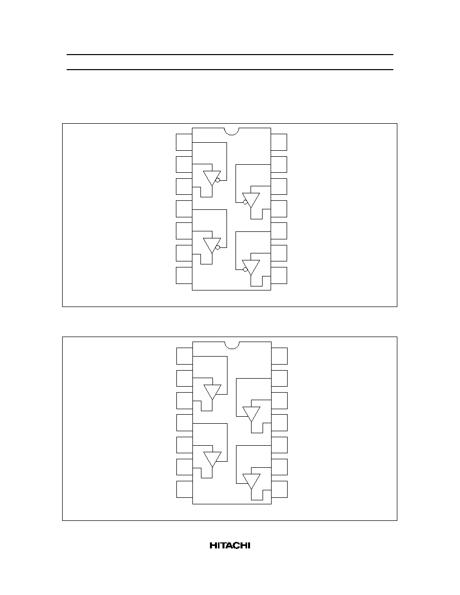
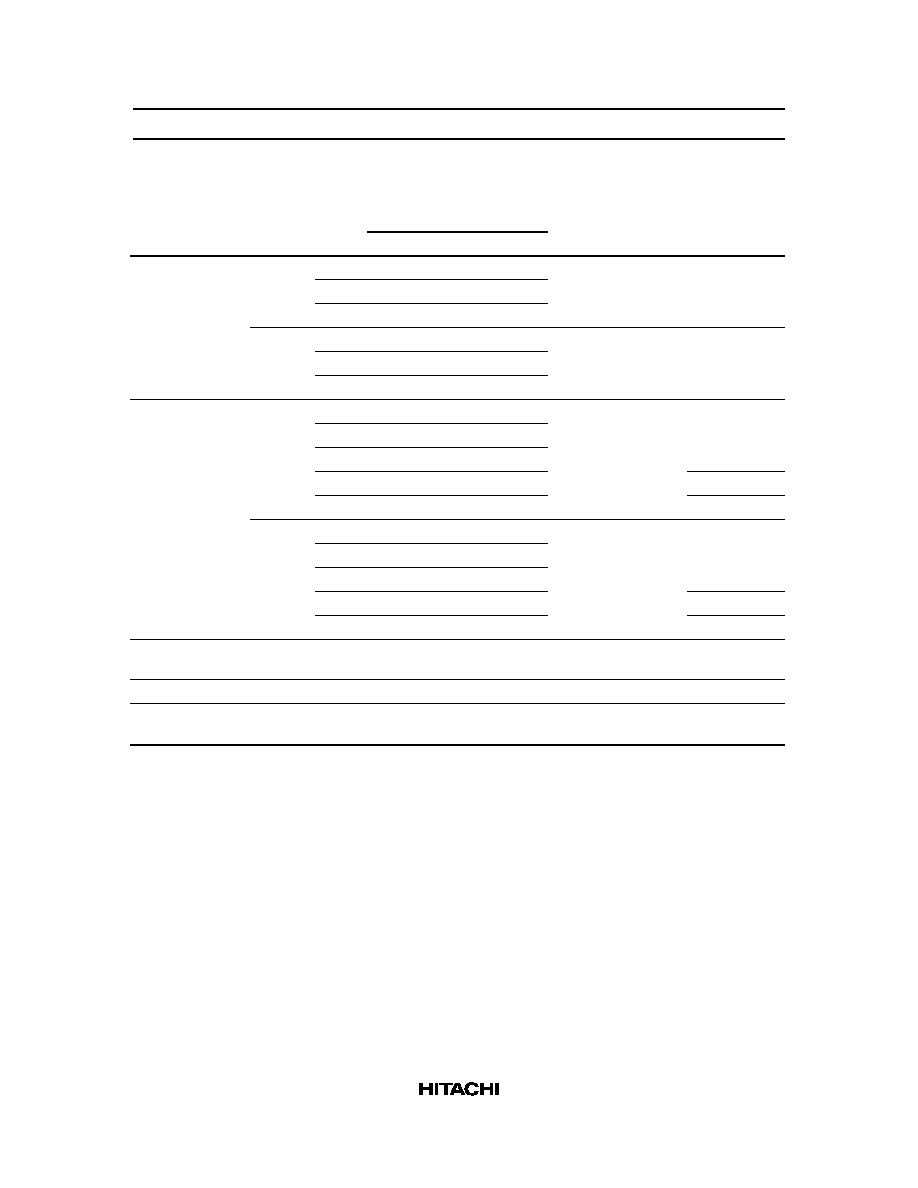
ChipFind - документация

Электронный компонент: HD74HC126

Скачать:  PDF   ZIP
HD74HC125/HD74HC126
Quad. Bus Buffer Gates (with 3-state outputs)
Description
The HD74HC125, HD74HC126 require the 3-state control input C to be taken high to put the output into
the high impedance condition, whereas the HD74HC125, HD74HC126 requires the control input to be low
to put the output into high impedance.
Features
High Speed Operation: t
pd
= 8 ns typ (C
L
= 50 pF)
High Output Current: Fanout of 15 LSTTL Loads
Wide Operating Voltage: V
CC
= 2 to 6 V
Low Input Current: 1 A max
Low Quiescent Supply Current: I
CC
(static) = 4 A max (Ta = 25C)
Function Table
Inputs
C
Output Y
HC125
HC126
A
HC125
HC126
H
L
X
Z
Z
L
H
L
L
L
L
H
H
H
H
X :
Irrelevent
Z
:
Off (high-impedance) state of a 3-state output.
HD74HC125/HD74HC126
2
Pin Arrangement
HD74HC125
1
(Top view)
2
3
4
5
6
7
1C
1A
1Y
2C
2A
2Y
GND
V
CC
4C
4A
4Y
3C
3A
3Y
14
13
12
11
10
9
8
HD74HC126
1
(Top view)
2
3
4
5
6
7
1C
1A
1Y
2C
2A
2Y
GND
V
CC
4C
4A
4Y
3C
3A
3Y
14
13
12
11
10
9
8
HD74HC125/HD74HC126
3
Absolute Maximum Ratings
Item
Symbol
Rating
Unit
Supply voltage range
V
CC
0.5 to +7.0
V
Input voltage
V
IN
0.5 to V
CC
+ 0.5
V
Output voltage
V
OUT
0.5 to V
CC
+ 0.5
V
Output current
I
OUT
35
mA
DC current drain per V
CC
, GND
I
CC
, I
GND
75
mA
DC input diode current
I
IK
20
mA
DC output diode current
I
OK
20
mA
Power dissipation per package
P
T
500
mW
Storage temperautre
Tstg
65 to +150
C
HD74HC125/HD74HC126
4
DC Characteristics
Ta = 25
C
Ta = 40 to
+85
C
Item
Symbol
V
CC
(V) Min Typ Max Min
Max
Unit
Test Conditions
Input voltage
V
IH
2.0
1.5
--
--
1.5
--
V
4.5
3.15 --
--
3.15
--
6.0
4.2
--
--
4.2
--
V
IL
2.0
--
--
0.5
--
0.5
V
4.5
--
--
1.35 --
1.35
6.0
--
--
1.8
--
1.8
Output voltage
V
OH
2.0
1.9
2.0
--
1.9
--
V
Vin = V
IH
or V
IL
I
OH
= 20
A
4.5
4.4
4.5
--
4.4
--
6.0
5.9
6.0
--
5.9
--
4.5
4.18 --
--
4.13
--
I
OH
= 6 mA
6.0
5.68 --
--
5.63
--
I
OH
= 7.8 mA
V
OL
2.0
--
0.0
0.1
--
0.1
V
Vin = V
IH
or V
IL
I
OL
= 20
A
4.5
--
0.0
0.1
--
0.1
6.0
--
0.0
0.1
--
0.1
4.5
--
--
0.26 --
0.33
I
OL
= 6 mA
6.0
--
--
0.26 --
0.33
I
OL
= 7.8 mA
Off-state output
current
I
OZ
6.0
--
--
0.5 --
5.0
A
Vin = V
IH
or V
IL
,
Vout = V
CC
or GND
Input current
Iin
6.0
--
--
0.1 --
1.0
A
Vin = V
CC
or GND
Quiescent supply
current
I
CC
6.0
--
--
4.0
--
40
A
Vin = V
CC
or GND, Iout = 0
A
HD74HC125/HD74HC126
5
AC Characteristics (C
L
= 50 pF, Input t
r
= t
f
= 6 ns)
Ta = 25
C
Ta = 40 to
+85
C
Item
Symbol
V
CC
(V) Min Typ Max Min
Max
Unit
Test Conditions
Propagation delay t
PLH
2.0
--
--
100 --
125
ns
time
t
PHL
4.5
--
8
20
--
25
6.0
--
--
17
--
21
Output enable
t
ZH
2.0
--
--
150 --
190
ns
time
t
ZL
4.5
--
9
30
--
38
6.0
--
--
26
--
33
Output disable
t
HZ
2.0
--
--
150 --
190
ns
time
t
LZ
4.5
--
14
30
--
38
6.0
--
--
26
--
33
Output rise/fall
t
TLH
2.0
--
--
60
--
75
ns
time
t
THL
4.5
--
4
12
--
15
6.0
--
--
10
--
13
Input capacitance
Cin
--
--
5
10
--
10
pF