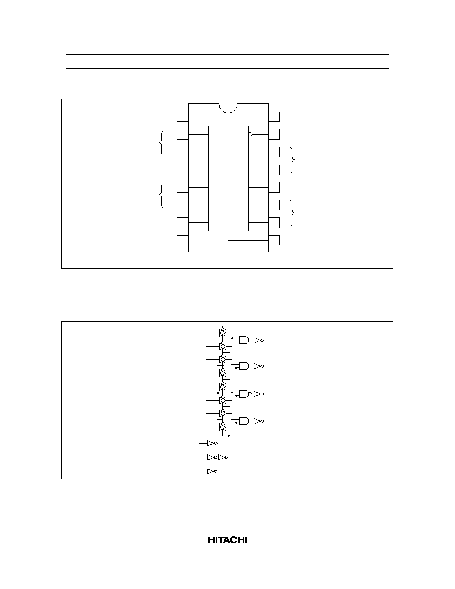
ChipFind - документация

Электронный компонент: HD74HC157

Скачать:  PDF   ZIP
HD74HC157/HD74HC158
Quad. 2-to-1-line Data Selectors/Multiplexers
(with noninverted outputs)
Quad. 2-to-1-line Data Selectors/Multiplexers
(with inverted outputs)
Description
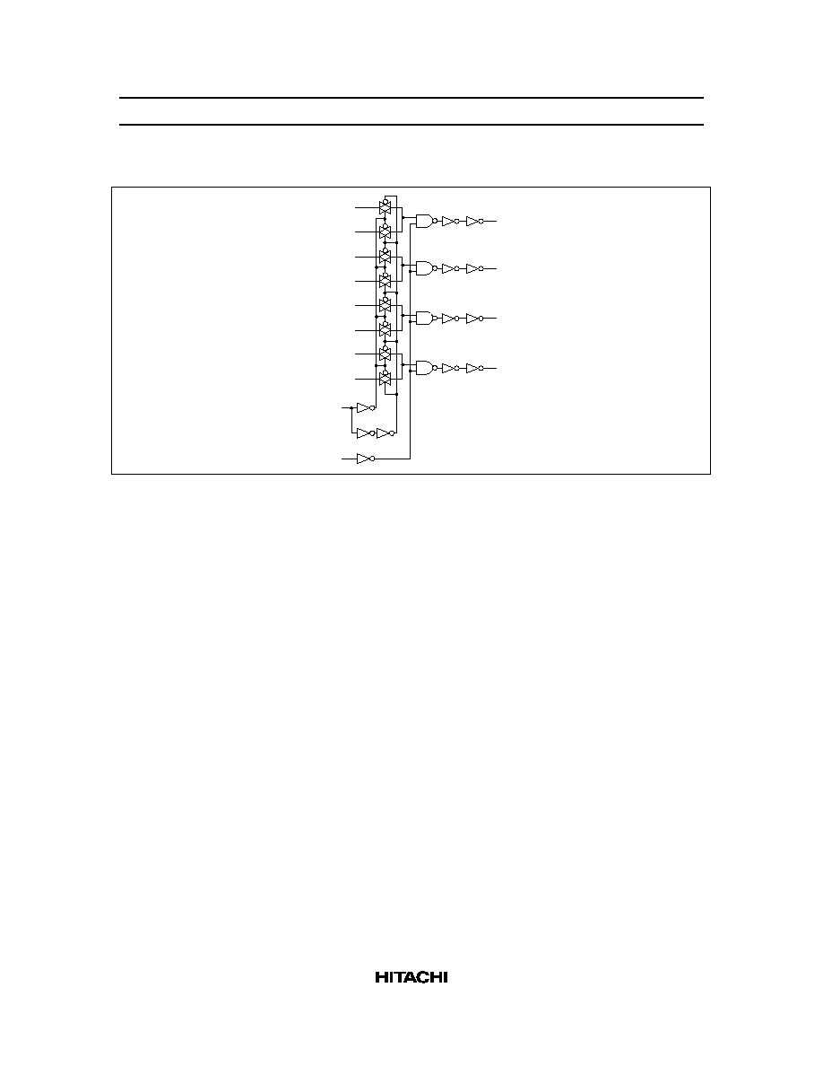
These devices each consist of four 2-input digital multiplexers with common select and strobe inputs. On
the HD74HC157, when the strobe input is at logical "L" the four outputs assume the values as selected
from the inputs. When the strobe input is at a logical "H" the outputs assume logical "L". The
HD74HC158 operates in the same manner, except that its outputs are inverted. Select decoding is done
internally resulting in a single select input only. If enabled, the select input determines whether the A or B
inputs get routed to their corresponding Y outputs.
Features
High Speed Operation: t
pd
(Data to Output) = 12 ns typ (C
L
= 50 pF)
High Output Current: Fanout of 10 LSTTL Loads
Wide Operating Voltage: V
CC
= 2 to 6 V
Low Input Current: 1 A max
Low Quiescent Supply Current: I
CC
(static) = 4 A max (Ta = 25C)
Function Table
Inputs
Output Y
Strobe
Select
A
B
HC157
HC158
H
X
X
X
L
H
L
L
L
X
L
H
L
L
H
X
H
L
L
H
X
L
L
H
L
H
X
H
H
L
HD74HC157/HD74HC158
2
Pin Arrangement
1
2
3
4
5
6
7
8
Select
1A
1B
1Y
2A
2B
2Y
GND
V
CC
Strobe
4A
4B
4Y
3A
3B
3Y
16
15
14
13
12
11
10
9
(Top view)
1A
2Y
1B
2A
2B
1Y
S
4A
4B
3A
3B
4Y
S
Inputs
Inputs
Output
Output
Output
Inputs
Inputs
Output
3Y
Logic Diagram
HD74HC157
1Y
2Y
3Y
4Y
1A
1B
2A
2B
3A
3B
4A
4B
Select
Strobe
HD74HC157/HD74HC158
3
HD74HC158
1Y
2Y
3Y
4Y
1A
1B
2A
2B
3A
3B
4A
4B
Select
Strobe
HD74HC157/HD74HC158
4
DC Characteristics
Ta = 25
C
Ta = 40 to
+85
C
Item
Symbol
V
CC
(V) Min Typ Max Min
Max
Unit
Test Conditions
Input voltage
V
IH
2.0
1.5
--
--
1.5
--
V
4.5
3.15 --
--
3.15
--
6.0
4.2
--
--
4.2
--
V
IL
2.0
--
--
0.5
--
0.5
V
4.5
--
--
1.35 --
1.35
6.0
--
--
1.8
--
1.8
Output voltage
V
OH
2.0
1.9
2.0
--
1.9
--
V
Vin = V
IH
or V
IL
I
OH
= 20
A
4.5
4.4
4.5
--
4.4
--
6.0
5.9
6.0
--
5.9
--
4.5
4.18 --
--
4.13
--
I
OH
= 4 mA
6.0
5.68 --
--
5.63
--
I
OH
= 5.2 mA
V
OL
2.0
--
0.0
0.1
--
0.1
V
Vin = V
IH
or V
IL
I
OL
= 20
A
4.5
--
0.0
0.1
--
0.1
6.0
--
0.0
0.1
--
0.1
4.5
--
--
0.26 --
0.33
I
OL
= 4 mA
6.0
--
--
0.26 --
0.33
I
OL
= 5.2 mA
Input current
Iin
6.0
--
--
0.1 --
1.0
A
Vin = V
CC
or GND
Quiescent supply
current
I
CC
6.0
--
--
4.0
--
40
A
Vin = V
CC
or GND, Iout = 0
A
HD74HC157/HD74HC158
5
AC Characteristics (C
L
= 50 pF, Input t
r
= t
f
= 6 ns)
Ta = 25
C
Ta = 40 to
+85
C
Item
Symbol
V
CC
(V) Min Typ Max Min
Max
Unit
Test Conditions
Propagation delay t
PLH
2.0
--
--
125 --
155
ns
Data to
HD74HC157 only
time
t
PHL
4.5
--
12
25
--
31
output
6.0
--
--
21
--
26
t
PLH
2.0
--
--
110 --
140
ns
HD74HC158 only
t
PHL
4.5
--
12
22
--
28
6.0
--
--
19
--
24
t
PHL
2.0
--
--
125 --
155
ns
Select to output
4.5
--
13
25
--
31
6.0
--
--
21
--
26
t
PLH
2.0
--
--
160 --
200
ns
4.5
--
17
32
--
40
6.0
--
--
27
--
34
t
PHL
2.0
--
--
160 --
200
ns
Strobe to output
4.5
--
12
32
--
40
6.0
--
--
27
--
34
t
PLH
2.0
--
--
160 --
200
ns
4.5
--
12
32
--
40
6.0
--
--
27
--
34
Output rise/fall
t
TLH
2.0
--
--
75
--
95
ns
time
t
THL
4.5
--
5
15
--
19
6.0
--
--
13
--
16
Input capacitance
Cin
--
--
5
10
--
10
pF