HD74HC242/HD74HC243
Quad. Bus Transceivers (with 3-state outputs)
Quad. Bus Transceivers (with noninverted 3-state outputs)
Description
The HD74HC242 is an inverting buffer and the HD74HC243 is a noninverting buffer. Each device has one
active high enable (GBA), and one active low enable (
GAB). GBA enables the A output and GAB enables
the B outputs. The device does not have schmitt trigger inputs.
Features
∑
High Speed Operation: t
pd
= 10 ns typ (C
L
= 50 pF)
∑
High Output Current: Fanout of 15 LSTTL Loads
∑
Wide Operating Voltage: V
CC
= 2 to 6 V
∑
Low Input Current: 1 µA max
∑
Low Quiescent Supply Current: I
CC
(static) = 4 µA max (Ta = 25∞C)
Function Table
HD74HC242
HC74HC243
Control inputs
Data Port Status
Data Port Status
G
AB
GBA
A
B
A
B
H
H
O
I
O
I
L
H
Z
Z
Z
Z
H
L
Z
Z
Z
Z
L
L
I
O
I
O
I
:
Input
O :
Output
O
:
Inverting Output
Z
:
Hight Impedance
HD74HC242/HD74HC243
3
Absolute Maximum Ratings
Item
Symbol
Rating
Unit
Supply voltage range
V
CC
≠0.5 to +7.0
V
Input voltage
V
IN
≠0.5 to V
CC
+ 0.5
V
Output voltage
V
OUT
≠0.5 to V
CC
+ 0.5
V
DC current drain per pin
I
OUT
±
35
mA
DC current drain per VCC, GND
I
CC
, I
GND
±
75
mA
DC input diode current
I
IK
±
20
mA
DC output diode current
I
OK
±
20
mA
Power Dissipation per package
P
T
500
mW
Storage temperature
Tstg
≠65 to +150
∞
C
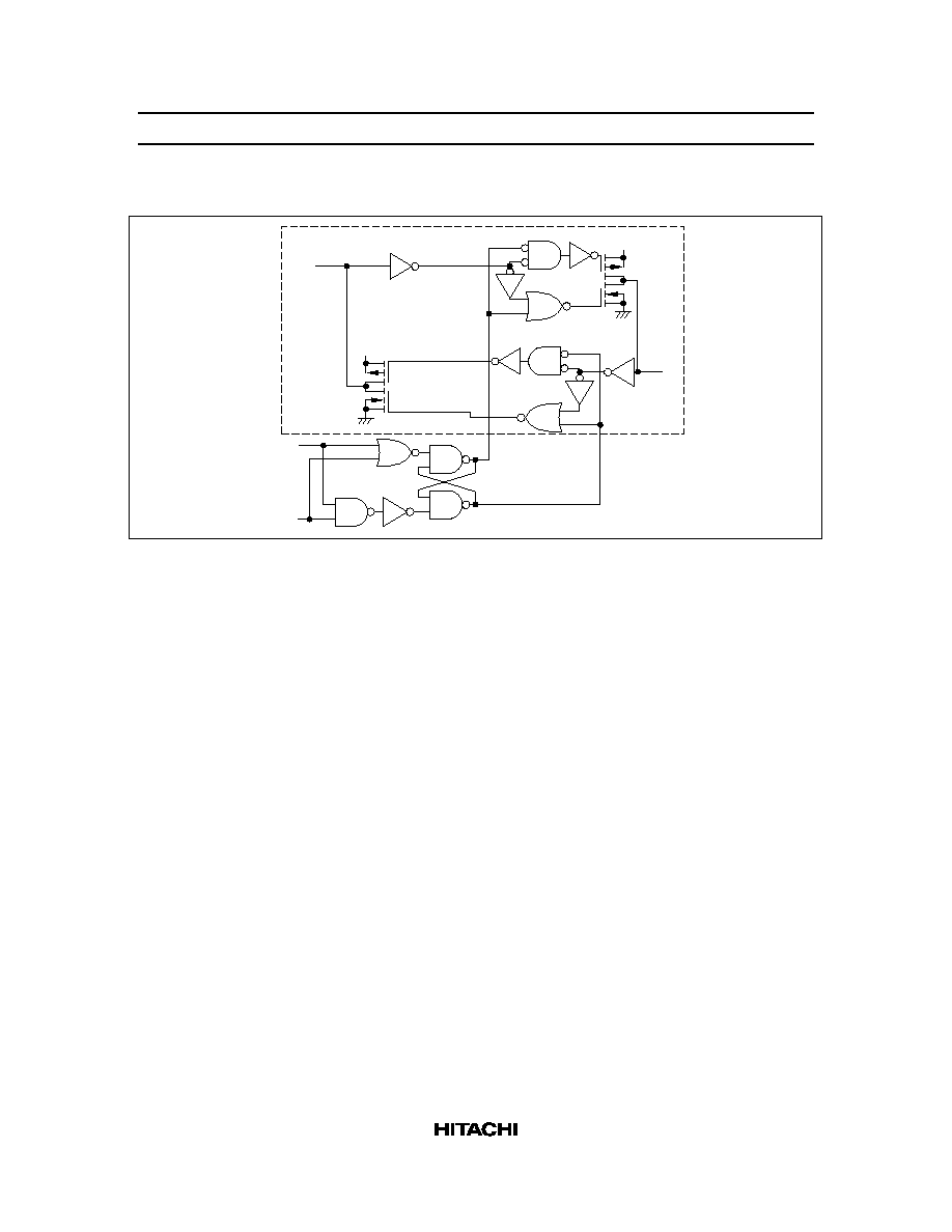
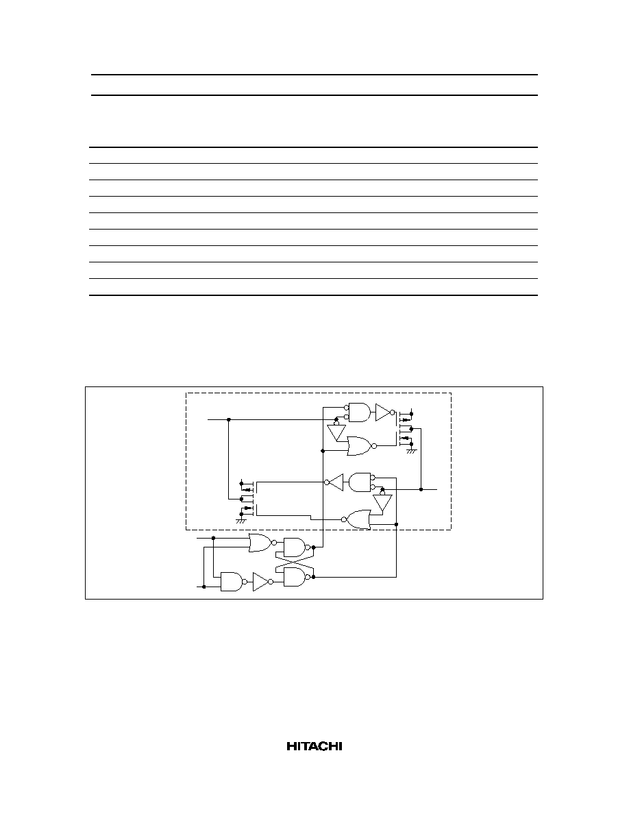
Logic Diagram
HD74HC242
GBA
A
B
V
CC
1 of 4
Transceivers
V
CC
G
AB