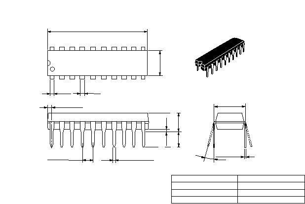
HD74HC377
Octal D-type Flip-Flops (with Enable)
Description
Information at the D inputs meeting the setup time requirements is transferred to the Q outputs on the
positive-going edge of the clock pulse if the enable input
G is low. Clock triggering occurs at a particular
voltage level and is not directly related to the transition time of the positive-going pulse. When the clock
input is at either the high or low level, the D input signal has no effect at the output. The circuits are
designed to prevent false clocking by transitions at the
G input.
Features
∑
High Speed Operation: t
pd
= 13 ns typ (C
L
= 50 pF)
∑
High Output Current: Fanout of 10 LSTTL Loads
∑
Wide Operating Voltage: V
CC
= 2 to 6 V
∑
Low Input Current: 1 µA max
∑
Low Quiescent Supply Current: I
CC
(static) = 4 µA max (Ta = 25∞C)
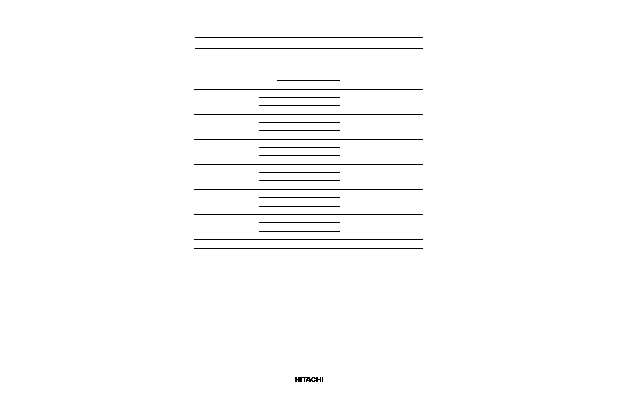
Function Table
Inputs
Outputs
Enable
G
Clock
Data
Q
Q
H
X
X
Q
0
Q
0
L
H
H
L
L
L
L
H
X
L
X
Q
0
Q
0